Axell Wireless 50-0253SERIES UHF Signal Extender User Manual RECEIVER MULTICOUPLER
Axell Wireless UHF Signal Extender RECEIVER MULTICOUPLER
UserManual.wiki
>
Axell Wireless
>
50 0253SERIES User Manual
manual
Navigation menu
Upload a User Manual
Namespaces
Wiki Guide
HTML
PDF
Info
Views
User Manual
Discussion / Help
Navigation
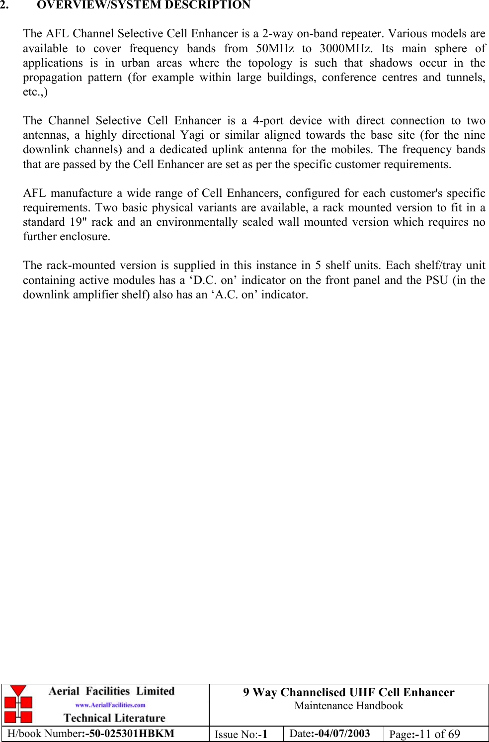
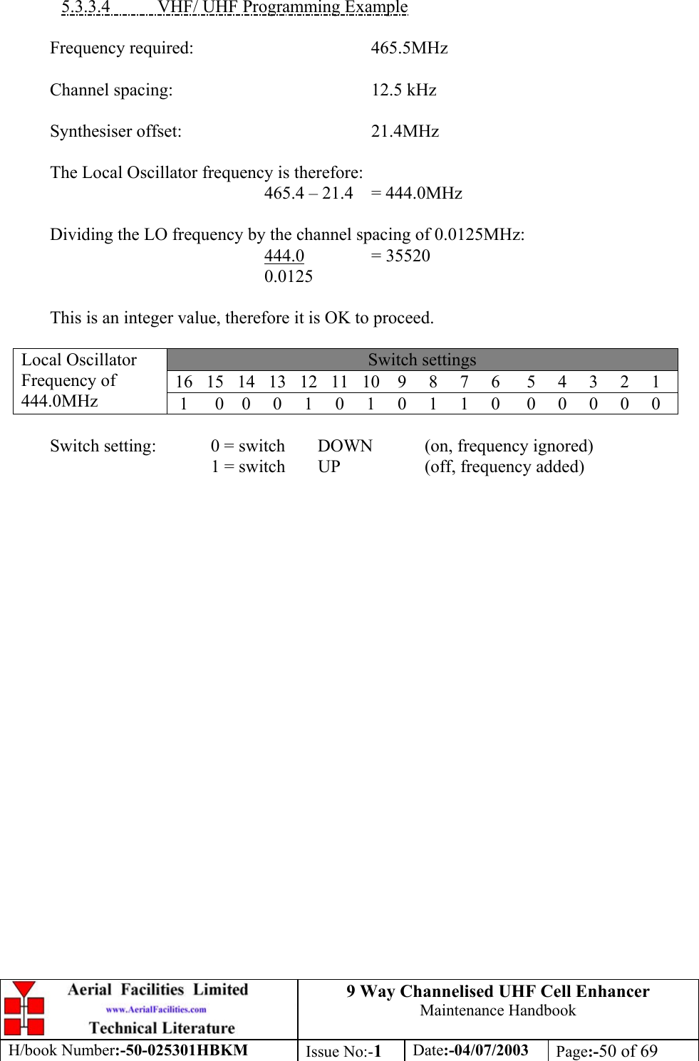
![9 Way Channelised UHF Cell EnhancerMaintenance HandbookH/book Number:-50-025301HBKM Issue No:-1Date:-04/07/2003 Page:-13 of 693.1.2 VTA Downlink Amplifier Shelf 50-025303 Parts ListAFL Part N.Description Qty.05-002603 UHF 3dB SPLITTER SMA 210-000701 1/4W0-30dB SWITCHED ATTENUATOR 211-006102 LNA 380-500MHz 1W WITH RELAY 211-007302 LNA. 380-500MHz 20dB (C/W RELAY) GA 111-007402 LNA. 380-500MHz 30dB (C/W RELAY) GA 312-002201 3 STAGE AMPLIFIER ALARM BOARD 212-002220 3 STAGE ALARM PCB COVER 212-004201 PWR AMP.450MHz 20W version CLASS A 213-001702 VOLTAGE REGULATOR Board 12V 250-012820 CCE RACK MOUNTED 8U CHASSIS 150-012822 CCE RACK MOUNTED LID 150-012825 CCE RACK MOUNTED HEATSINK BRACKET 450-027720 RACK MTD CHAN C.E. MODIFIED HEATSIN 280-008902 24V RELAY PCB ASSEMBLY 180-032320 10W PA HEATSINK (NEEDS 17-000526) 180-090822 C/E 8U FRONT PANEL, AFL (RAL7035) 191-030002 N ADAPTOR PANEL FEMALE:FEMALE 891-100003 SMA PLUG ELBOW UT-141 491-130001 SMA ADAPT 'T' ALL FEMALE 3 GHZ 191-520003 POWER SWITCHD/FUSED MAINS INL. 191-600014 'D' 9 WAY SOCKET S/B (NON FILTERED) 291-600015 'D' 9 WAY PLUG S/B (NON FILTERED) 191-700017 ICD 15 WAY 0.1' CONNECTOR 593-540035 1K3 0.25W 1% RES MRS25 M:F 296-300054 24V 17A PSU 400W (XP BCC) 196-500005 DC INPUT FILTERS 196-700002 LED.GREEN 5mm SEALED IP66 196-700005 LED.RED 5mm SEALED IP66 197-400002 HANDLE TYPE H6803 4U.[ALLOY] 2](https://usermanual.wiki/Axell-Wireless/50-0253SERIES/User-Guide-360817-Page-13.png)
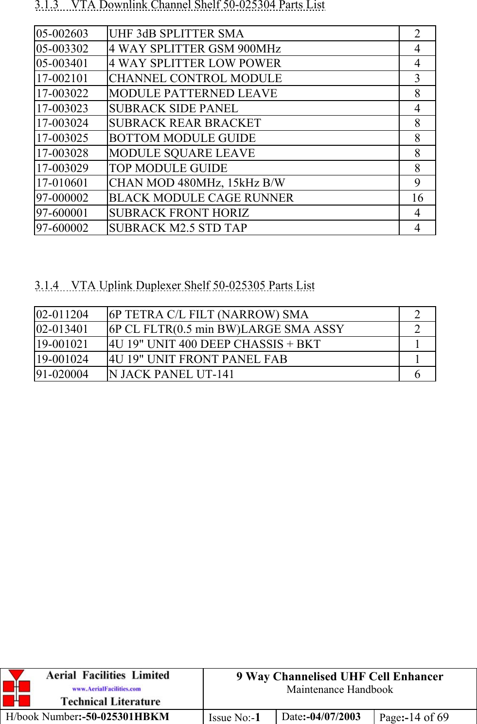
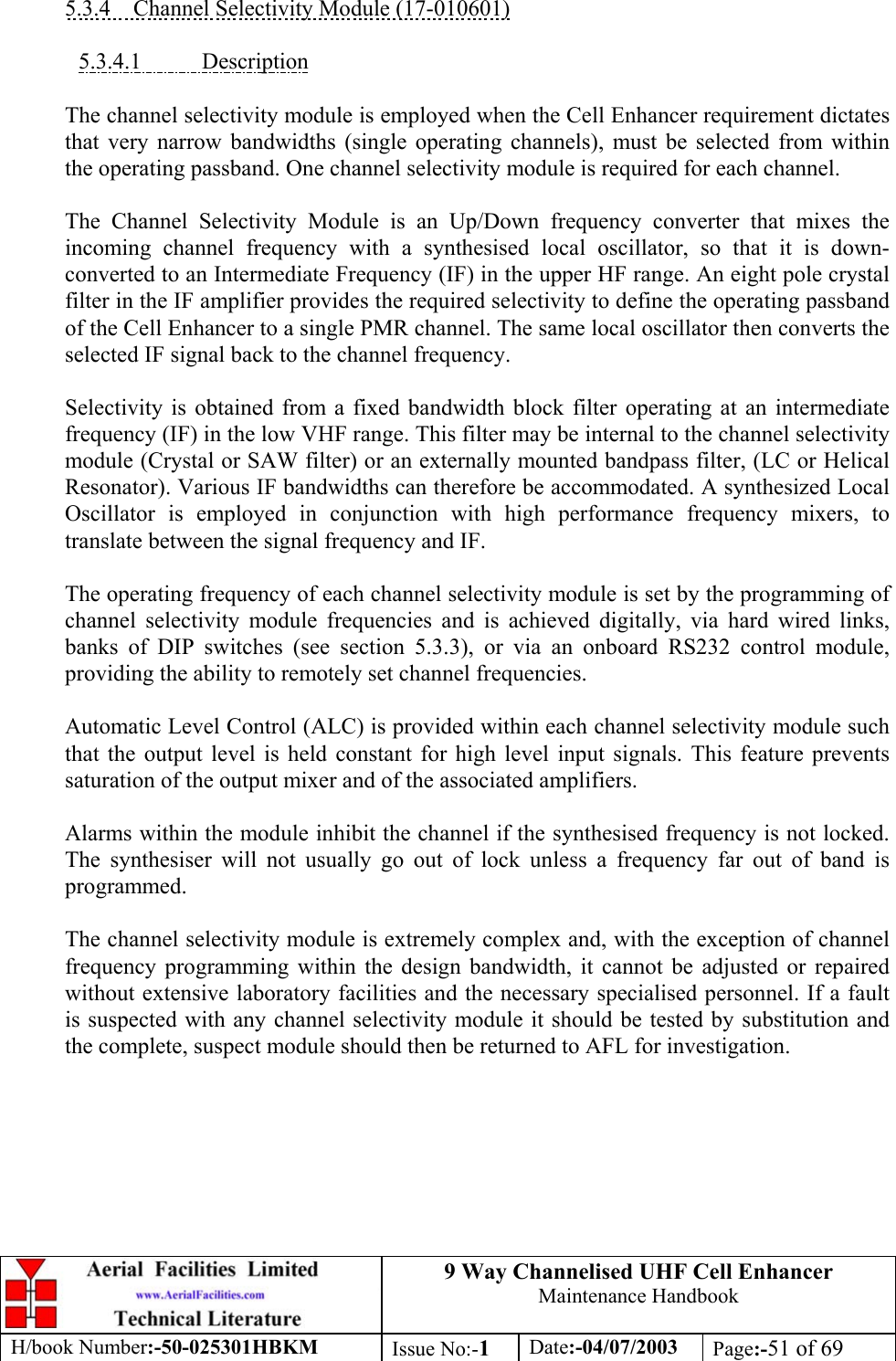
![9 Way Channelised UHF Cell EnhancerMaintenance HandbookH/book Number:-50-025301HBKM Issue No:-1Date:-04/07/2003 Page:-15 of 693.1.5 VTA Uplink Amplifier Shelf 50-025306 Parts List02-011204 6P TETRA C/L FILT (NARROW) SMA 102-013401 6P CL FLTR(0.5 min BW)LARGE SMA ASSY 110-000701 1/4W0-30dB SWITCHED ATTENUATOR 211-006102 LNA 380-500MHz 1W WITH RELAY 111-007302 LNA. 380-500MHz 20dB (C/W RELAY) GA 311-007402 LNA. 380-500MHz 30dB (C/W RELAY) GA 312-016301 PA 380-470MHz 20W CLASS A 113-001702 VOLTAGE REGULATOR Board 12V 213-003011 DC/DC CONVERTER 24-12V 8A PCB ASSY 117-001101 CELL ENHANCER AGC DETECTOR/AMP ASS 217-001201 C/E AGC UNIT ATTENUATOR ASSY 250-012820 CCE RACK MOUNTED 8U CHASSIS 150-012822 CCE RACK MOUNTED LID 150-012825 CCE RACK MOUNTED HEATSINK BRACKET 450-027720 RACK MTD CHAN C.E. MODIFIED HEATSIN 280-008902 24V RELAY PCB ASSEMBLY 180-032320 10W PA HEATSINK (NEEDS 17-000526) 180-090822 C/E 8U FRONT PANEL, AFL (RAL7035) 191-030002 N ADAPTOR PANEL FEMALE:FEMALE 491-100003 SMA PLUG ELBOW UT-141 491-130001 SMA ADAPT 'T' ALL FEMALE 3 GHZ 191-520003 POWER SWITCHD/FUSED MAINS INL. 191-600014 'D' 9 WAY SOCKET S/B (NON FILTERED) 291-600015 'D' 9 WAY PLUG S/B (NON FILTERED) 193-540035 1K3 0.25W 1% RES MRS25 M:F 296-300054 24V 17A PSU 400W (XP BCC) 196-500005 DC INPUT FILTERS 196-700002 LED.GREEN 5mm SEALED IP66 196-700005 LED.RED 5mm SEALED IP66 197-400002 HANDLE TYPE H6803 4U.[ALLOY] 2](https://usermanual.wiki/Axell-Wireless/50-0253SERIES/User-Guide-360817-Page-15.png)