Bird Technologies Group 5PI613805 SIGNAL BOOSTER User Manual 9408cvr 1 2
Bird Technologies Group SIGNAL BOOSTER 9408cvr 1 2
UserManual.wiki
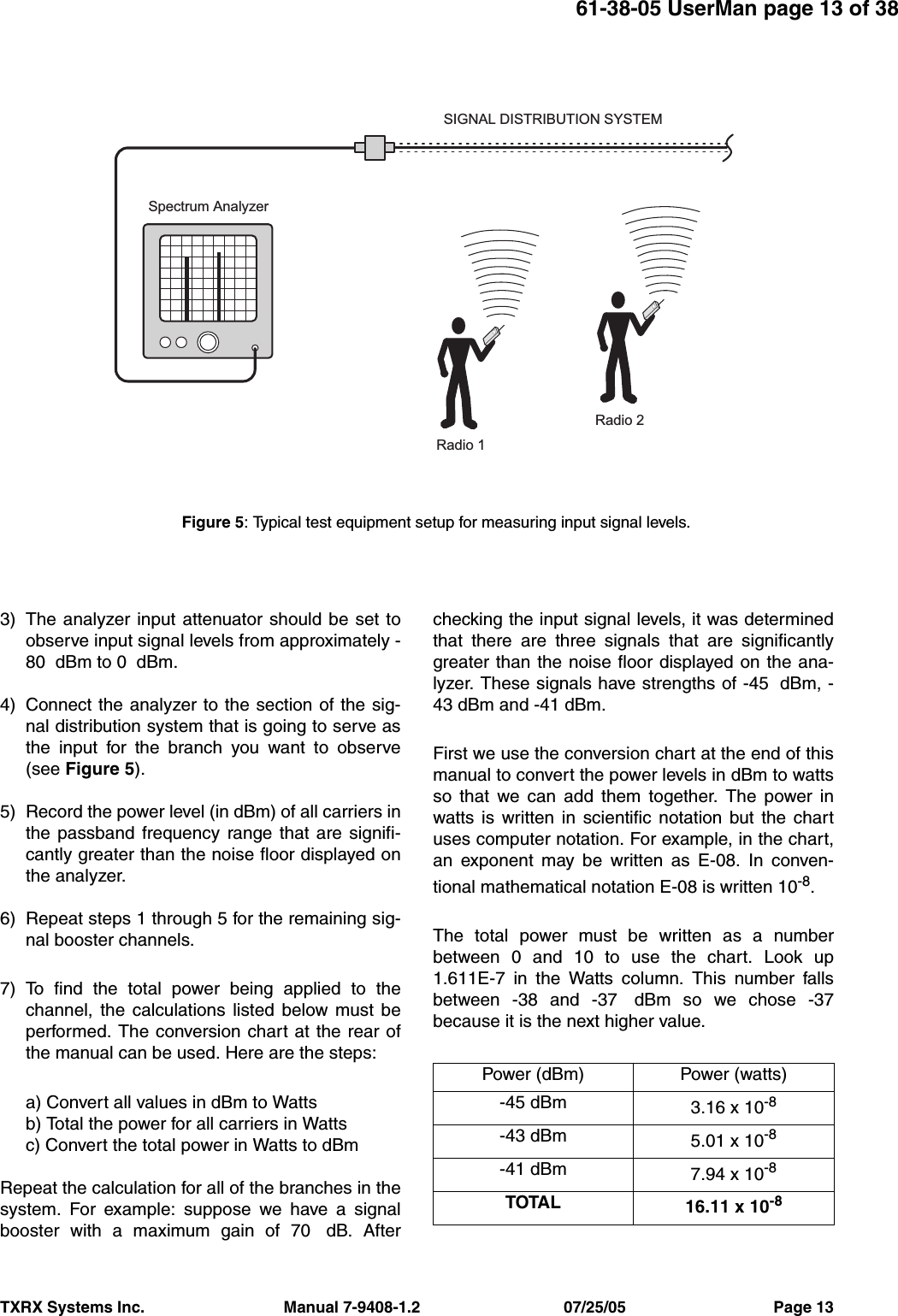
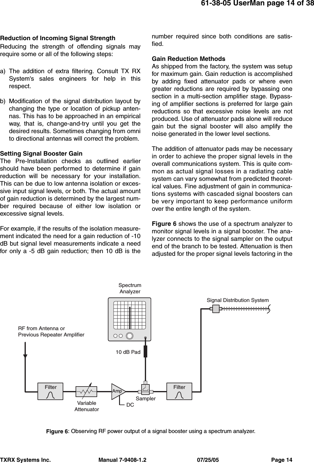
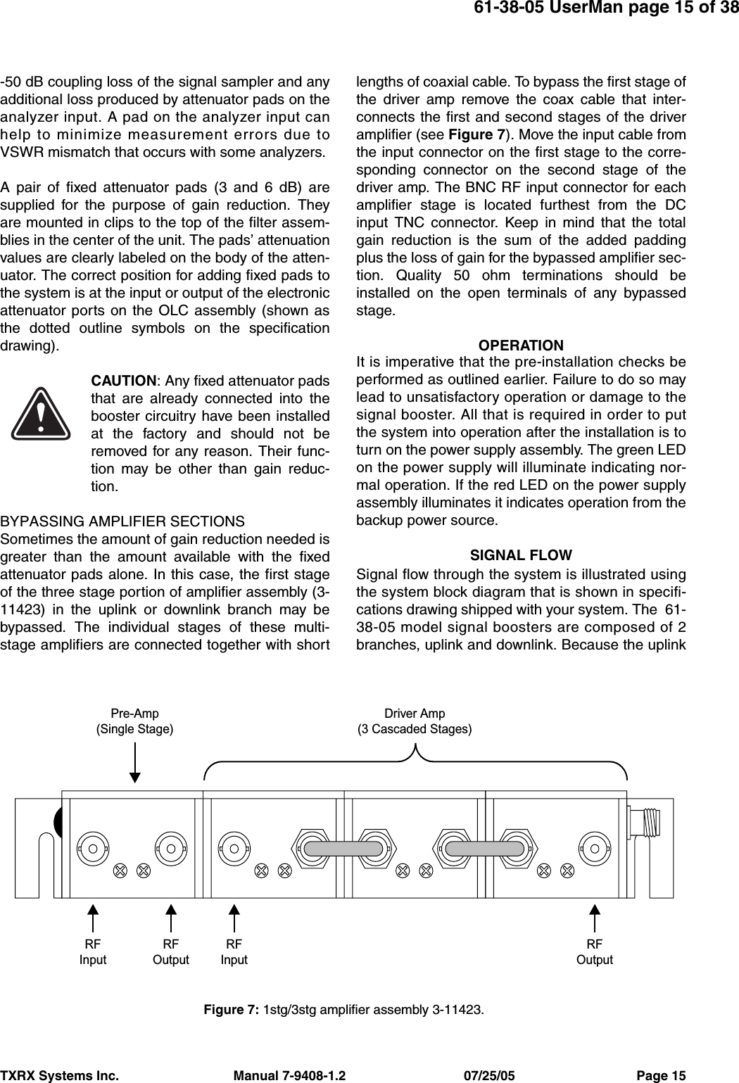
>
Bird Technologies Group
>
5PI613805 User Manual
USERS MANUAL
Navigation menu
Upload a User Manual
Namespaces
Wiki Guide
HTML
PDF
Info
Views
User Manual
Discussion / Help
Navigation