Bwave Technology TETHYS Tethys User Manual revised
Shanghai Bwave Technology Co.,Ltd. Tethys Users Manual revised
UserManual.wiki
>
Bwave Technology
>
TETHYS User Manual
>
Users Manual revised
Contents
1.
Users Manual
2.
Users Manual revised
Users Manual revised
Navigation menu
Upload a User Manual
Namespaces
Wiki Guide
HTML
PDF
Info
Views
User Manual
Discussion / Help
Navigation
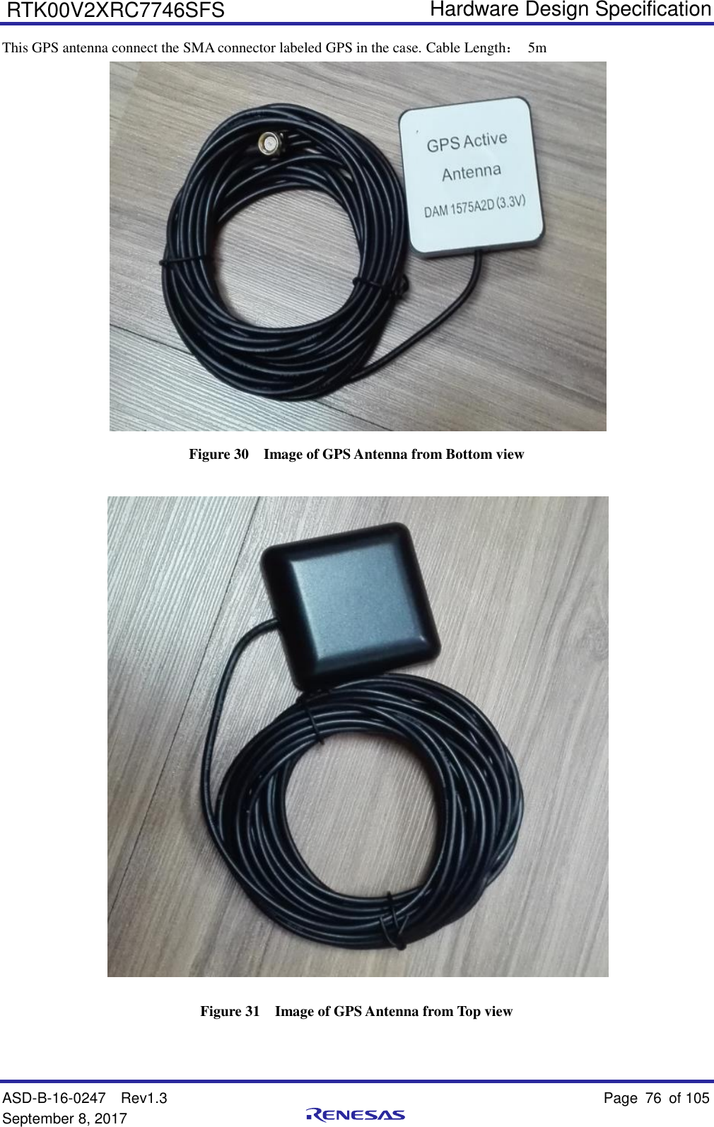
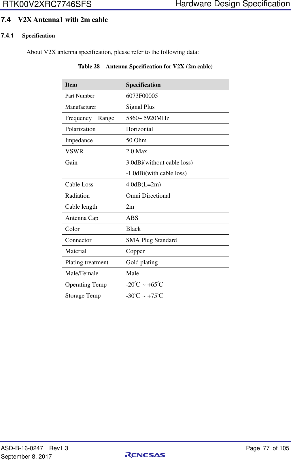
![Hardware Design Specification ASD-B-16-0247 Rev1.3 Page 2 of 105 September 8, 2017 RTK00V2XRC7746SFS CONTENTS 1 OVERVIEW ..........................................................................................................................................9 1.1 FEATURES ............................................................................................................................................ 10 1.1.1 Features of the Tethys Board ..................................................................................................... 10 1.1.2 Functions of the Tethys Board .................................................................................................... 11 1.2 USAGE NOTES ...................................................................................................................................... 12 1.2.1 Specifications of the Tethys Board ............................................................................................. 12 1.3 BOARD CONFIGURATION ....................................................................................................................... 13 1.3.1 Block Diagram of the Tethys Board ........................................................................................... 13 2 OPERATING CONDITION AND ANTENNA CHARACTERISTIC ....................................................... 14 2.1 OPERATING CONDITION ......................................................................................................................... 14 3 SPECIFICATIONS OF INTERFACE MODULES ON THE TETHYS BOARD ....................................... 15 3.1 MODE SETTING .................................................................................................................................... 15 3.1.1 Specifications ............................................................................................................................. 15 3.1.2 MD0 Pin -Selection of Free-Running Mode or Step-Up Mode .................................................. 15 3.1.3 MD [3:1] Pins-Selection of Boot Device ..................................................................................... 15 3.1.4 MD4 Pin-Selection of CS0 Space Size ...................................................................................... 15 3.1.5 MD5 Pin-Reserved ..................................................................................................................... 15 3.1.6 MD [7:6] Pins-Selection of Master Boot Processor ................................................................... 15 3.1.7 MD8 Pin-Selection of Area 0 Space Data Bus Width ................................................................ 16 3.1.8 MD9 Pin-Selection of Crystal Resonator or Crystal Oscillator ................................................... 16 3.1.9 MD21, MD20, MD11, MD10, and MDT [1:0] Pins-Switching of JTAG, SDHI1, and SDHI2 ....... 16 3.1.10 MD [14:13] Pins-Frequency Mode Setting ................................................................................. 17 3.1.11 Initial Values of Mode Setting Pins on Tethys Board ................................................................. 17 3.2 DDR3-SDRAM INTERFACE (DBSC) ...................................................................................................... 17 3.2.1 Specifications ............................................................................................................................. 17 3.2.2 Signal Connections between R-Car W2H and DDR3-SDRAMs ................................................ 18 3.2.3 Block Diagram ............................................................................................................................ 19 3.3 SPI-FLASH INTERFACE (QSPI) ............................................................................................................... 20 3.3.1 Specifications ............................................................................................................................. 20 3.3.2 Block Diagram ............................................................................................................................ 20 3.4 AUDIO CODEC INTERFACES (SSI0, SSI1) ................................................................................................ 21 3.4.1 Specifications ............................................................................................................................. 21 3.4.2 Block Diagram ............................................................................................................................ 21 3.5 EMMC MEMORY INTERFACE (EMMC) ................................................................................................... 22 3.5.1 Specifications ............................................................................................................................. 22](https://usermanual.wiki/Bwave-Technology/TETHYS.Users-Manual-revised/User-Guide-3665297-Page-2.png)
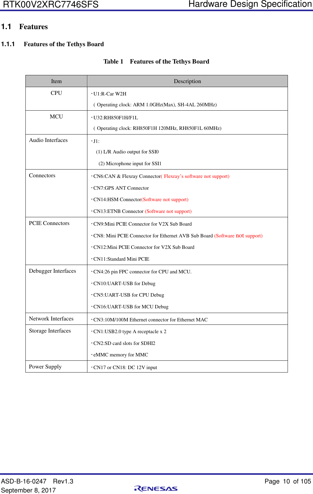
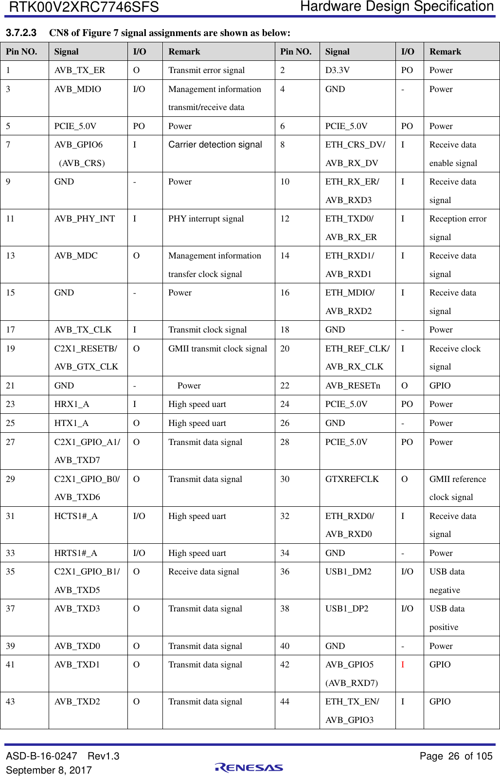
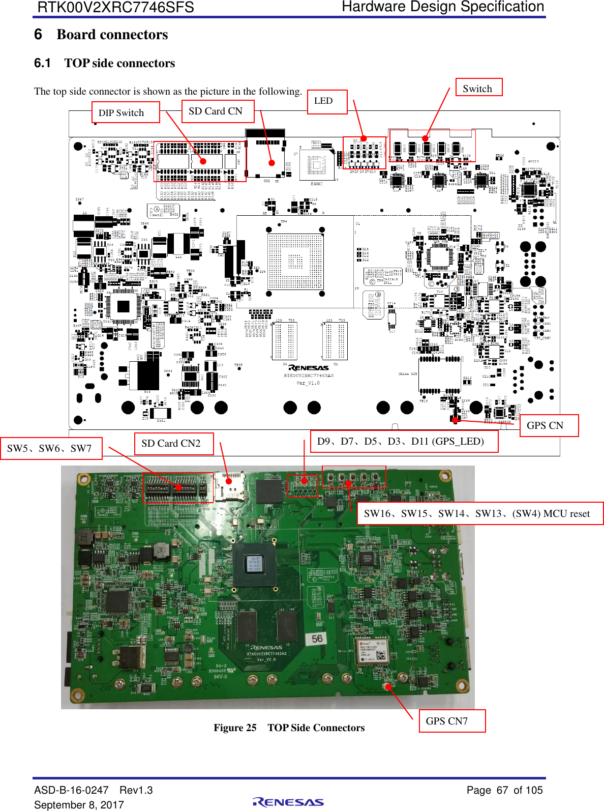
![Hardware Design Specification ASD-B-16-0247 Rev1.3 Page 11 of 105 September 8, 2017 RTK00V2XRC7746SFS 1.1.2 Functions of the Tethys Board Table 2 List of Tethys Board Functions Board Function Tethys RAM DDR3 I/F: DDR3-SDRAM 1600MHz 1 GB x2 USB 2.0 USB2.0 CH0 : USB2.0 type A USB2.0 CH1 : USB2.0 type A SDHI SDHI0 : Mini PCIE Connector for V2X Sub Board SDHI2 : SD card slots , Mini PCIE Connector for V2X Sub Board SCIF SCIF0_D/HSCIF0_B : (1) Mini PCIE Connector for V2X Sub Board , (2) UART-USB SCIF3_B/HSCIF2 : Mini PCIE Connector for V2X Sub Board SCIF2_B(Debug serial) : UART-USB for CPU Debug SCIF5_C : GPS Module ROM(QSPI) QSPI0 : SPI Flash 64MB QSPI1 : SPI Flash 4MB Ethernet MAC / Ethernet AVB Ethernet MAC: RJ45 Connector Ethernet AVB: Mini PCIE Connector for Ethernet AVB Sub Board (Ethernet AVB’s software not support) HSCIF HSCIF1_A: Mini PCIE Connector for Ethernet AVB Sub Board (Ethernet AVB’s software not support) SCIF0_D/HSCIF0_B : (1) Mini PCIE Connector for V2X Sub Board , (2) UART-USB SCIF3_B/HSCIF2 : Mini PCIE Connector for V2X Sub Board I2C I2C1_A/SPI : HSM Connector (Software not support) I2C1_A : G-Sensor , Gyro , MCU SSI SSI0,1,2,9 : Audio CODEC MSIOF MSIOF1_B : MCU [Flexray (Software not support)、Ethernet AVB’s software not support] MMC MMC : eMMC(8GB) PCI Express Mini PCIE Connector CAN R-CAR W2H CAN channel support, RH850 CAN0/1 support, Flexray Software not support Debug I/F DBG : TO Sub Connector VCC Power Block .](https://usermanual.wiki/Bwave-Technology/TETHYS.Users-Manual-revised/User-Guide-3665297-Page-11.png)
![Hardware Design Specification ASD-B-16-0247 Rev1.3 Page 15 of 105 September 8, 2017 RTK00V2XRC7746SFS 3 Specifications of Interface Modules on the Tethys Board This section describes the main function of the Tethys board, which includes the following sections: 3.1 Mode Setting 3.1.1 Specifications The operating mode of the R-Car W2HR-Car W2H is set by a power-on reset. For details on the operating mode, see the documents related to the R-Car W2HR-Car W2H operating mode specifications. 3.1.2 MD0 Pin -Selection of Free-Running Mode or Step-Up Mode Do not change the initial setting at shipment (MD0=0). 3.1.3 MD [3:1] Pins-Selection of Boot Device These pins select the boot device. MD3 MD2 MD1 Selection of Boot Device 0 0 0 External ROM boot (area 0) 0 0 1 eMMC boot via SDHI1 0 1 0 Serial flash ROM boot via QSPI; 16Kbytes transferred at 48.75 MHz 0 1 1 Reserved 1 0 0 Serial flash ROM boot via QSPI; 16Kbytes transferred at 39 MHz 1 0 1 Reserved 1 1 0 Serial flash ROM boot via QSPI; 4 Kbytes transferred at 39 MHz 1 1 1 Reserved 3.1.4 MD4 Pin-Selection of CS0 Space Size This pin selects whether the area 0 space (CS0) is used as a normal space (64 Mbytes) or an expanded space (128 Mbytes). MD4 Area Division 0 Area 0: 64 Mbytes 1 Area 0: 128 Mbytes 3.1.5 MD5 Pin-Reserved Do not change the initial setting at shipment (MD5=1). 3.1.6 MD [7:6] Pins-Selection of Master Boot Processor These pins select the master boot processor.](https://usermanual.wiki/Bwave-Technology/TETHYS.Users-Manual-revised/User-Guide-3665297-Page-15.png)
![Hardware Design Specification ASD-B-16-0247 Rev1.3 Page 16 of 105 September 8, 2017 RTK00V2XRC7746SFS MD7 MD6 Selection of Master Boot Processor 0 0 Setting prohibited 0 1 Booted through CPU0 in CA7. 1 0 Booted through SH-4AL in 32-bit mode 1 1 Setting prohibited 3.1.7 MD8 Pin-Selection of Area 0 Space Data Bus Width This pin sets the data bus width of the area 0 space (CS0) to 8 bits or 16 bits. Select the data bus width of the boot device connected to the LBSC. MD8 EXBUS Area 0 Data Bus Width 0 8-bit bus 1 16-bit bus 3.1.8 MD9 Pin-Selection of Crystal Resonator or Crystal Oscillator This pin selects either a crystal resonator or a crystal oscillator to be connected to the EXTAL/XTAL pins. A crystal oscillator (Y2: 20 MHz) is mounted on the Tethys board by default. MD9 EXTAL/XTAL Pin Setting 0 An external clock is input to the EXTAL pin. 1 A crystal resonator is connected to the EXTAL and XTAL pins. 3.1.9 MD21, MD20, MD11, MD10, and MDT [1:0] Pins-Switching of JTAG, SDHI1, and SDHI2 These pins select the debugging function through the JTAG connector (CN4) or the SD card slot for the SDHI1. The debugging through the SDHI1 or SDHI2 is possible by the combination of MD pin settings in the R-Car W2H specifications. MD10 MD[21:20] MD11 MDT[1:0] JTAG MMC SDHI2 0 00 - -- Boundary scan Normal function Normal function 0 01 - -- Reserved Reserved Reserved 0 10 0 -- Coresight (*1) Normal function Normal function 0 10 1 00 Coresight (*1) Reserved Reserved 0 10 1 01 Coresight (*1) SH-4AL Normal function 0 10 1 10 Coresight (*1) Reserved Reserved 0 10 1 11 Coresight (*1) Normal function SH-4AL 0 11 0 -- SH-4AL Normal function Normal function 0 11 1 00 SH-4AL Coresight (*1) Normal function 1 00 - -- Reserved Reserved Reserved 1 01 0 -- Reserved Reserved Reserved 1 01 1 01 Reserved Reserved Reserved 1 10 - -- Reserved Reserved Reserved 1 11 - -- Reserved Reserved Reserved](https://usermanual.wiki/Bwave-Technology/TETHYS.Users-Manual-revised/User-Guide-3665297-Page-16.png)
![Hardware Design Specification ASD-B-16-0247 Rev1.3 Page 17 of 105 September 8, 2017 RTK00V2XRC7746SFS (*1) “Coresight” is an abbreviation of “Coresight debug port”. 3.1.10 MD [14:13] Pins-Frequency Mode Setting These pins select the frequency mode. A crystal oscillator (Y2: 20 MHz) is mounted on the Tethys board. Do not change the initial setting at shipment (MD14 = 0, MD13 = 0). MD14 MD13 EXTAL Frequency EXTAL Divider PLL0 Multiplication Ratio PLL1 Multiplication Ratio PLL3 Multiplication Ratio 0 0 20 MHz × 1 ×80 VCO = 1600 MHz ×78 VCO = 1560 MHz ×50 VCO = 1000 MHz 0 1 26 MHz × 1 ×60 VCO = 1560 MHz ×60 VCO = 1560 MHz ×56 VCO = 1456 MHz 1 0 Prohibited setting 1 1 30 MHz × 1 ×52 VCO = 1560 MHz ×52 VCO = 1560 MHz ×50 VCO = 1500 MHz 3.1.11 Initial Values of Mode Setting Pins on Tethys Board The following table shows the Initial Values of Mode Setting Pins on the Board, and how the individual mode pins are set: MD Pins Initial Value Initial Function Setting Method MD0 0 - Set by a dip switch MD[3:1] 010 Boot from the QSPI(48.75 MHz/16-Kbyte transfer) Set by a dip switch MD4 0 CS0 space size (64 Mbytes) Set by a dip switch MD5 1 - Set by a dip switch MD[7:6] 01 Cortex-A7 boot Set by a dip switch MD8 1 CS0 space data bus width (16 bits) Set by a dip switch MD9 1 Crystal resonator is used. Set by a dip switch MD10, MD[21:20], MD11, MDT[1:0] 0,10,0,00 JTAG = Coresight SDHI1 and SDHI2 = Normal function Set by a dip switch MD[14:13] 00 Input frequency = 20 MHz Set by a dip switch 3.2 DDR3-SDRAM Interface (DBSC) 3.2.1 Specifications The Tethys board incorporates two 4-Gbit DDR3-SDRAMs (16-bit bus width) and operates at a maximum speed of](https://usermanual.wiki/Bwave-Technology/TETHYS.Users-Manual-revised/User-Guide-3665297-Page-17.png)
![Hardware Design Specification ASD-B-16-0247 Rev1.3 Page 18 of 105 September 8, 2017 RTK00V2XRC7746SFS DDR3-1000. The Tethys board can support memory size up to 2GB (8-Gbit memory x 2) and the data bus width is 32 bits x1. The DDR3-SDRAMs are allocated to the address space from H'01_0000 0000 to H'01_FFFF FFFF in the R-Car W2H. The address ranges from H'00_40000000 to H'00_BFFF FFFF can be accessed by default as a mirror area of H'01_0000 0000 to H'01_7FFF FFFF. Table 4 DDR3-SDRAM Interface Specifications Controller On-chip external bus controller for DDR3-SDRAM (DBSC) in the R-Car W2H Product name MT41K256M16HA-125 AAT:E from Micron DDR3-1600 (x 16 bits, 4 Gbits) x 2 pcs Power supply voltage 1.50 V Capacity H'01_0000 0000 to H'01_FFFF FFFF Bus width 32-bit data bus Memory bus frequency(R-Car W2H Spec.) DDR3-1000 3.2.2 Signal Connections between R-Car W2H and DDR3-SDRAMs Table 5 Signal Connections between R-Car W2H and DDR3-SDRAMs R-Car W2H DDR3-SDRAM (U3) DDR3-SDRAM (U4) D[31:16] D[15:0] M0DQ[31:16] DQ[15:0] -- M0DQ[15:0] -- DQ[15:0] M0A[15:0] A[15:0] ← M0BA[2:0] BA[2:0] ← M0CK1、M0CK1# CK、CK# -- M0CK0、M0CK0# -- CK、CK# MCKE1 CKE -- MCKE0 -- CKE M0CS1# CS# -- M0CS0# -- CS# M0WE# WE# ← M0RAS# RAS#A ← M0CAS# CAS# ← M0DQS3、M0DQS3# UDQS、UDQS# -- M0DQS2、M0DQS2# LDQS、LDQS# -- M0DQS1、M0DQS1# -- UDQS、UDQS# M0DQS0、M0DQS0# -- LDQS、LDQS# M0DM3、M0DM2 UDM、LDM -- M0DM1、M0DM0 -- UDM、LDM](https://usermanual.wiki/Bwave-Technology/TETHYS.Users-Manual-revised/User-Guide-3665297-Page-18.png)
![Hardware Design Specification ASD-B-16-0247 Rev1.3 Page 19 of 105 September 8, 2017 RTK00V2XRC7746SFS M0ODT1 ODT -- M0ODT0 -- ODT M0RESET# RESET# ← 3.2.3 Block Diagram R-CarW2HM0DQ[31:0]M0A[15:0]M0BA[2:0]M0RAS#M0CAS#M0WE#M0RESET#M0CS0#M0CKE0M0ODT0M0CK0M0CK0#M0DQS[1:0]M0DQS[1:0]#M0DM[1:0]M0CKE1M0ODT1M0CK1M0CK1#M0DQS[3:2]M0DQS[3:2]#M0DM[3:2]M0BKPRST#M0VREFDQ1M0VREFDQ0M0VREFCAM0ZQA[15:0]BA[2:0]RAS#CAS#WE#RESET#CS#CKEODTCKCK#DQSDQS#DMDQSDQS#DMDQL[7:0]DQU[7:0]VREFCAVREFDQDQL[7:0]DQU[7:0]0.1uF 0.1uF0.1uF20K20KDDR30.1uF 0.1uF0.1uF20K20KM0BKPRST D1.5V D1.5V120MT41K256M16HA-125 AAT:E0.1uF 0.1uF20K20K2222222222M0CS1# CS#2222CKE222222100M0ZQ240ODTCKCK#D1.5V0.1uF515100.1uF Figure 2 Block Diagram of the DDR3-SDRAM Interface](https://usermanual.wiki/Bwave-Technology/TETHYS.Users-Manual-revised/User-Guide-3665297-Page-19.png)
![Hardware Design Specification ASD-B-16-0247 Rev1.3 Page 22 of 105 September 8, 2017 RTK00V2XRC7746SFS 3.5 eMMC Memory Interface (eMMC) 3.5.1 Specifications The Tethys board incorporates an eMMC memory SDIN8DE1-8G-XA manufactured by SanDisk that is connected to the on-chip MMC interface of the R-Car W2H.For details on the MMC, see the R-Car W2H Hardware Manual. Table 8 eMMC Memory Interface (eMMC) Specifications MMC controller On-chip MMC in the R-Car W2H Interface voltage control D3.3V_eMMC=3.3V eMMC memory SDIN8DE1-8G-XA(U7) from SanDisk Capacity:8GB 3.5.2 Block Diagram MMC_CLKMMC_CMDMMC_D[7:0]VCCQ_MMCeMMCCLKCMDDATA[7:0]D3.3VVCCQVCCD3.3V_eMMC10KD3.3V_eMMCR-Car W2H Figure 5 Block Diagram of the eMMC Memory Interface](https://usermanual.wiki/Bwave-Technology/TETHYS.Users-Manual-revised/User-Guide-3665297-Page-22.png)
![Hardware Design Specification ASD-B-16-0247 Rev1.3 Page 23 of 105 September 8, 2017 RTK00V2XRC7746SFS 3.6 SD Card Host Interface (SDHI2) 3.6.1 Specifications The Tethys board incorporates a SD card slot (CN2) and a mini-PCI Express CN (CN12) for the on-chip SD card host interface (SDHI2) of the R-Car W2H. For details on the SDHI2, please refer to the R-Car W2H hardware manual. CN12 and CN2 can not be used at the same time. Table 9 Specifications of SD Card Host Interface (SDHI2) SD Host Interface On-chip SDHI2 in the R-Car W2H Voltage control for VDD VCCQ_SD2 =3.3V/1.8V it can be switched by software , D3.3V=3.3V SD Card Slot 503182-1852(CN2) from Molex 3.6.2 Block Diagram R-Car W2H SDHI2SD2_CLKSD2_DATA[3:0]SD2_CDSD2_WPSD2_CMDVCCQ_SD247K10033333333CLKDATA[3:0]WPCDCMDSD SlotCN2D3.3VD3.3V Figure 6 Block Diagram of the SDHI2 Interface](https://usermanual.wiki/Bwave-Technology/TETHYS.Users-Manual-revised/User-Guide-3665297-Page-23.png)
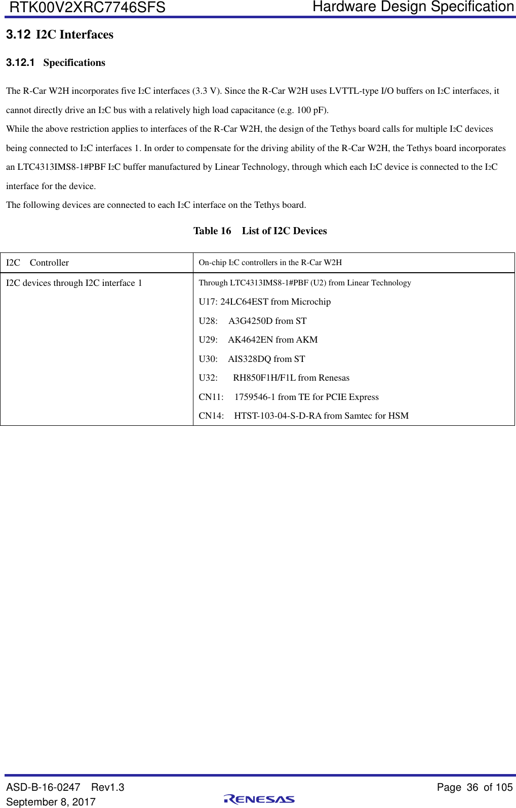
![Hardware Design Specification ASD-B-16-0247 Rev1.3 Page 37 of 105 September 8, 2017 RTK00V2XRC7746SFS 3.12.2 List of Slave Addresses The table below lists the slave addresses of the I2C devices on the Tethys board Table 17 List of I2C Slave Addresses I2C Interfaces Ux/CNx Device Slave Addresses Note Binary Hexadecimal SA7 SA6 SA5 SA4 SA3 SA2 SA1 R/W# RD WR 1 U17 24LC64EST I2C EEPROM for MAC address 1 0 1 0 0 0 0 x 0xA1 0xA0 *1 U28 A3G4250D GYRO 1 1 0 1 0 1 1 x 0xD7 0xD6 *2 U29 AK4642EN AUDIO 0 0 1 0 0 1 0 x 0x25 0x24 *3 U30 AIS328DQ G-SENSOR 0 0 1 1 0 0 1 x 0x33 0x32 *4 U32 RH850F1H/F1L MCU -- -- -- -- -- -- -- -- -- -- *5 CN11 Mini PCIE Connector -- -- -- -- -- -- -- -- -- -- CN14 HSM CN Connector -- -- -- -- -- -- -- -- -- -- - Note: *1 Pins 3 to 1 (A [2:0]) = GND *2 Pin 8 to 12 (RESERVED [5:1]) = GND *3 Pin 8 (CSN/CAD0) = GND *4 Pin 25(EP) and Pin 4 (RESERVED1) = GND *5 I2C no use 3.12.3 Block Diagram U2LTC4313IMS8-1#PBFU1R-Car W2HSCL1_ASDA1_ASCL SDAU1724LC64ESTSCL SDAU28A3G4250DU29AK4642ENSCL SDAU30AIS328DQSCL SDAU32RH850F1H/F1LSCL SDACN14HSM CNSCL SDACN11Mini PCIESCL SDA0033 332K 1% 2K 1% 2K 1% 2K 1%D3.3V D3.3V Figure 14 Block Diagram of the I2C Interfaces](https://usermanual.wiki/Bwave-Technology/TETHYS.Users-Manual-revised/User-Guide-3665297-Page-37.png)
![Hardware Design Specification ASD-B-16-0247 Rev1.3 Page 51 of 105 September 8, 2017 RTK00V2XRC7746SFS SI3433CDV-T1-E3(U13) BU3.3V BU3.3V_MCU supported (1*) CN17 and CN18 are 12V power connectors, use can choose one connector according to the demand 3.20.2 Block Diagram R2A11301FTMOS FETHAT2210RMOS FETHAT2210RGate Ctrl Gate CtrlBU12VFBFBVSYSFBBU12VRP111N331D-TR-AEBU5.0VMOSFET(Power Switch)Si3433CDV-T1-E3BU3.3V Flexray transceiver(max:350mA)MCUFlexray transceiver (max:350mA)MCU CAN (max:75mA)MCU CAN (max:75mA)MOSFET(Power Switch)Si3433CDV-T1-E3CPU CAN transceiver(max:75mA)To USB Host Type A Receptacle(max:500mA)To USB Host Type A Receptacle(max:500mA)To USB HUB: GL852GT-MNGXX(max:100mA)RP111N251D-TR-AEP3.3V D2.5V Main CPU(max:400mA)MOSFET(Power Switch)Si3433CDV-T1-E3P3.3V[LED (max:10mA)]X10SC183CULTRTTPS54531DDALM3102MHMain CPU(max:120mA)Micro SD slot(max:100mA)D1.2V Main CPU(max:3525mA)D1.5VMain CPU(max:450mA)DDR3(max:360mA)DDR3(max:360mA)PCIE CN(max:375mA)Main CPU(max:324mA)SPI Flash(max:100mA)SPI Flash(max:100mA)GPS Receive(Max:63mA)RMII PHY(min:53mA)EMMC(max:300mA)GYRO(max:7mA)G-SENSOR(max:450uA)AUDIO Codec(max:167mA)Micro SD slot(max:100mA)PCIE CN(max:1000mA)D3.3VTPS54531DDA [PCIE CN(max:1500mA)]X3P5.0VD5.0VD1.8VPCIE_5.0VBU12VCN18HEC0470-01-630(MJ-179P)CN1734793-9040SW18 132SW18:2-3 short: ON 1-2 short: OFFACC_CONT_EXTACC_CONT_EXTBU12VEN1/EN2MCU reset (max:0.005mA)CPU and MCU JTAG HSM CN Figure 22 Block Diagram of the Power System](https://usermanual.wiki/Bwave-Technology/TETHYS.Users-Manual-revised/User-Guide-3665297-Page-51.png)
![Hardware Design Specification ASD-B-16-0247 Rev1.3 Page 58 of 105 September 8, 2017 RTK00V2XRC7746SFS 4.2.2 Realize the UART with the baud rate of 115200 This UART uses RLIN31 of RH850’s LIN/UART interface. Edge detection circuitRLIN3nTXRLIN3nRXLINn registersLINn interruptcontroller circuitLINn baud rate generatorProtocol controllerLIN communication clock sourceINTRLIN3nUR0INTRLIN3nUR1INTRLIN3nUR2INTRLIN3nINTP1nRLIN3n Figure shows LIN/UART interface (in UART mode) transmission operations as follows Start bit(1)(2)(3) (4) (5)(6)(7)Idle Idle7 , 8, or 9 data bits0 or 1 parity bit1 or 2 stop bitsUART frameRLIN3nTX Figure shows the LIN/UART interface (in UART mode) reception operation as follows. (1)(2)(3)(4) (5)(6)(7)Idle Idle7 , 8, or 9 data bits0 or 1 parity bit1 or 2 stop bitsUART frameRLIN3nTX (about [NSPB], [IBS]’s definition, please refer to [r01uh0445ej0100_rh850f1h.pdf] page 937,859’s description). This UART’s operations are as follows: 1. 15: The NSPB bits select the number of sampling in one Tbit (reciprocal of the bit rate). 2. Noise filter ON: The noise filter is enabled when receiving data 3. Non-parity, 8bit, 1stop. 4. No space: The IBS bits set the width of the space between the UART frame in UART buffer transmit](https://usermanual.wiki/Bwave-Technology/TETHYS.Users-Manual-revised/User-Guide-3665297-Page-58.png)
![Hardware Design Specification ASD-B-16-0247 Rev1.3 Page 96 of 105 September 8, 2017 RTK00V2XRC7746SFS 7.9 Sub board Tortuga wireless module board dimension The Tethys board can connect to Tortuga wireless module through MINI PCIE interface transfer board, and the transfer sub board dimension is shown as below(Unit: mm): Please connect this board to CN9, CN12. 7.9.1 RF characteristic *1 typical operating condition (Just informative, not guaranteed.): *1 HW = Tortuga7, Ta = 25°C, VDD3V3 =3.3V, VDD1V2 =1.2V, VDD5V0=5.0V *1 Measurement point is circled in red in the figure below (1) Receive characteristic Min Typ Max Unit Condition Frequency range 5850 5925 [MHz] Input VSWR 2.0 - 5890MHz Minimum Sensitivity (Diversity off) -94 [dBm] Data rate = 3Mbps -93 [dBm] Data rate = 6Mbps -87 [dBm] Data rate = 12Mbps -77 [dBm] Data rate = 27Mbps Minimum Sensitivity (Diversity on) -94 [dBm] Data rate = 3Mbps -94 [dBm] Data rate = 6Mbps -87 [dBm] Data rate = 12Mbps -80 [dBm] Data rate = 27Mbps Maximum Input Level (Diversity off) -20 [dBm] Data rate = 27Mbps Maximum Input Level (Diversity on) -20 [dBm] Data rate = 27Mbps Adjacent channel rejection (Diversity off) 30 [dB] Data rate = 3Mbps 29 [dB] Data rate = 6Mbps 28 [dB] Data rate = 12Mbps 18 [dB] Data rate = 27Mbps Nonadjacent Adjacent channel rejection (Diversity off) 44 [dB] Data rate = 3Mbps 41 [dB] Data rate = 6Mbps 36 [dB] Data rate = 12Mbps 27 [dB] Data rate = 27Mbps (2) Transmit characteristic](https://usermanual.wiki/Bwave-Technology/TETHYS.Users-Manual-revised/User-Guide-3665297-Page-96.png)
![Hardware Design Specification ASD-B-16-0247 Rev1.3 Page 97 of 105 September 8, 2017 RTK00V2XRC7746SFS Ta = 25°C, VDD3V3 =3.3V, VDD1V2 =1.2V, VDD5V0=5.0V Min Typ Max Unit Condition Frequency range 5850 5925 [MHz] Output VSWR 2.0 5890MHz Maximum out put Power(ANT_B) 24 [dBm] 5890MHz Maximum out put Power(ANT_A) -8 [dBm] 5890MHz Minimum out put Power(ANT_B) -7 [dBm] 5890MHz Minimum out put Power(ANT_A) -35 [dBm] 5890MHz Output Power control range 30 [dB] 5890MHz Power control step 0.5 [dB] Relative constellation error -28 [dB] Data rate = 3Mbps -28 Data rate = 6Mbps -28 Data rate = 12Mbps -28 Data rate = 27Mbps Spectrum Mask (in band) -31 [dBr/100KHz] @5890MHz 4.5MHz<f<5.0MHz offset Pout = 24dBm -33 5.0MHz<f<5.5MHz offset Pout =24dBm -36 5.5MHz<f<10.0MHz offset ±5.5MHz Pout= 24dBm -54 10.0MHz<f<15.0MHz offset Pout=24dBm](https://usermanual.wiki/Bwave-Technology/TETHYS.Users-Manual-revised/User-Guide-3665297-Page-97.png)
![Hardware Design Specification ASD-B-16-0247 Rev1.3 Page 104 of 105 September 8, 2017 RTK00V2XRC7746SFS 9 EU Declaration of Conformity (DoC) EU Declaration of Conformity (DoC) Hereby we, Name of manufacturer: Shanghai Bwave Technology Co.,Ltd. Address: 6F, Building 12, 399 Keyuan Road,Zhangjiang Hi-Tech Park Zip code & City: Shanghai Country: China Telephone number: 021-50803833 declare that this DoC is issued under our sole responsibility and that this product: Product description: Tethys Type designation(s): RTK00V2XRC7746SFS Trademark: RENESAS Batch / Serial number: Object of the declaration (further identification of the radio equipment allowing traceability; it may include a color image for the identification of the radio equipment): [Model: RTK00V2XRC7746SFS] is in conformity with the relevant Union harmonization legislation: Radio Equipment directive: 2014 / 53 / EU and other Union harmonization legislation where applicable: N/A with reference to the following standards applied: EN 60950-1: 2006+A11: 2009+A1: 2010+A12: 2011+A2: 2013; Draft EN 301 489-1 V2.2.0(2017-03); Final Draft EN 301 489-3 V2.1.1(2017-03);Draft EN 301 489-19 V2.1.0(2017-03) EN 302 571 V2.1.1 (2017-02); EN 303 413 V1.1.1(2017-6) EN 62311:2008 The Notified Body Telefication B.V., with Notified Body number 0560 performed: [Modules: B] Where applicable: The issued the EU-type examination certificate: [ ] Description of accessories and components, including software, which allow the radio equipment to operate as intended and covered by the DoC: .………………………………………………………………………………………………………… Signed for and on behalf of: Shanghai, Jul. 28, 2017 Changming ZHOU, Manager Place and date of issue Name, Function, signature](https://usermanual.wiki/Bwave-Technology/TETHYS.Users-Manual-revised/User-Guide-3665297-Page-104.png)