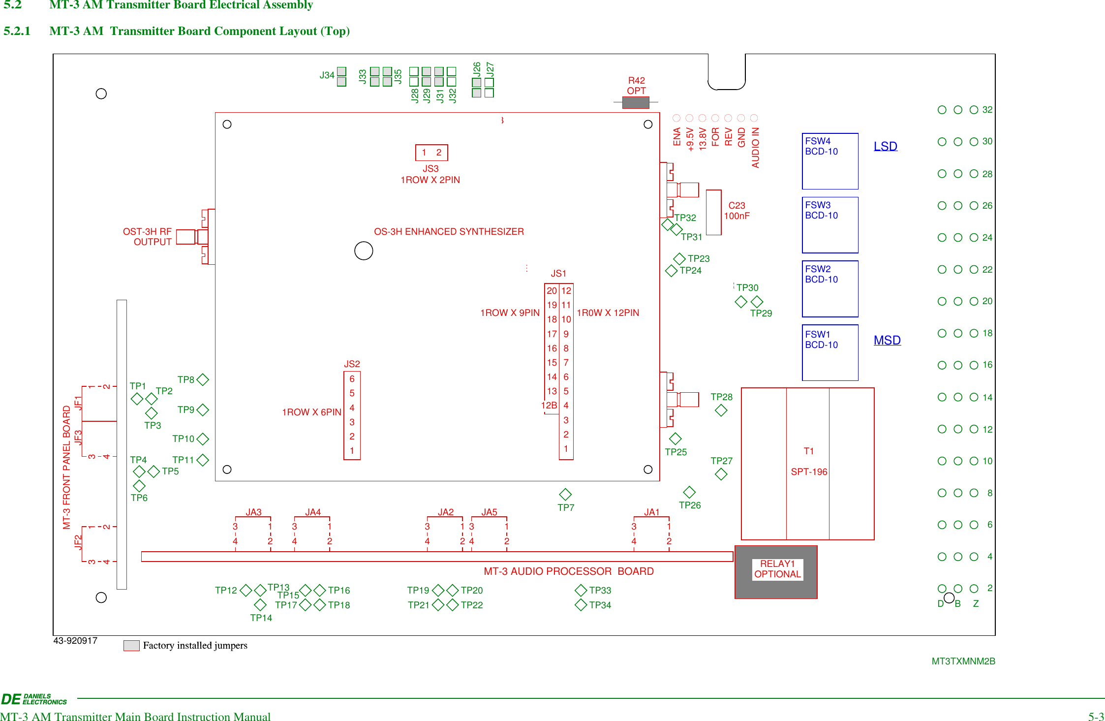
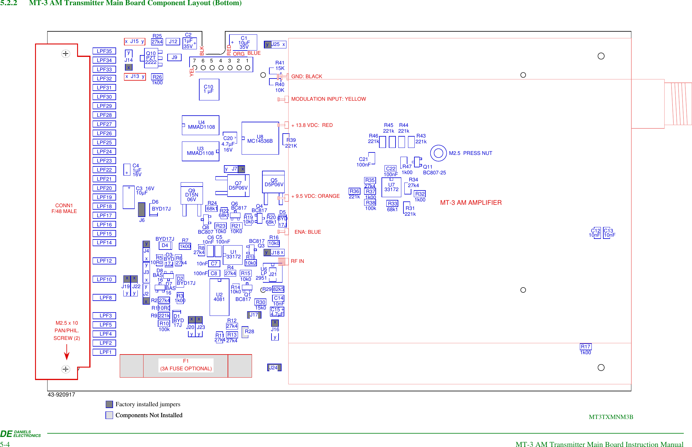
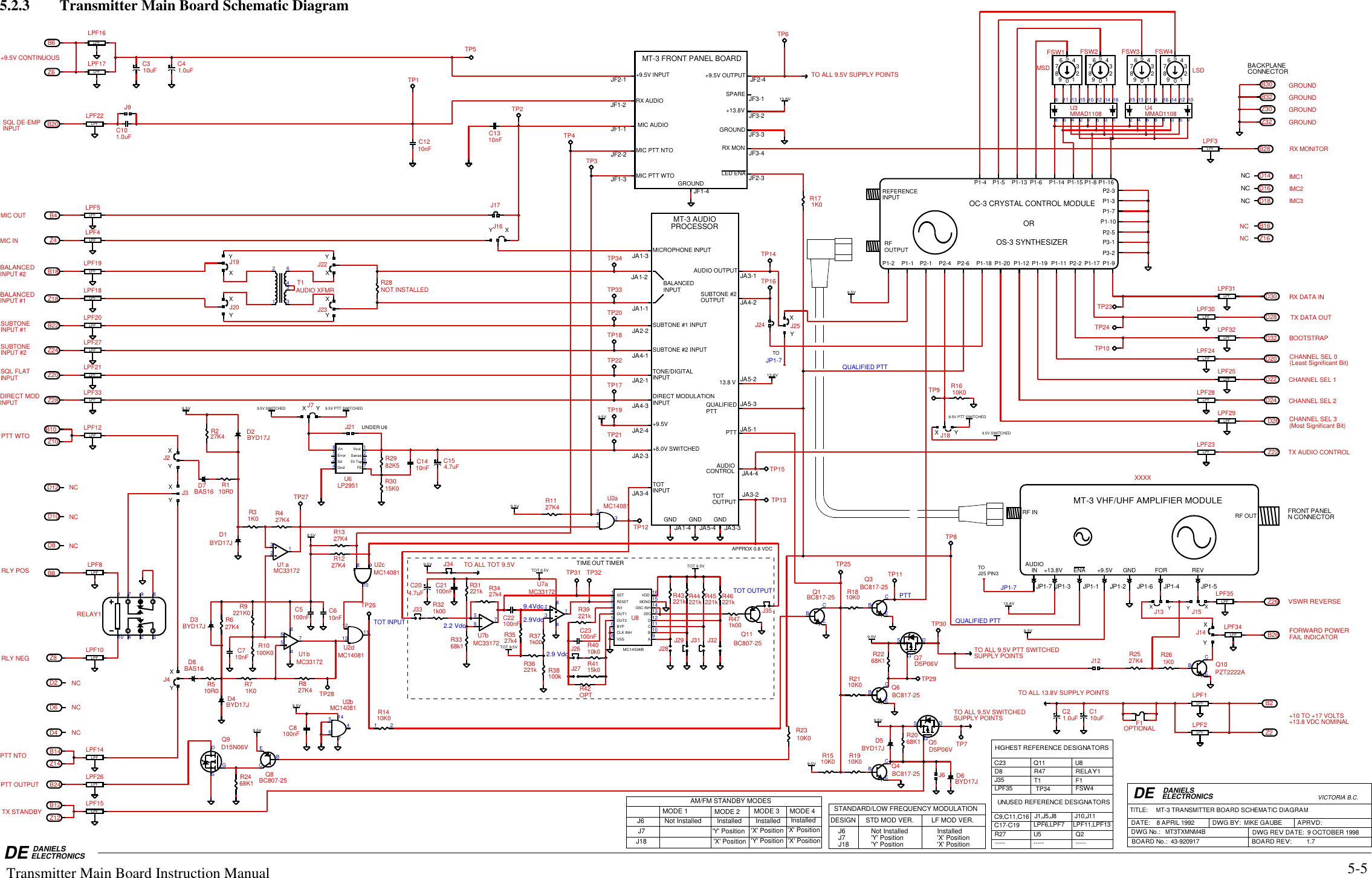
Codan Radio Communications VT-3-150-SN VT-3/140-SN & VT-3/160-SN VHF TRANSMITTERS User Manual IM21 VT3150AMP VHF Tx Amplifier Manual
Codan Radio Communications VT-3/140-SN & VT-3/160-SN VHF TRANSMITTERS IM21 VT3150AMP VHF Tx Amplifier Manual
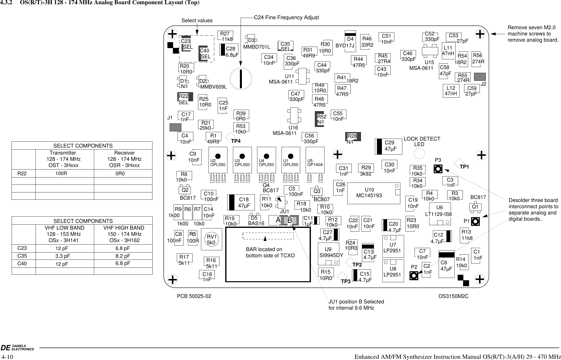
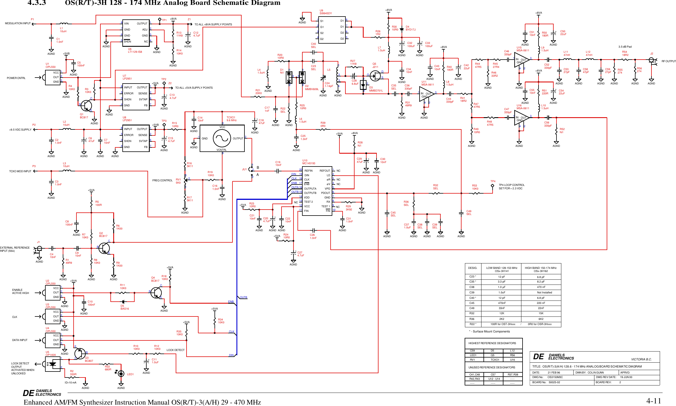
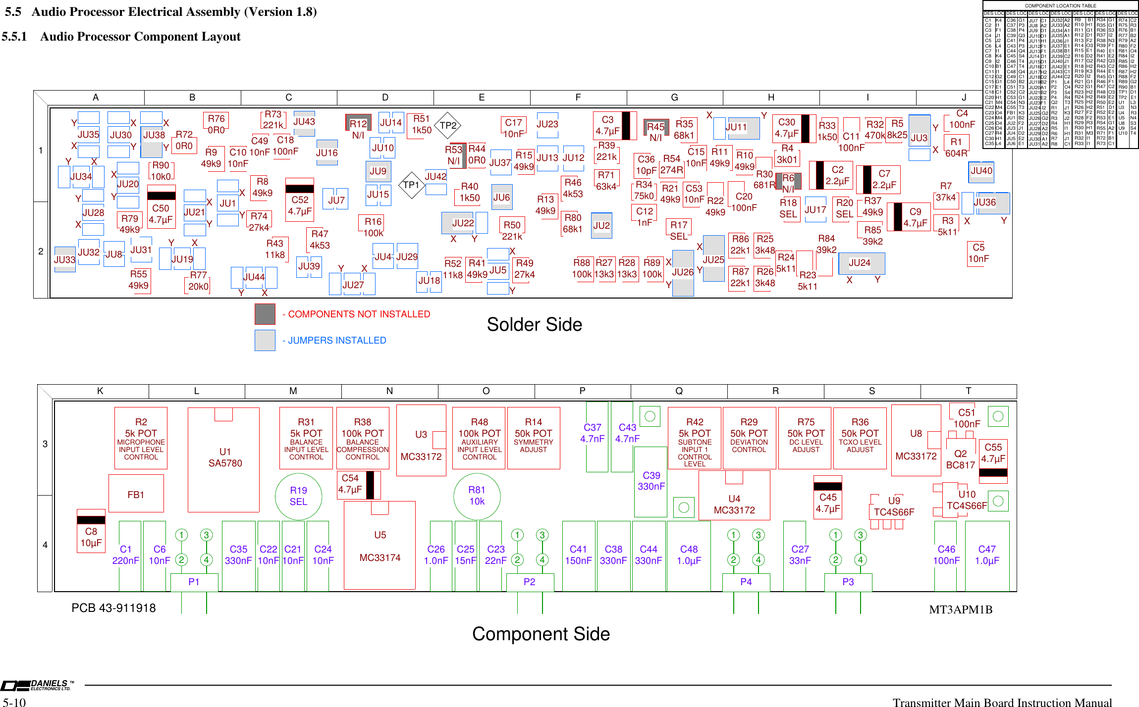
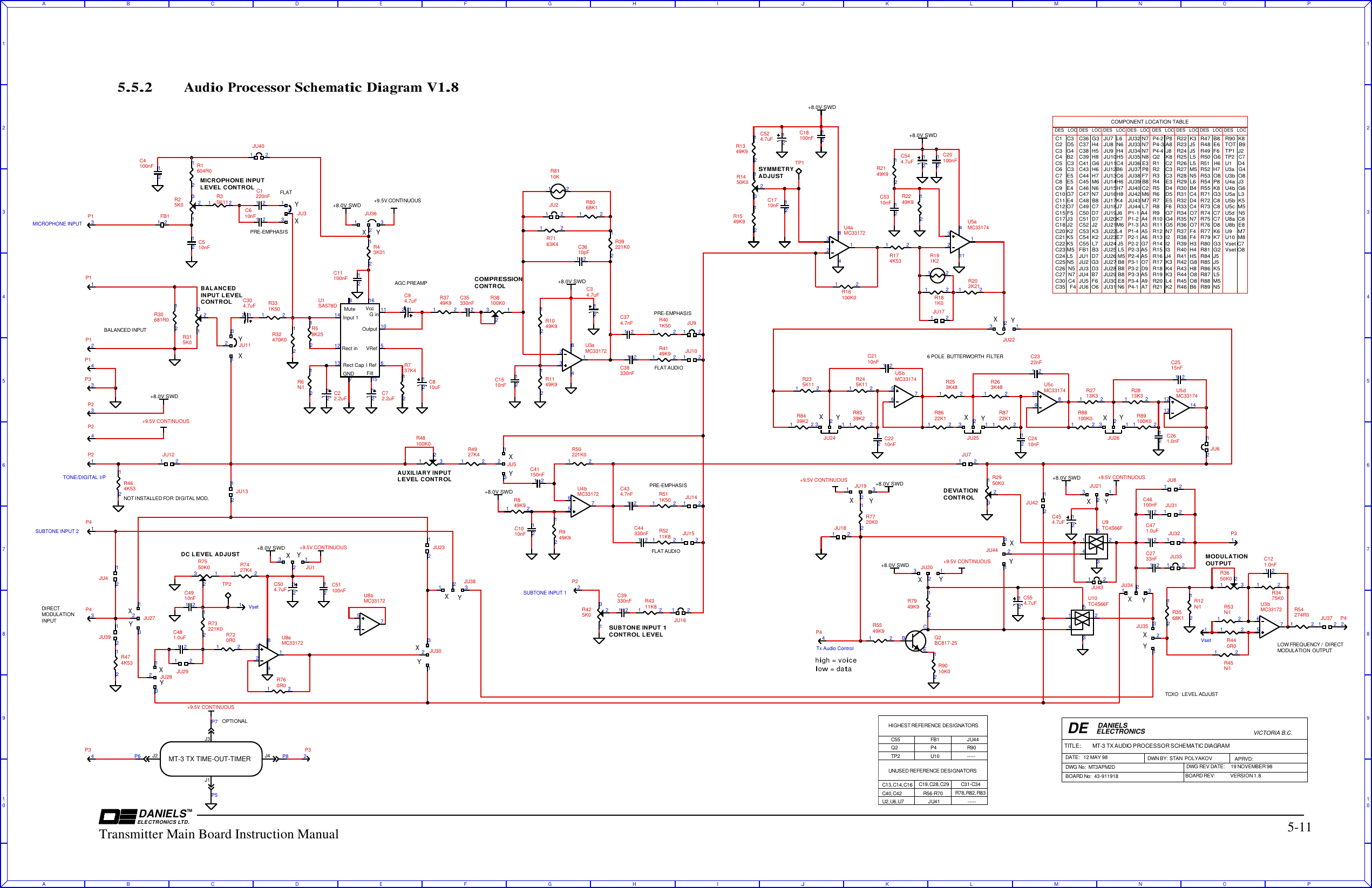
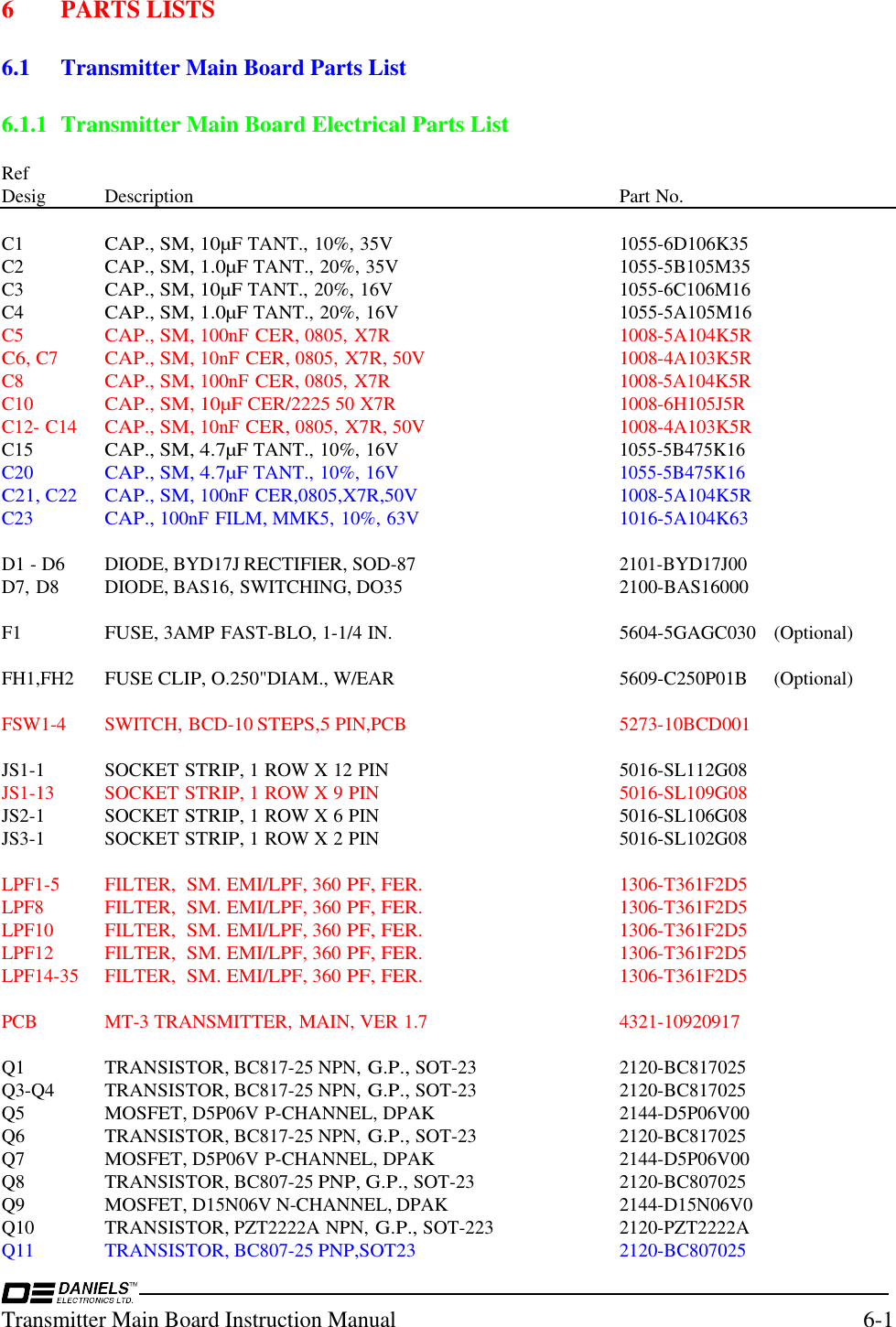
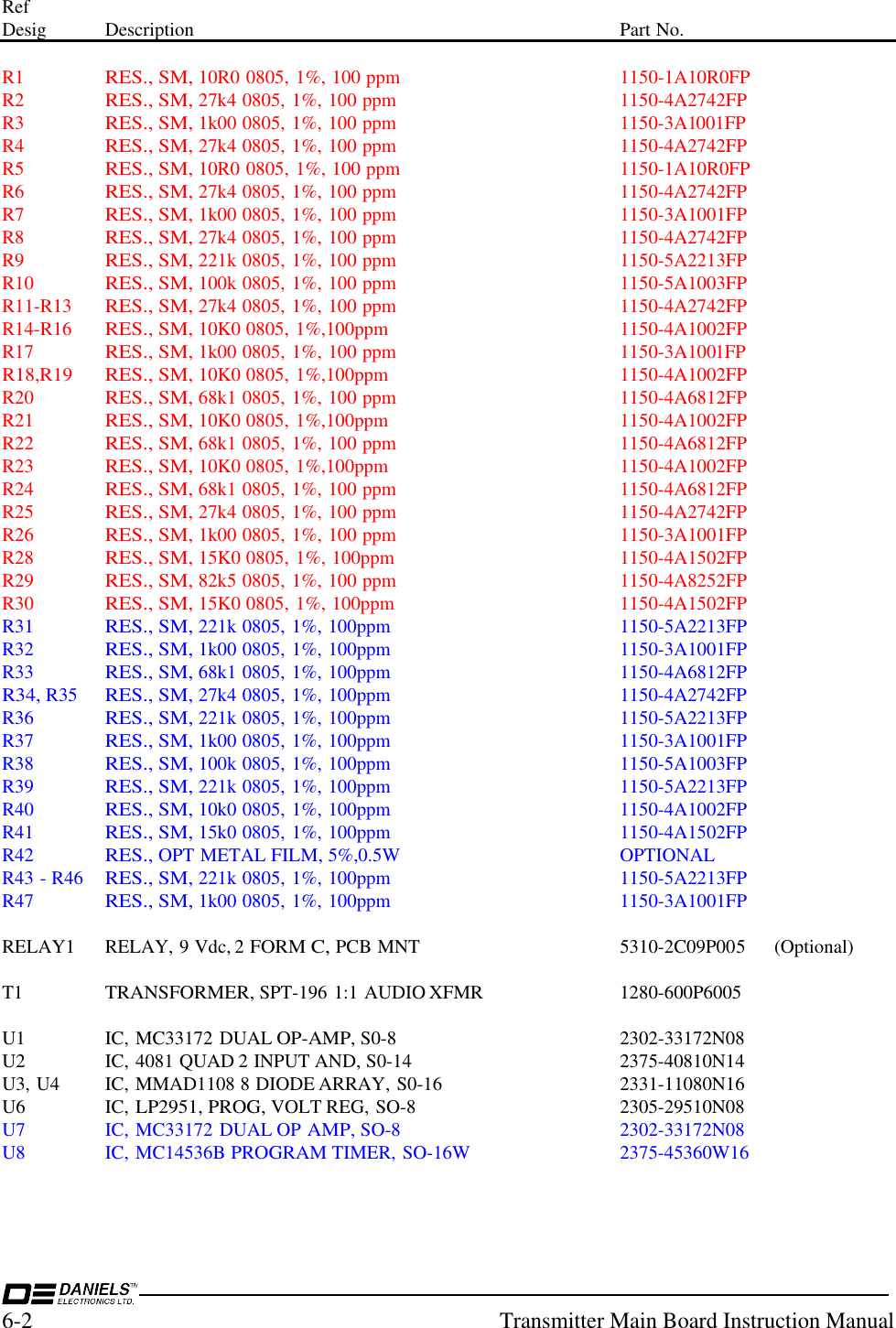
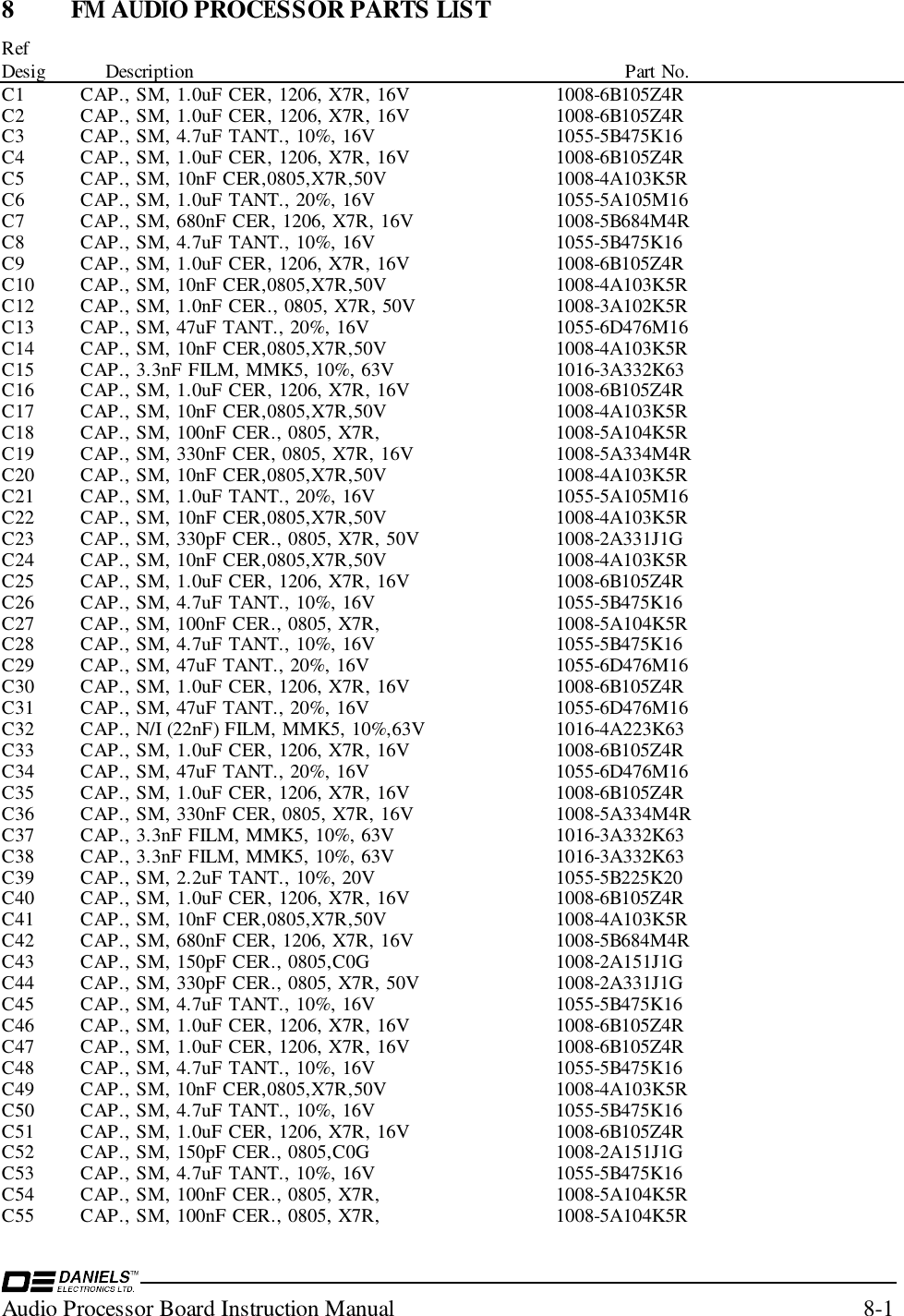
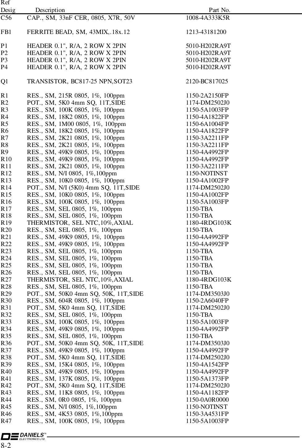
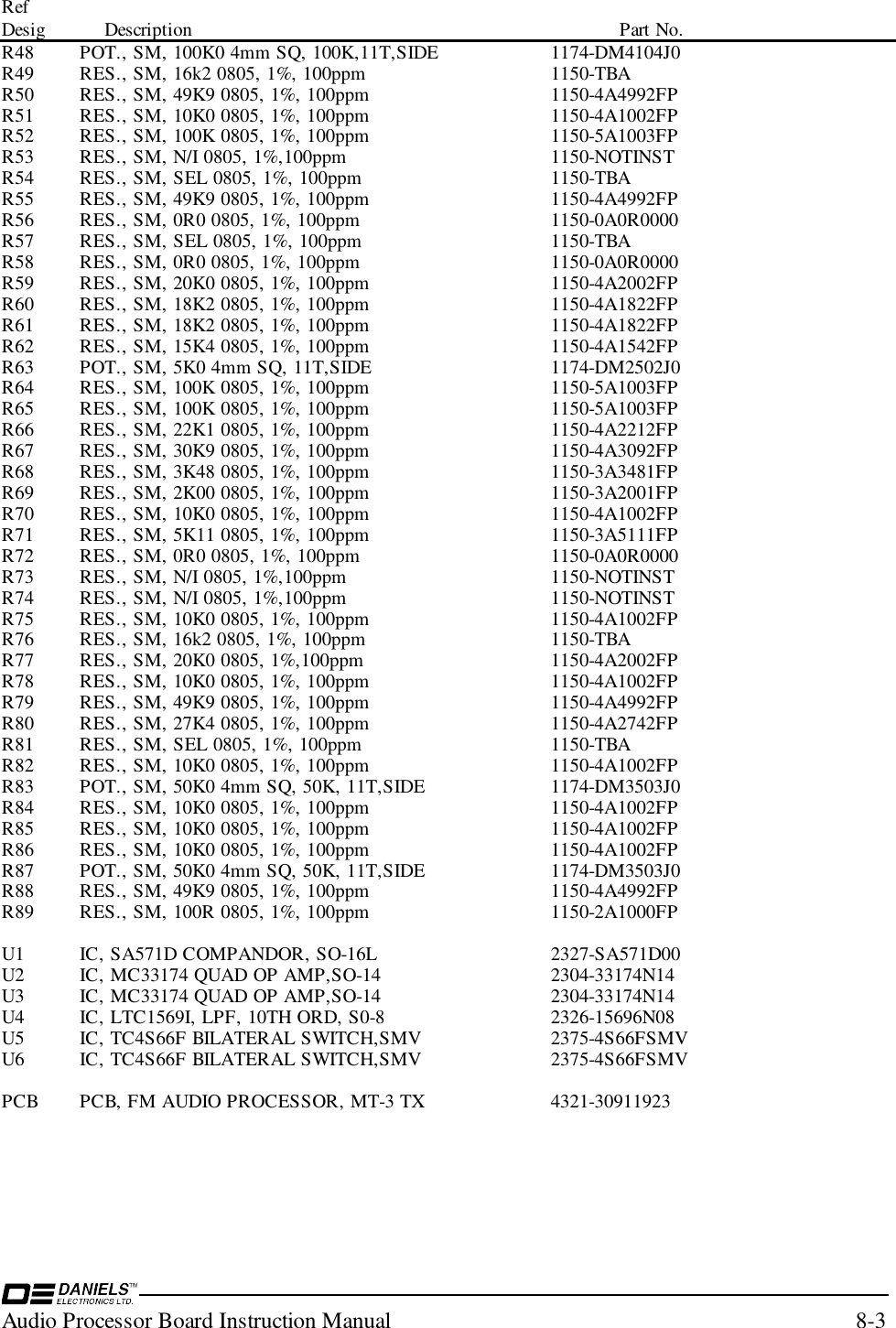
VHF Tx Manual including schematics and parts list
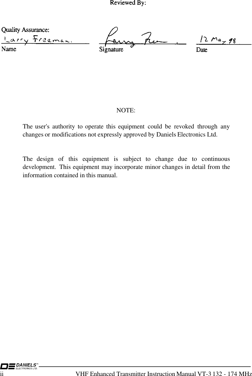

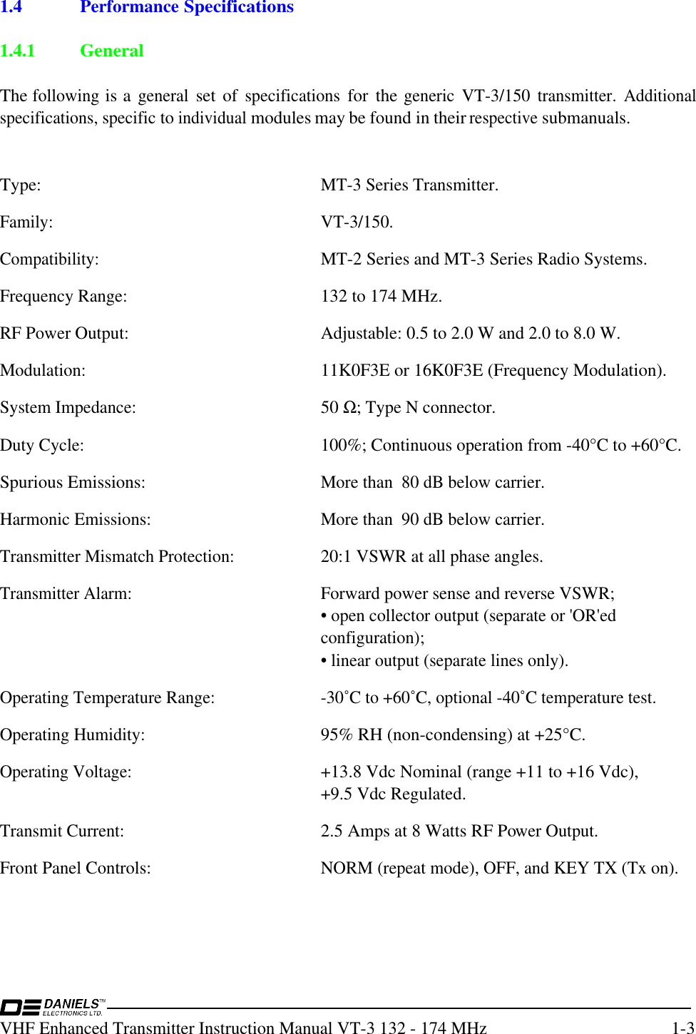
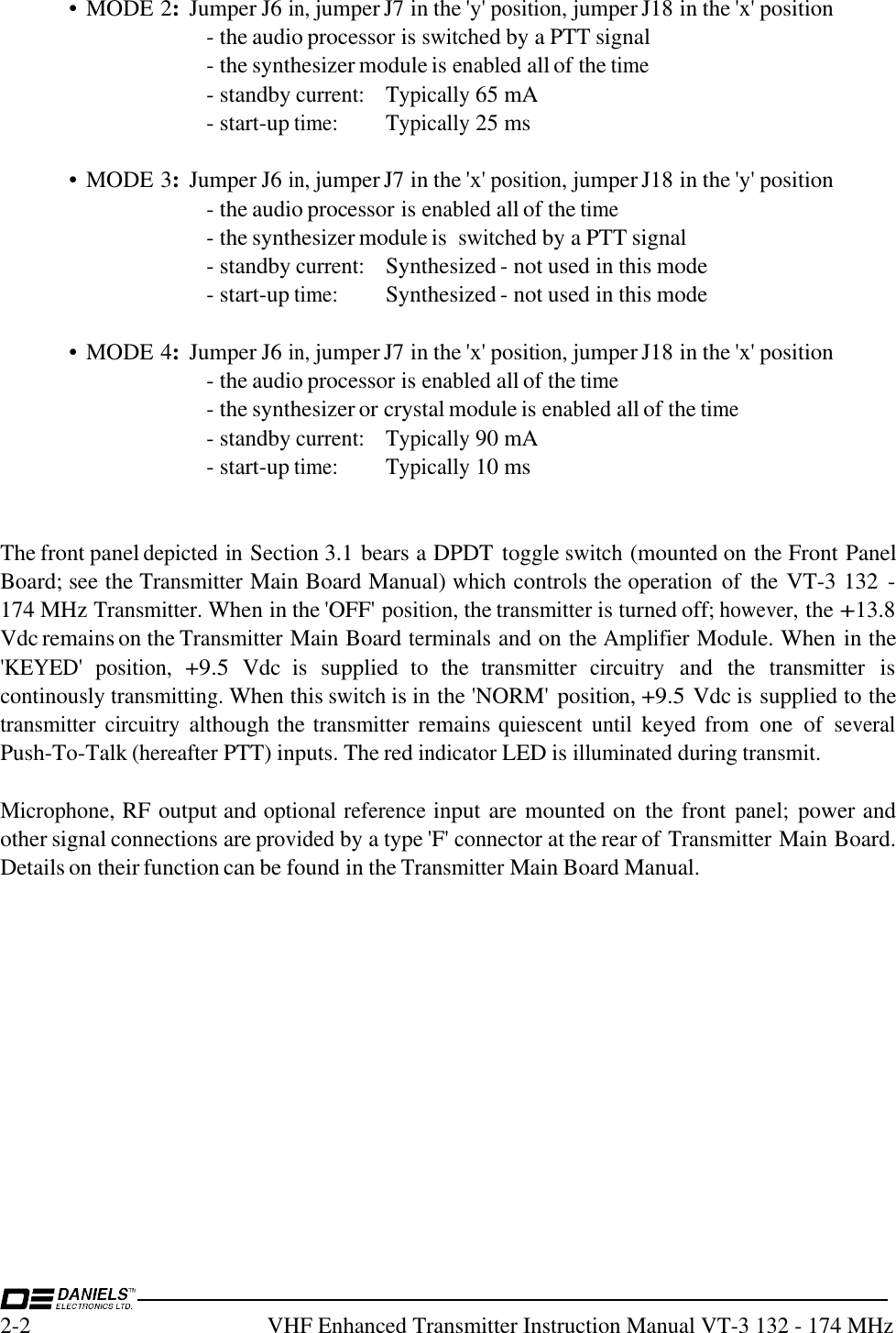
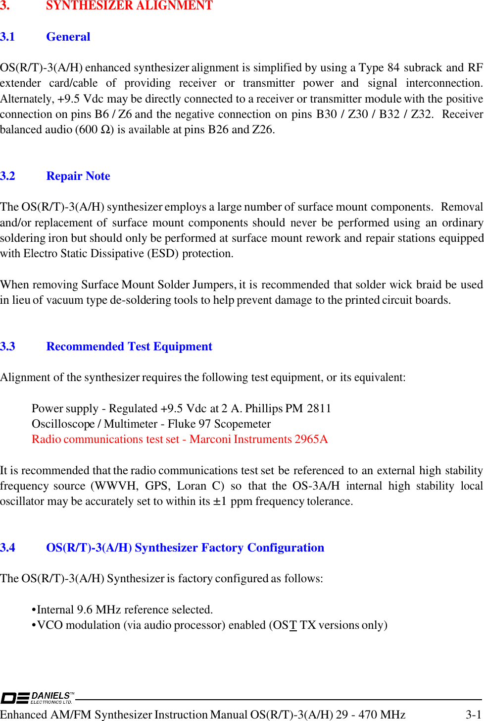
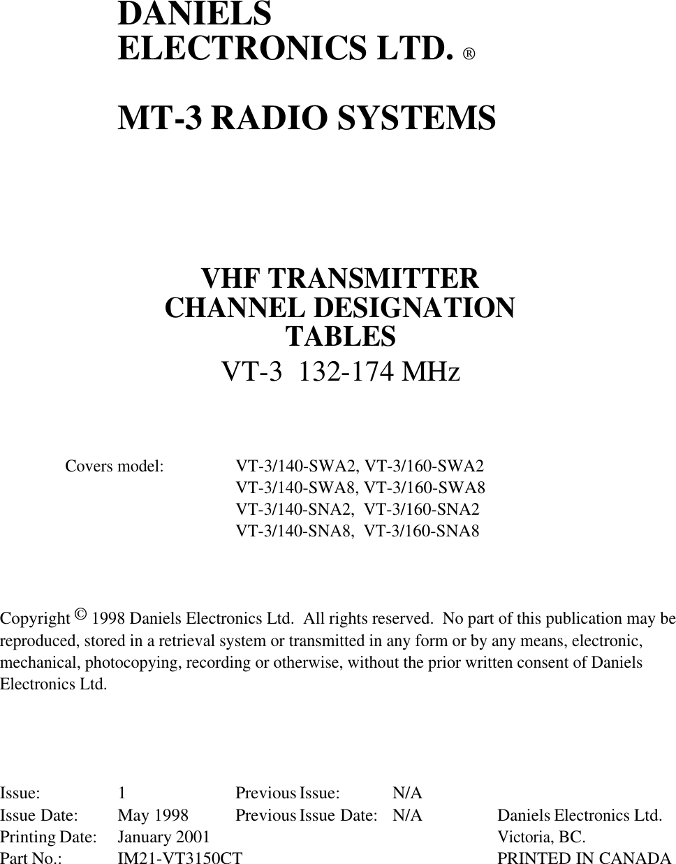
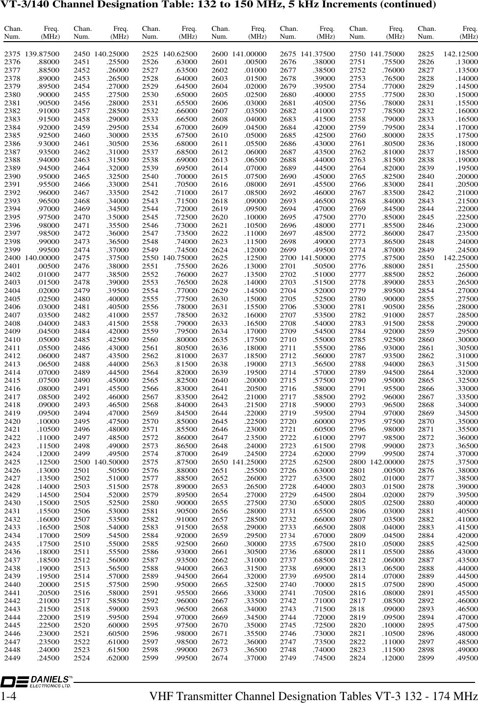
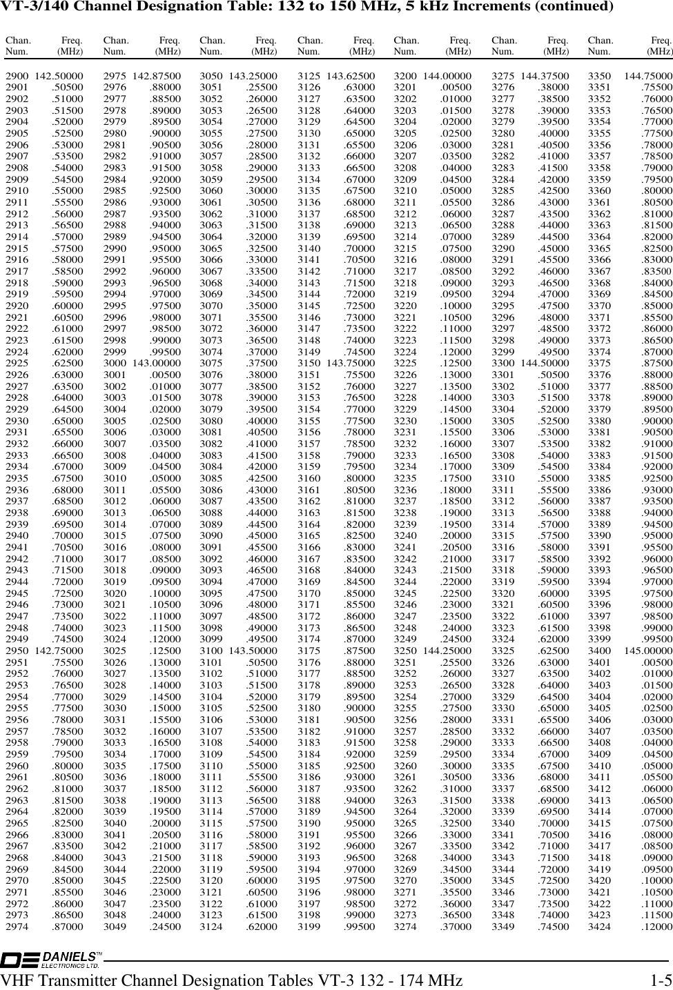
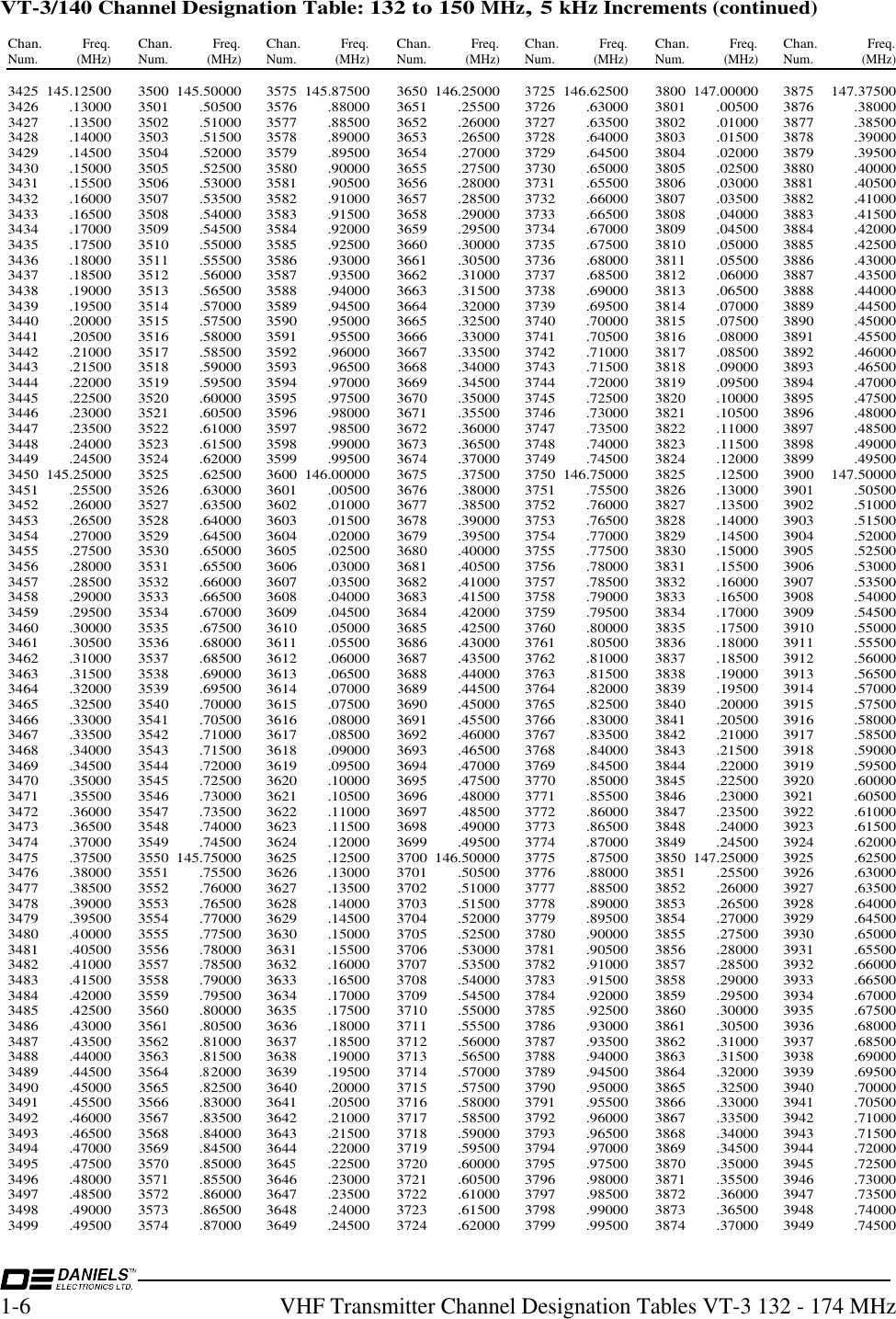
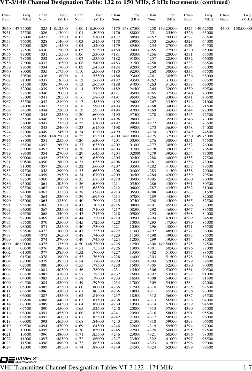
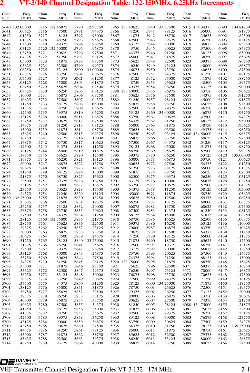
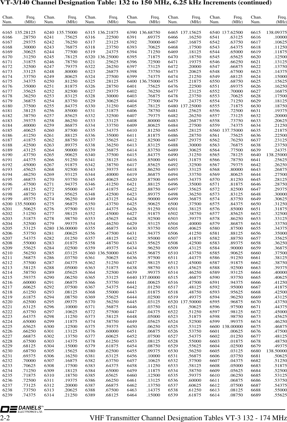
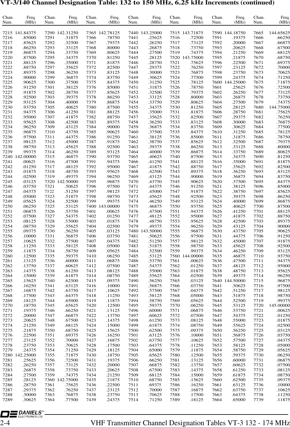
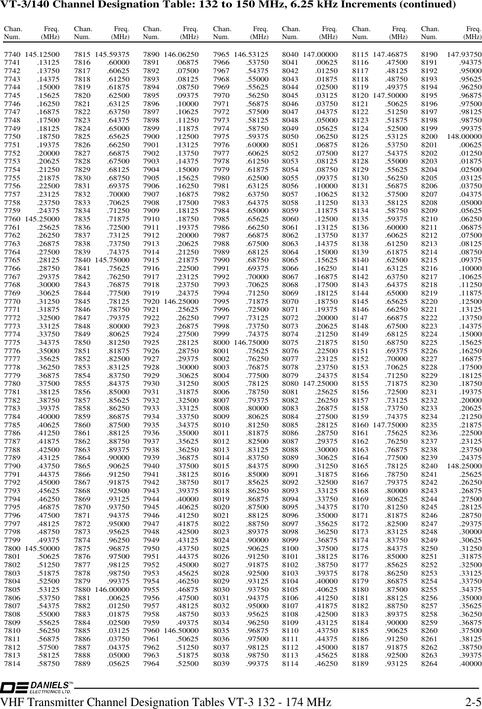
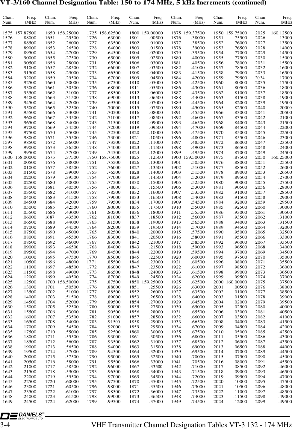
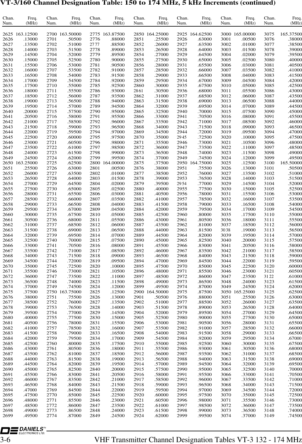
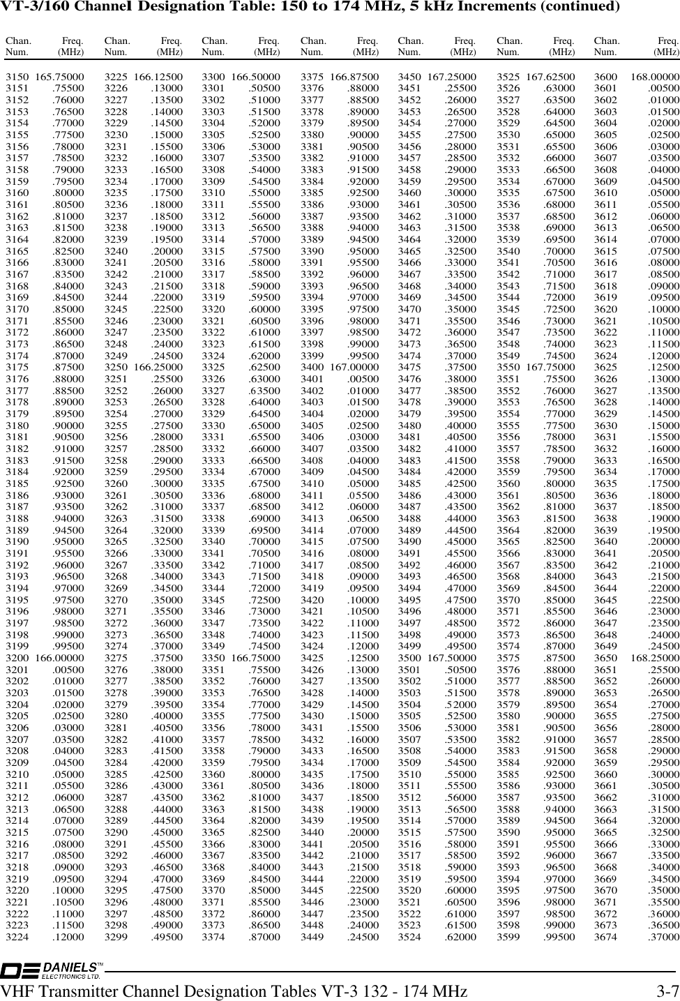
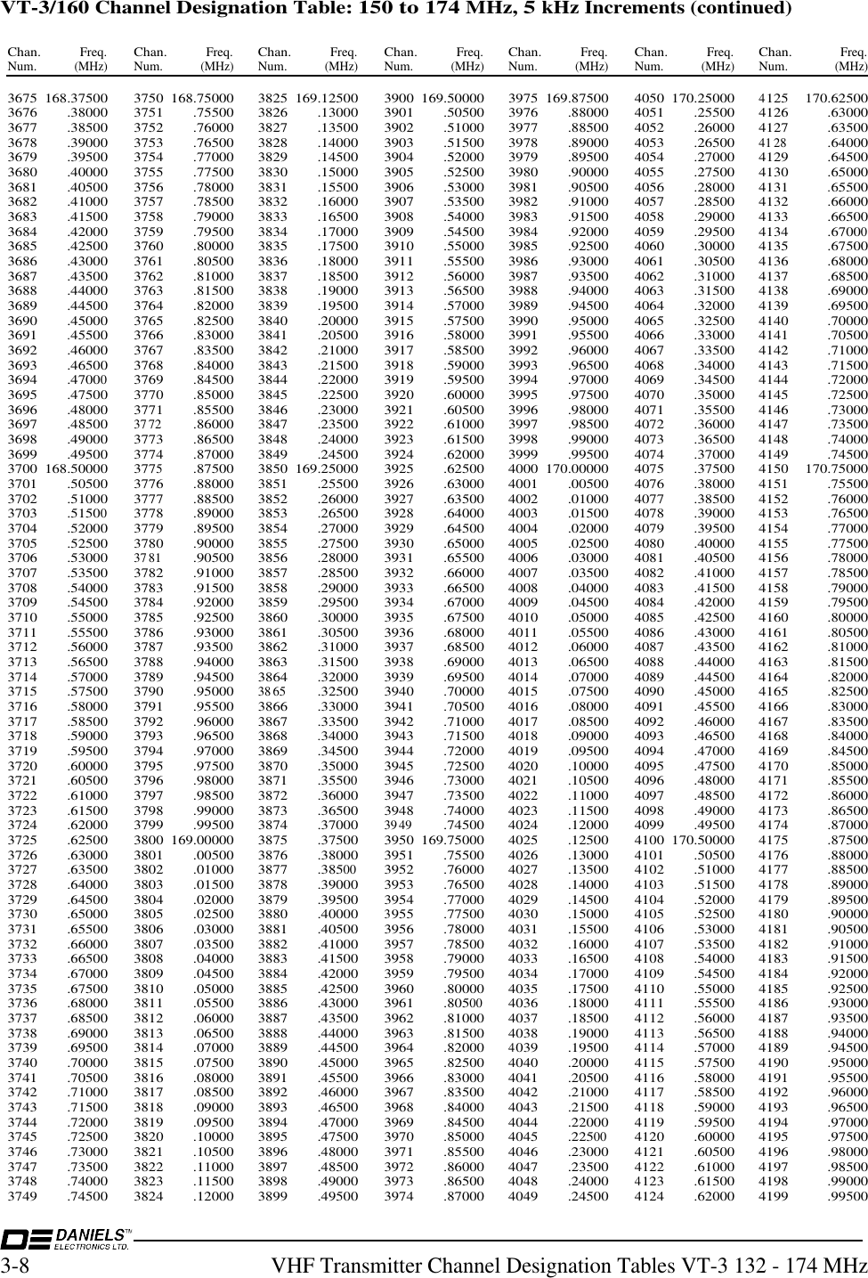
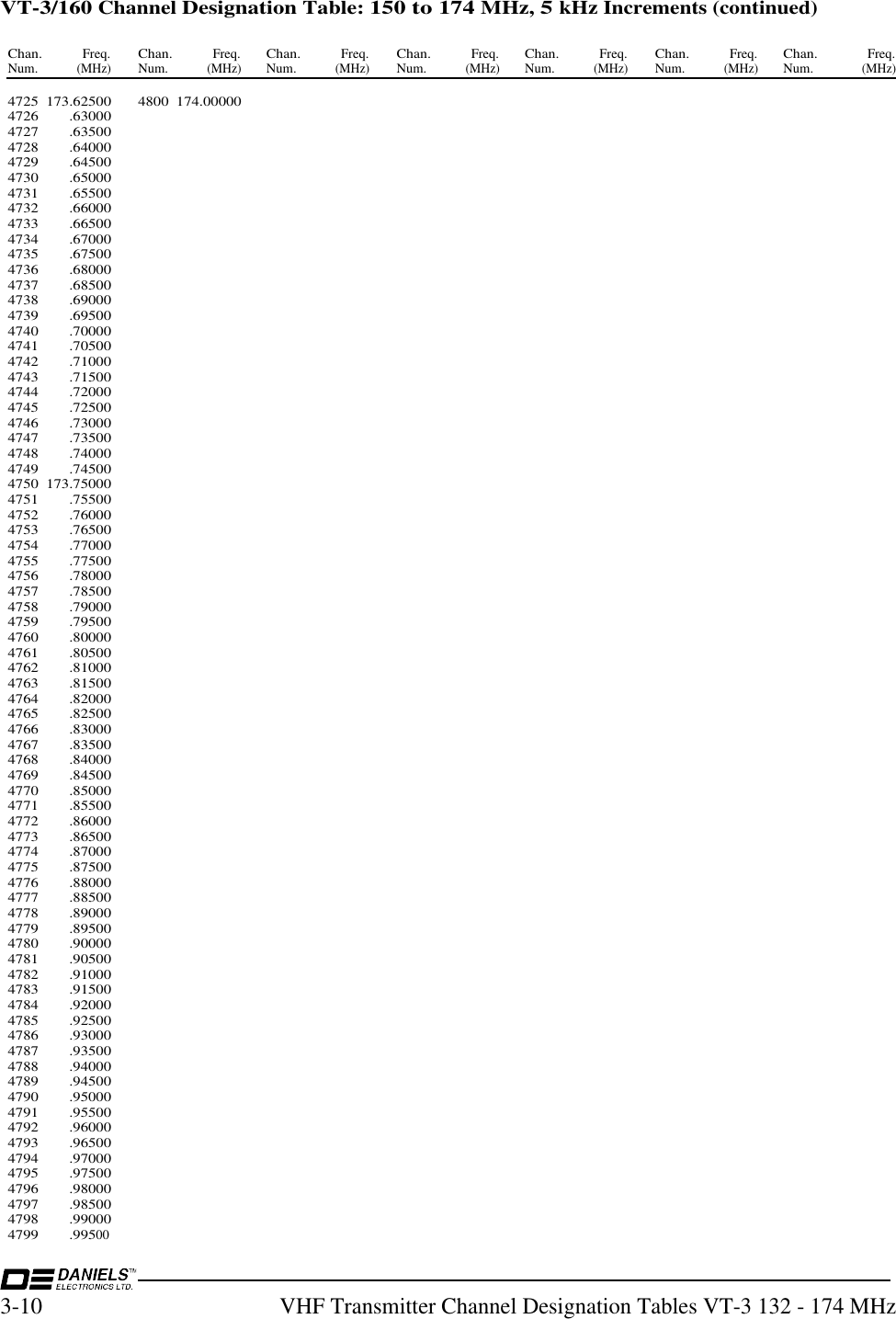
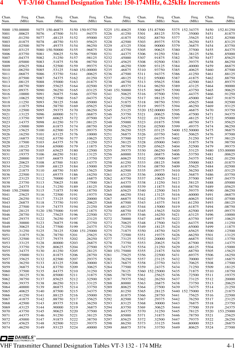
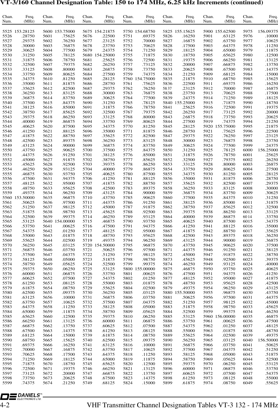
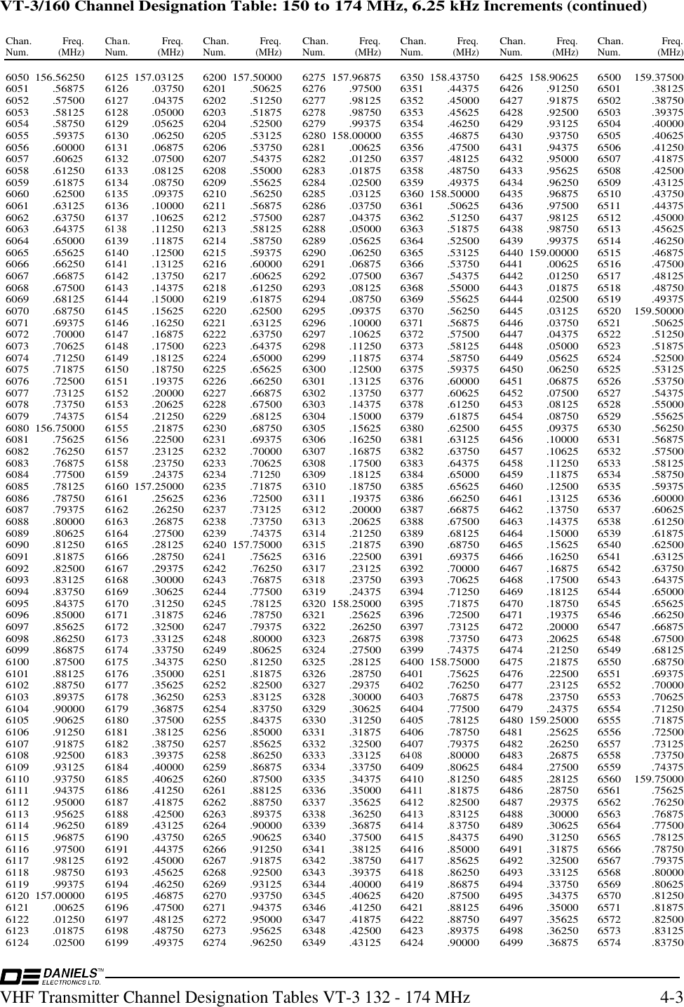
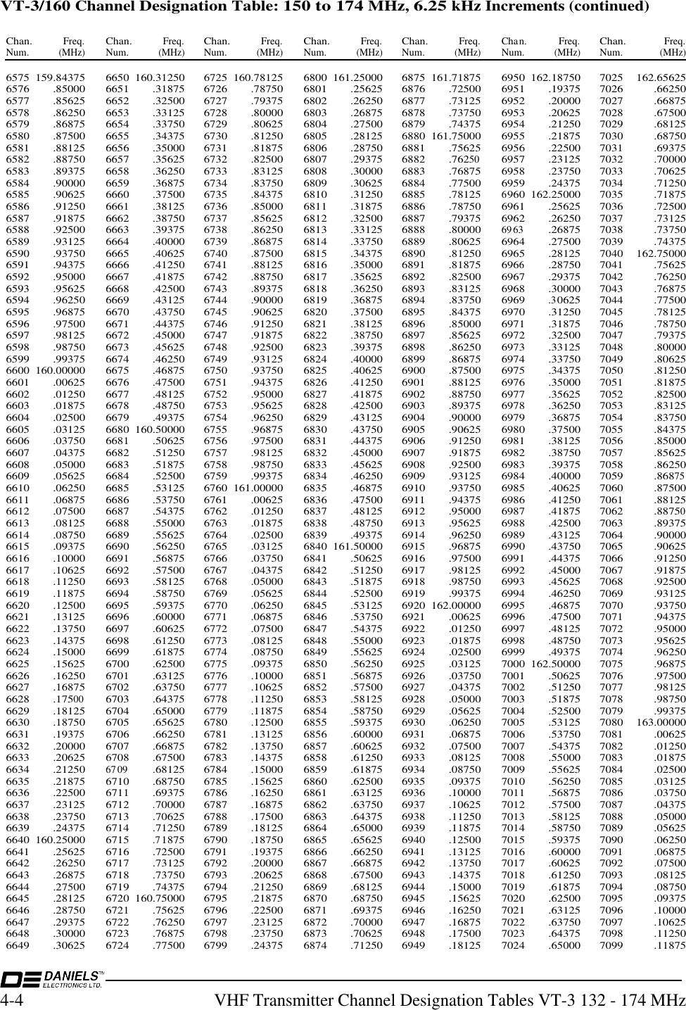
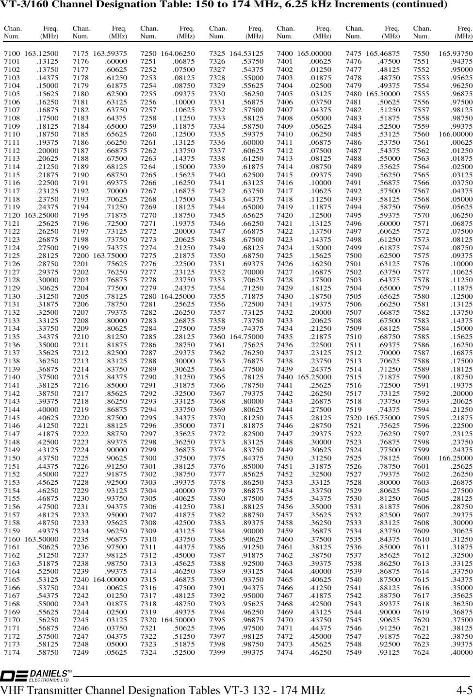
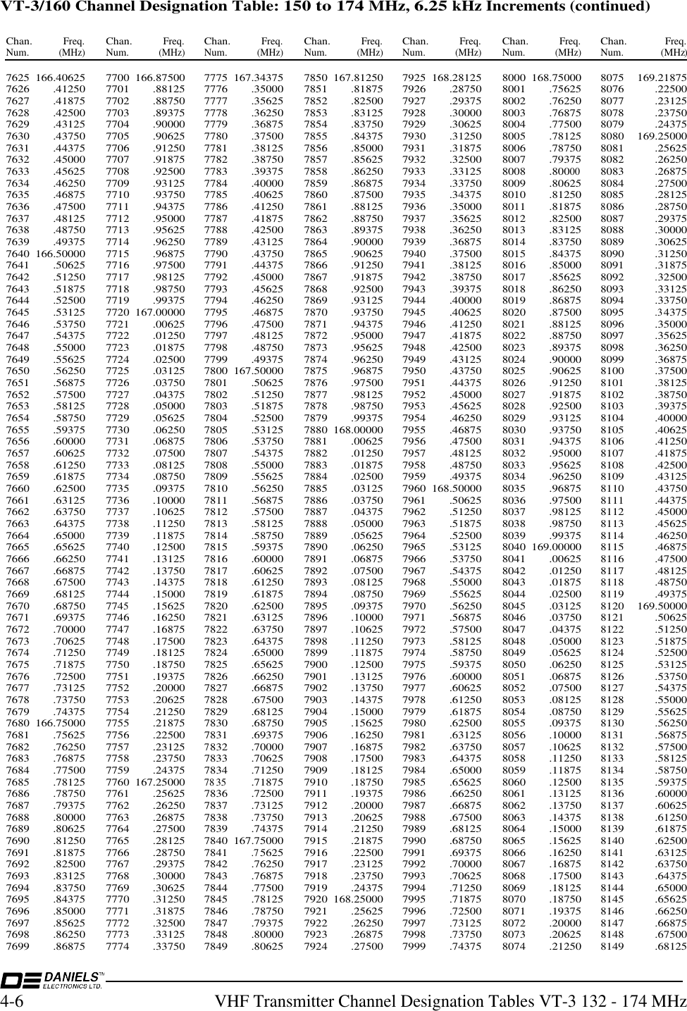
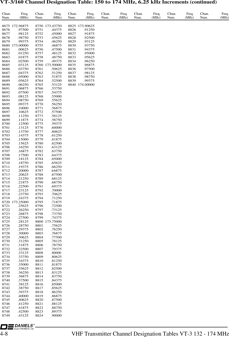
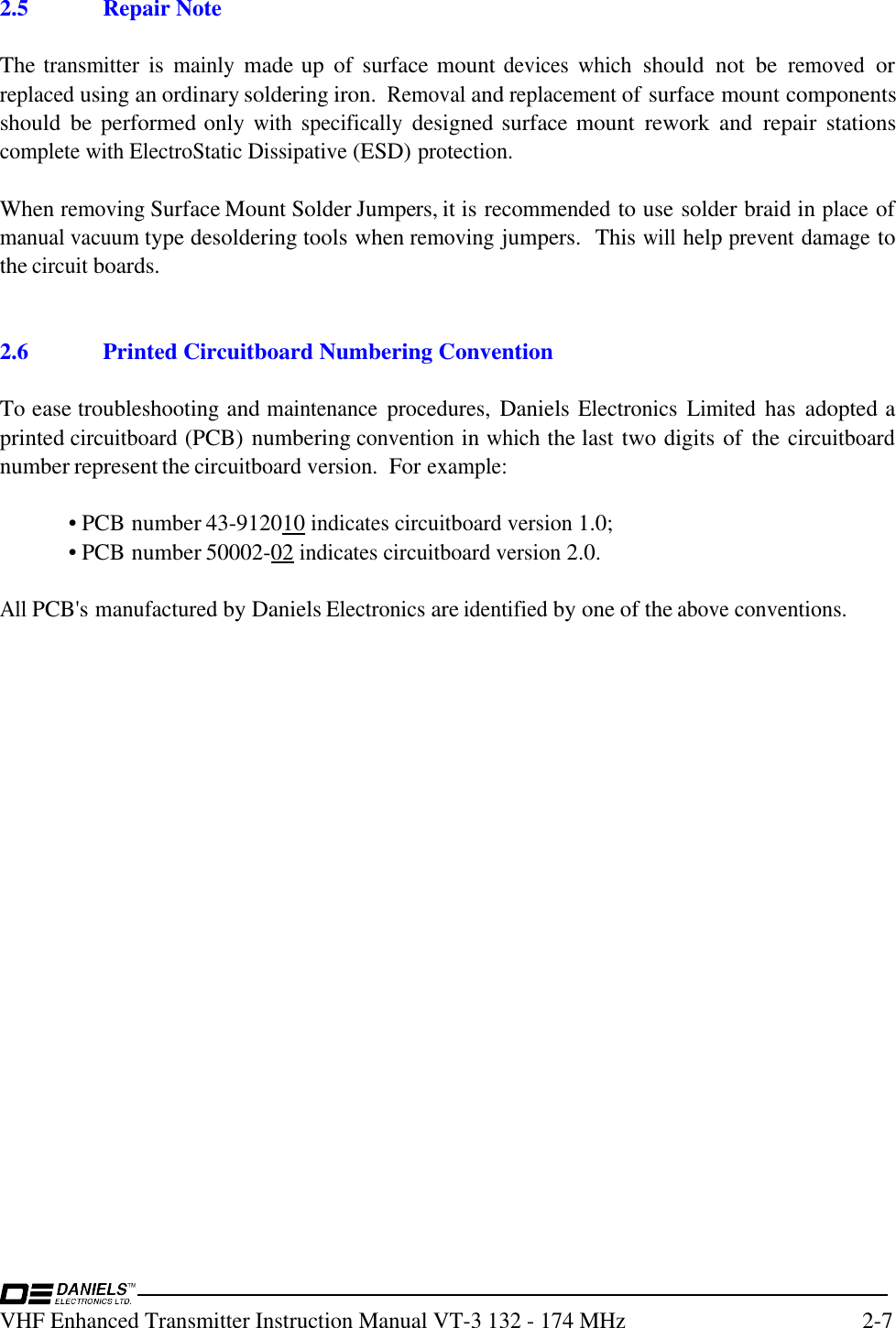
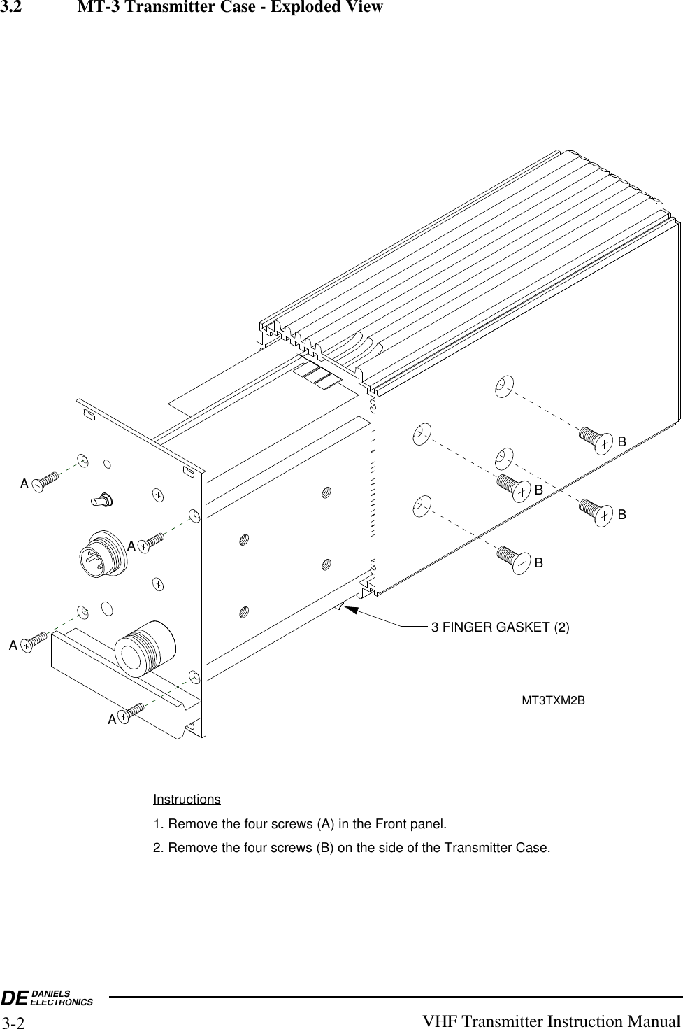
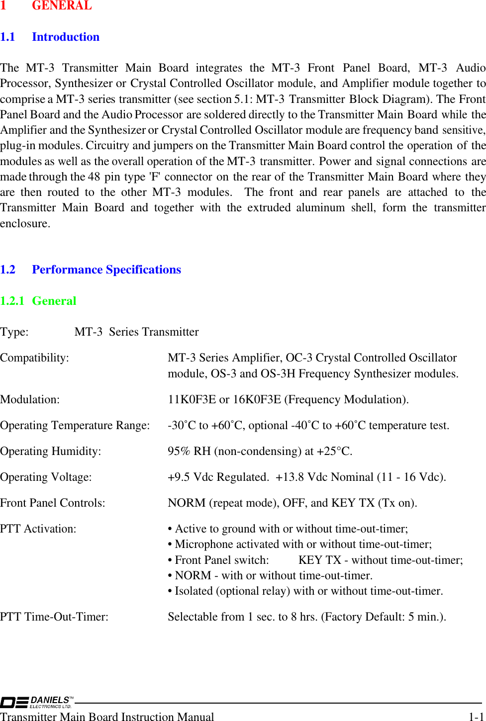
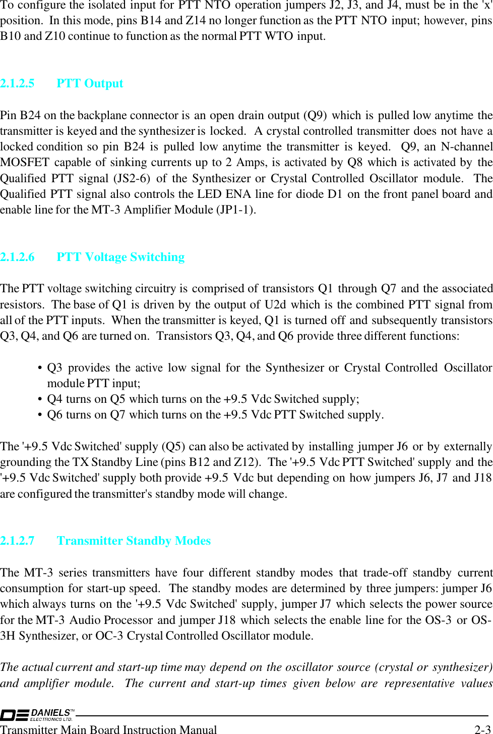
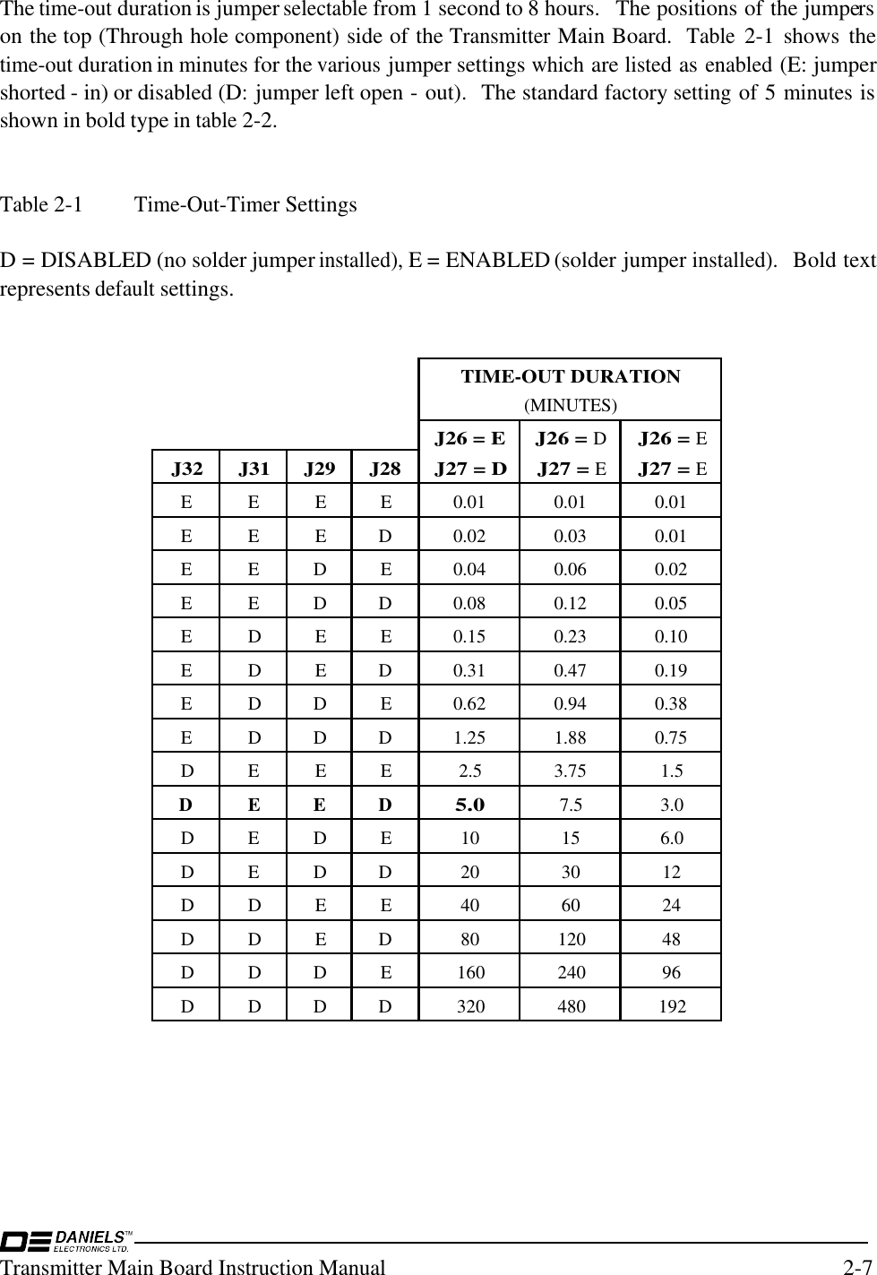
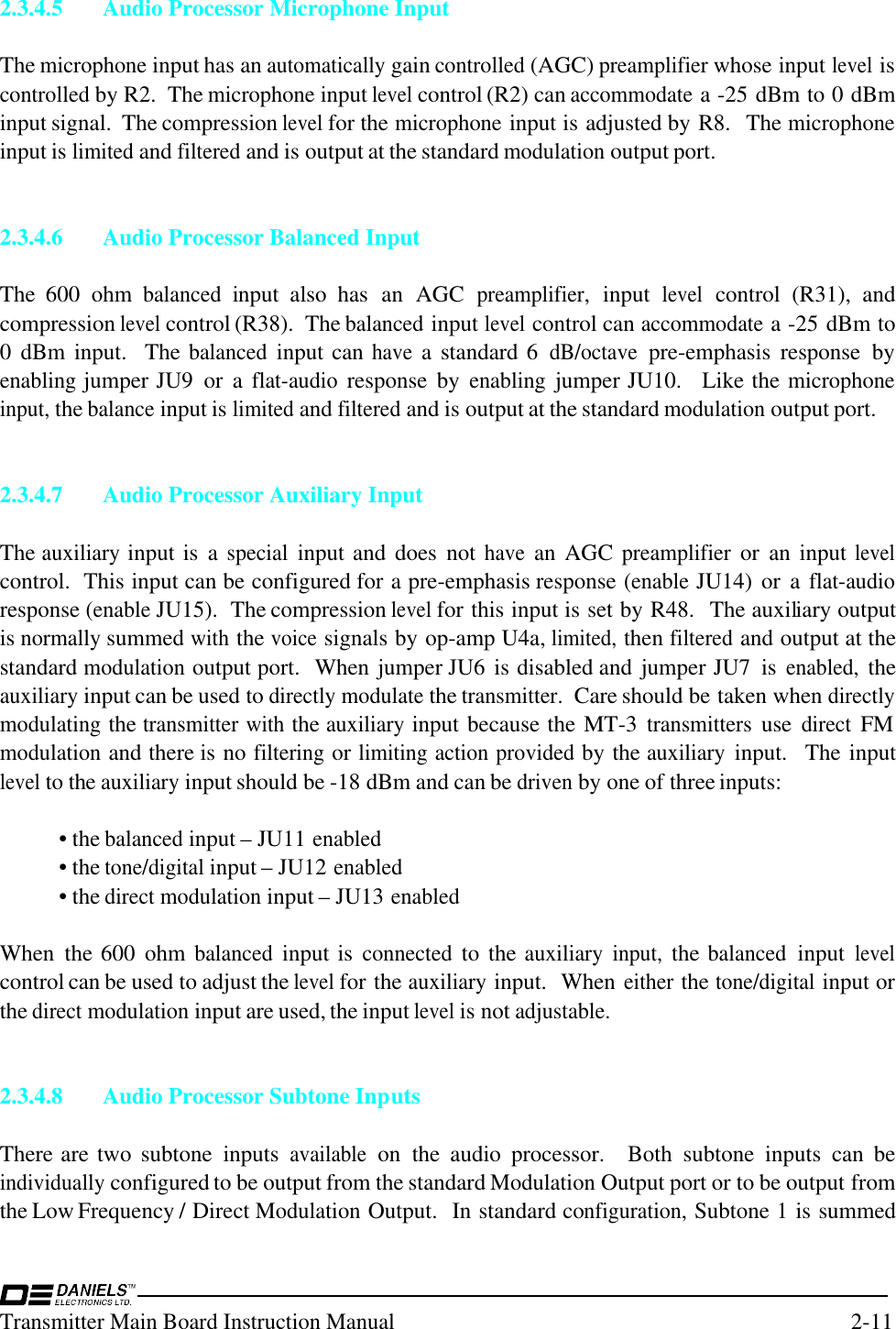
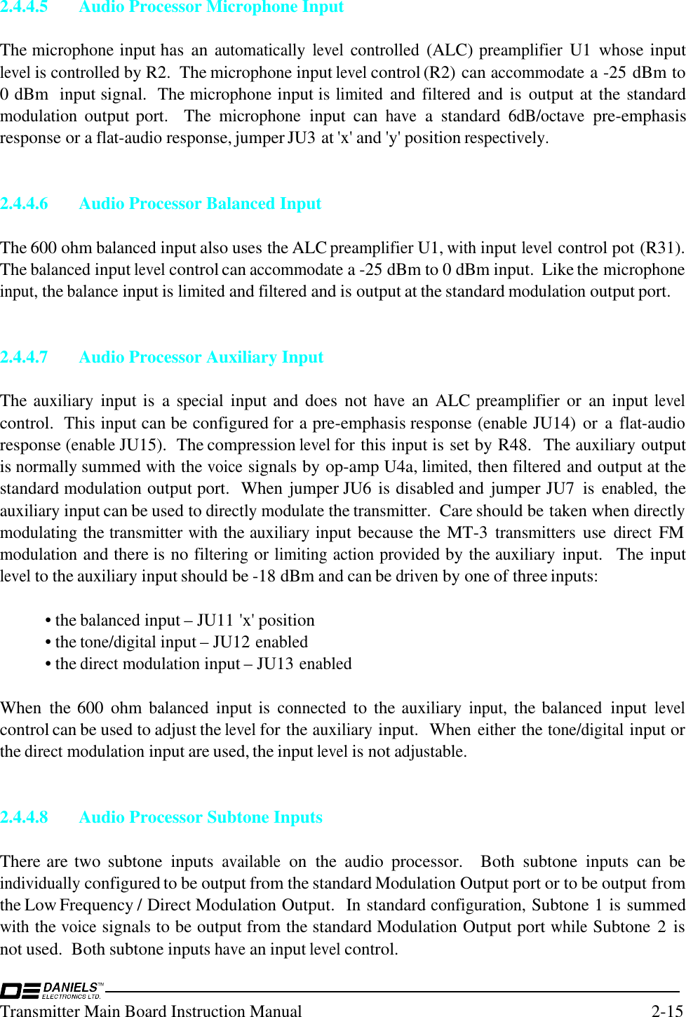
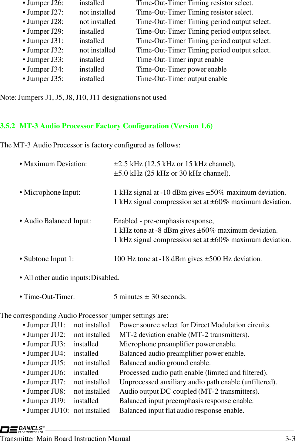
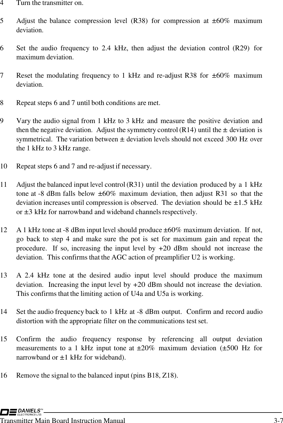
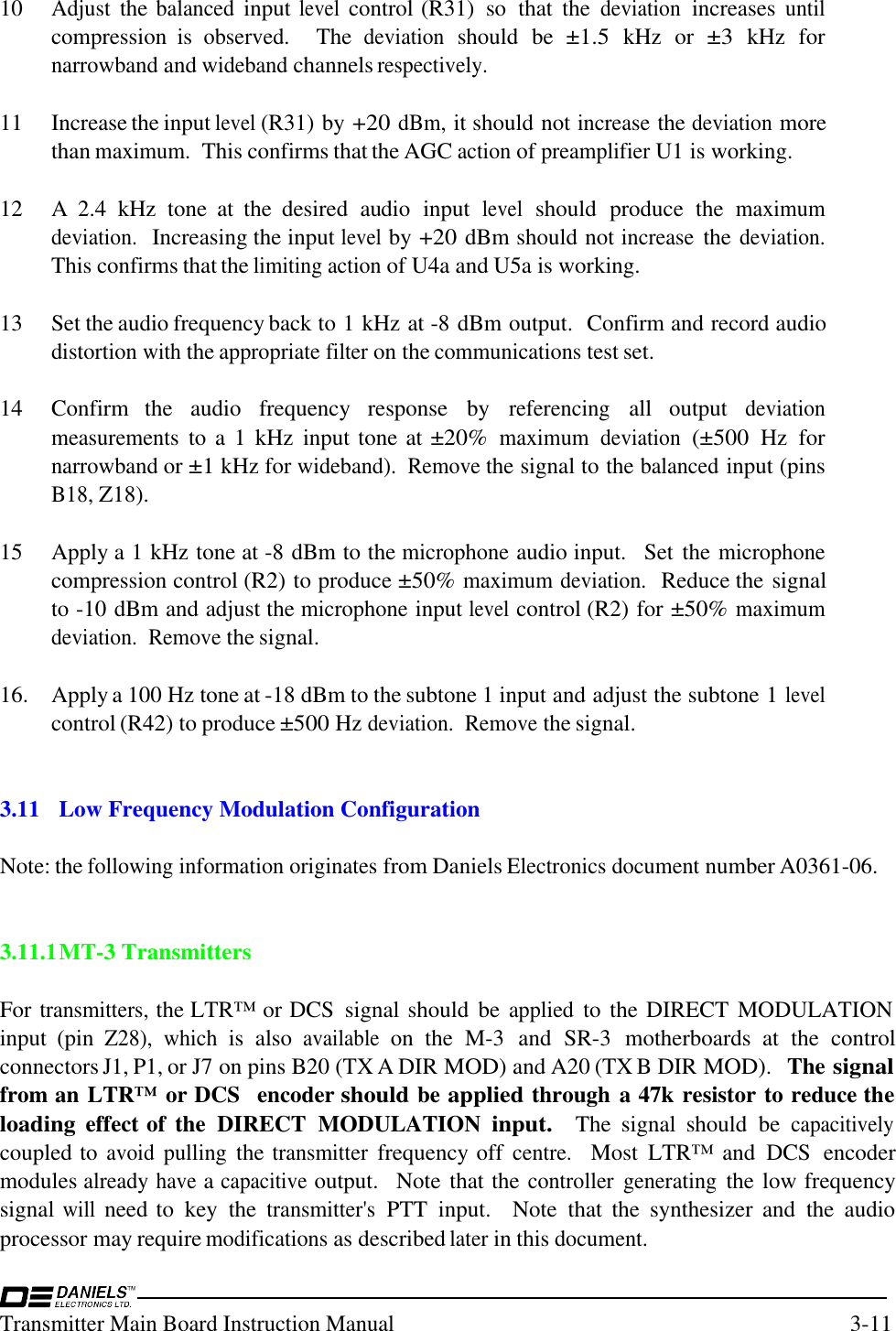
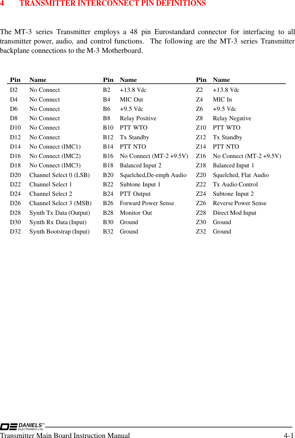
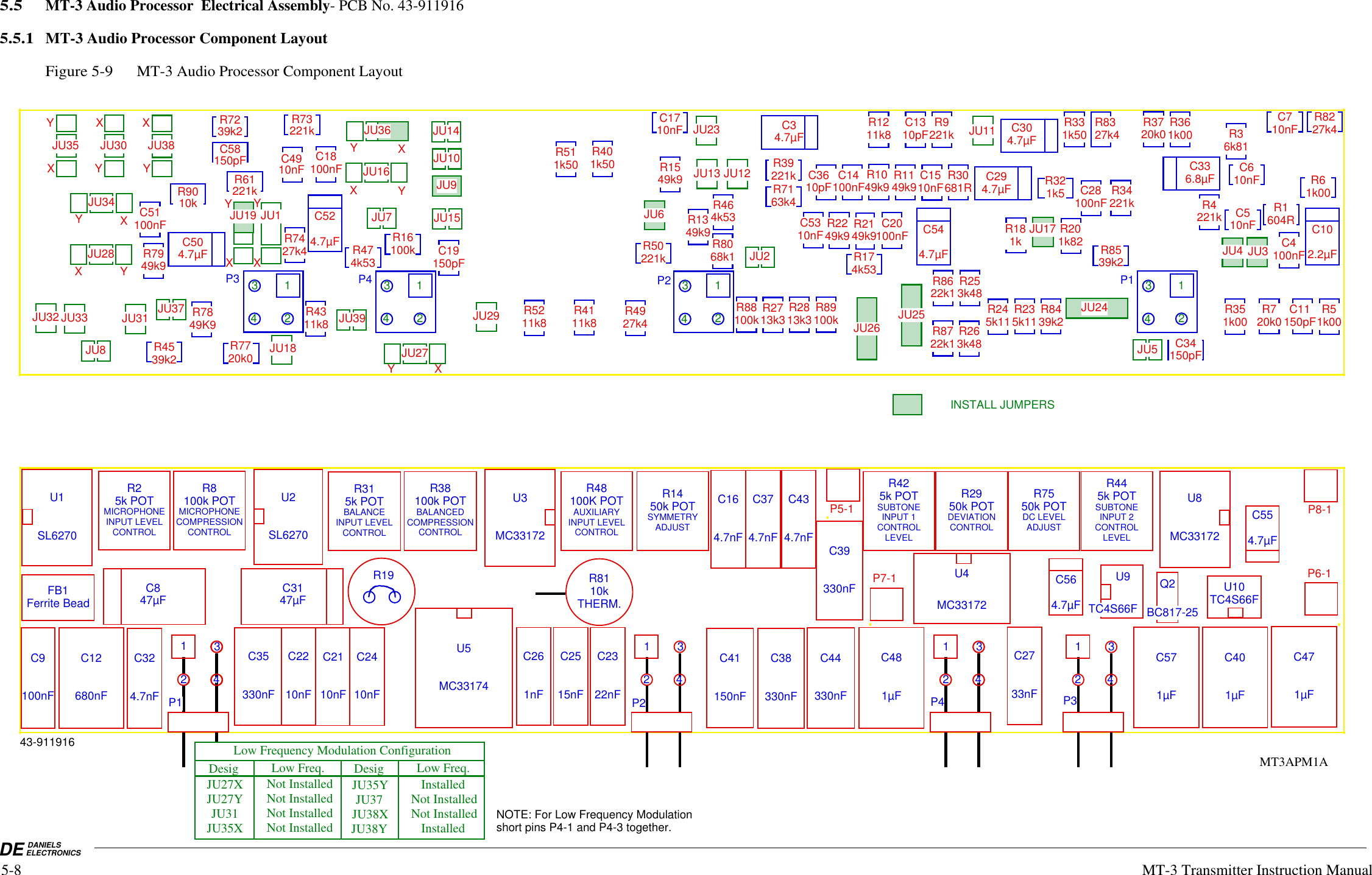
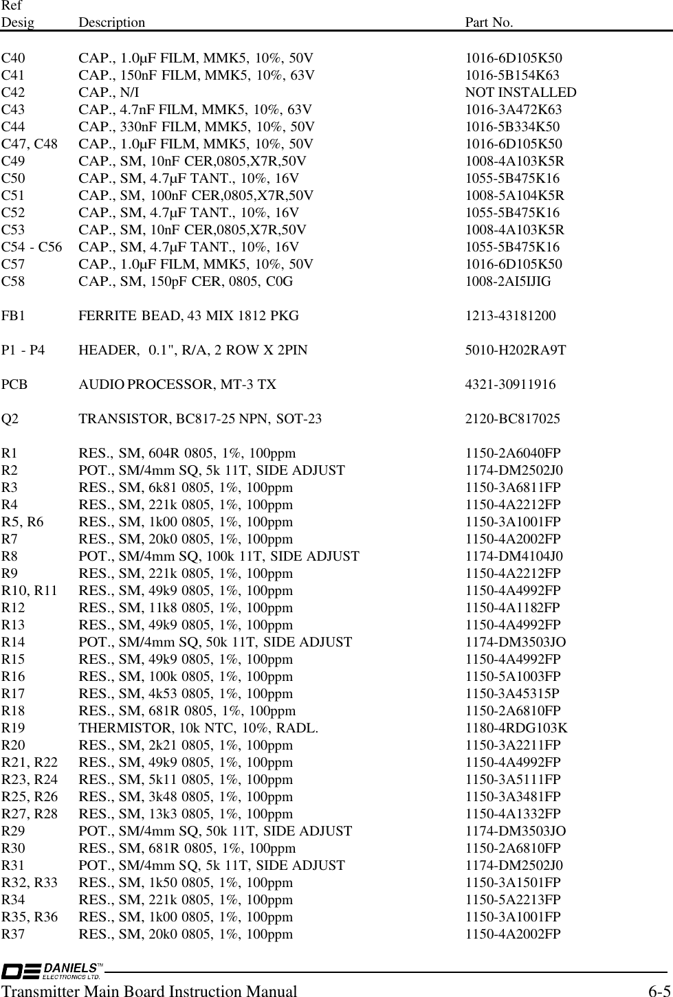
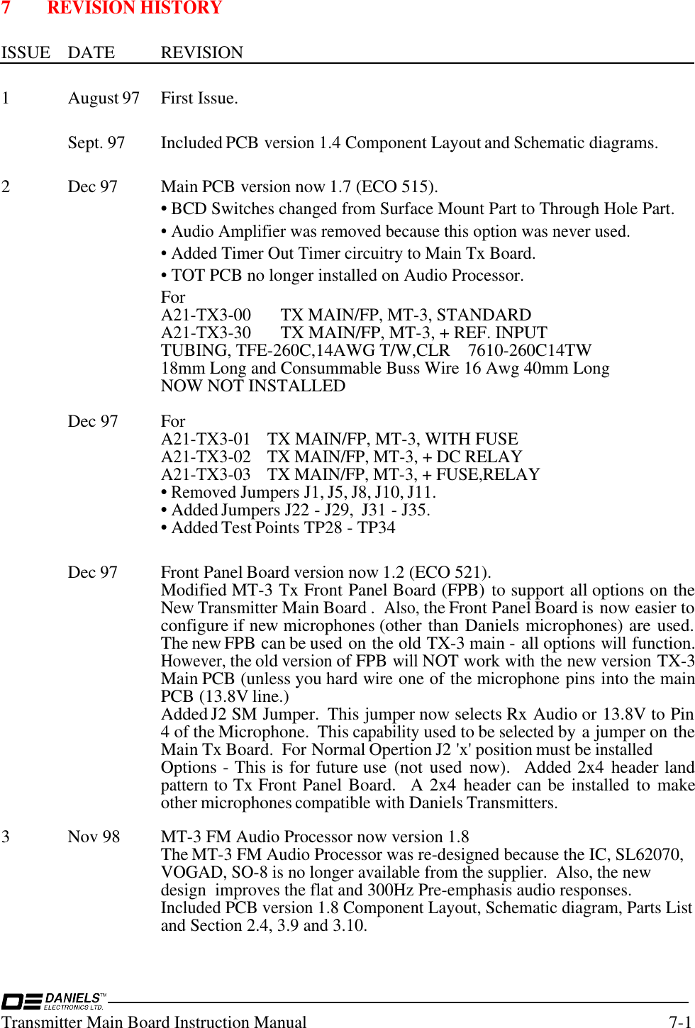
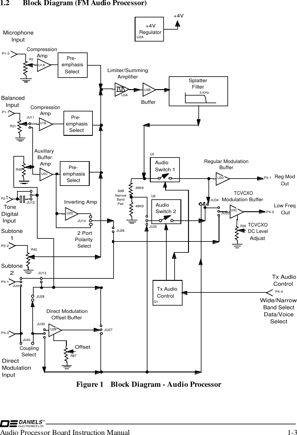
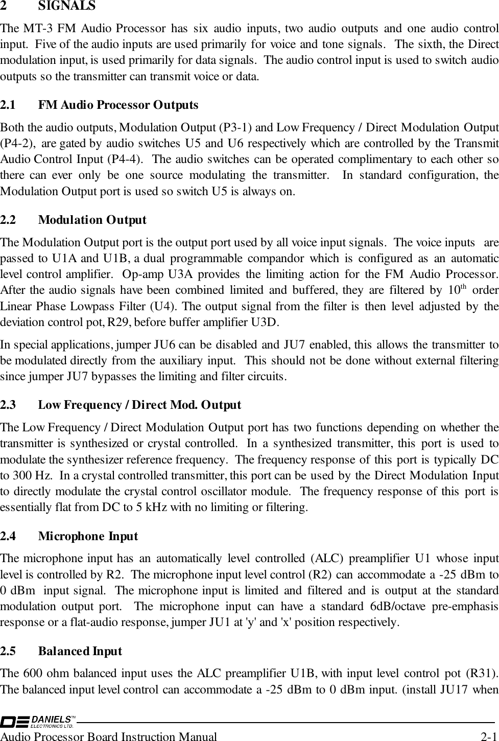
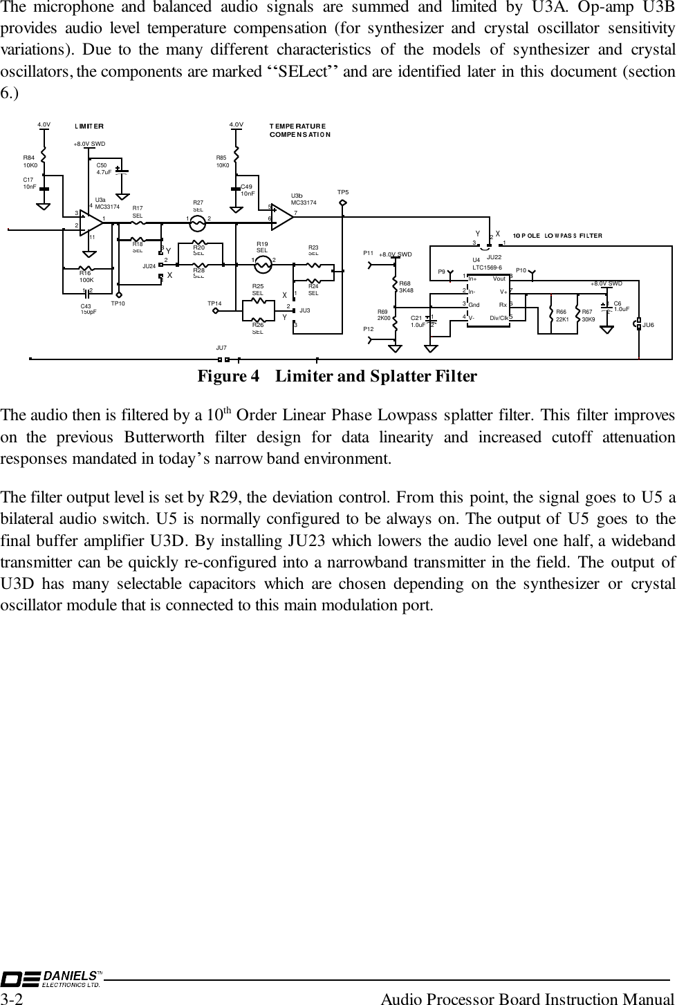
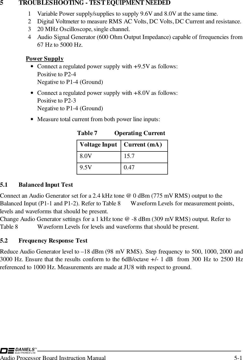
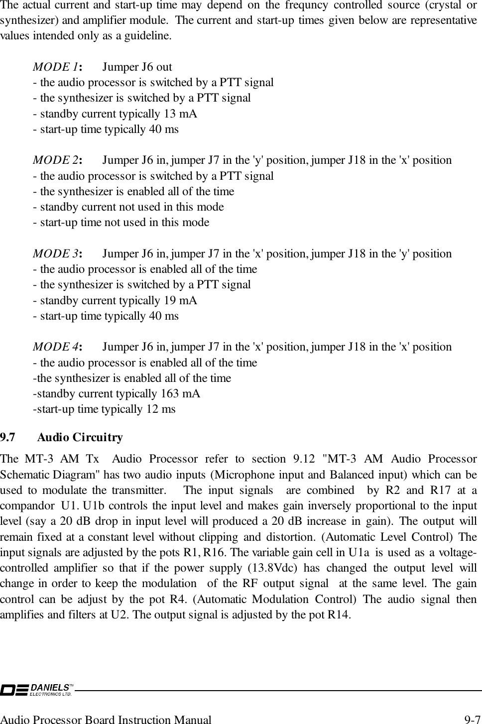
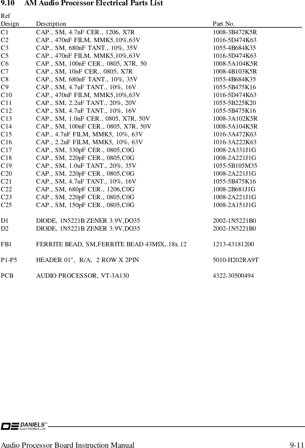
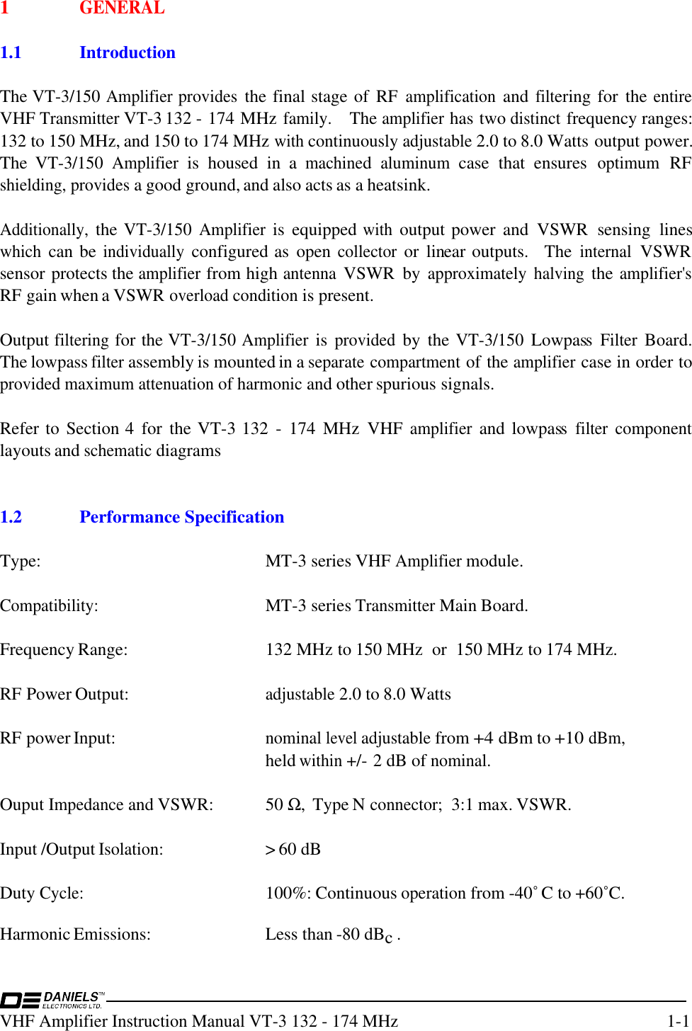
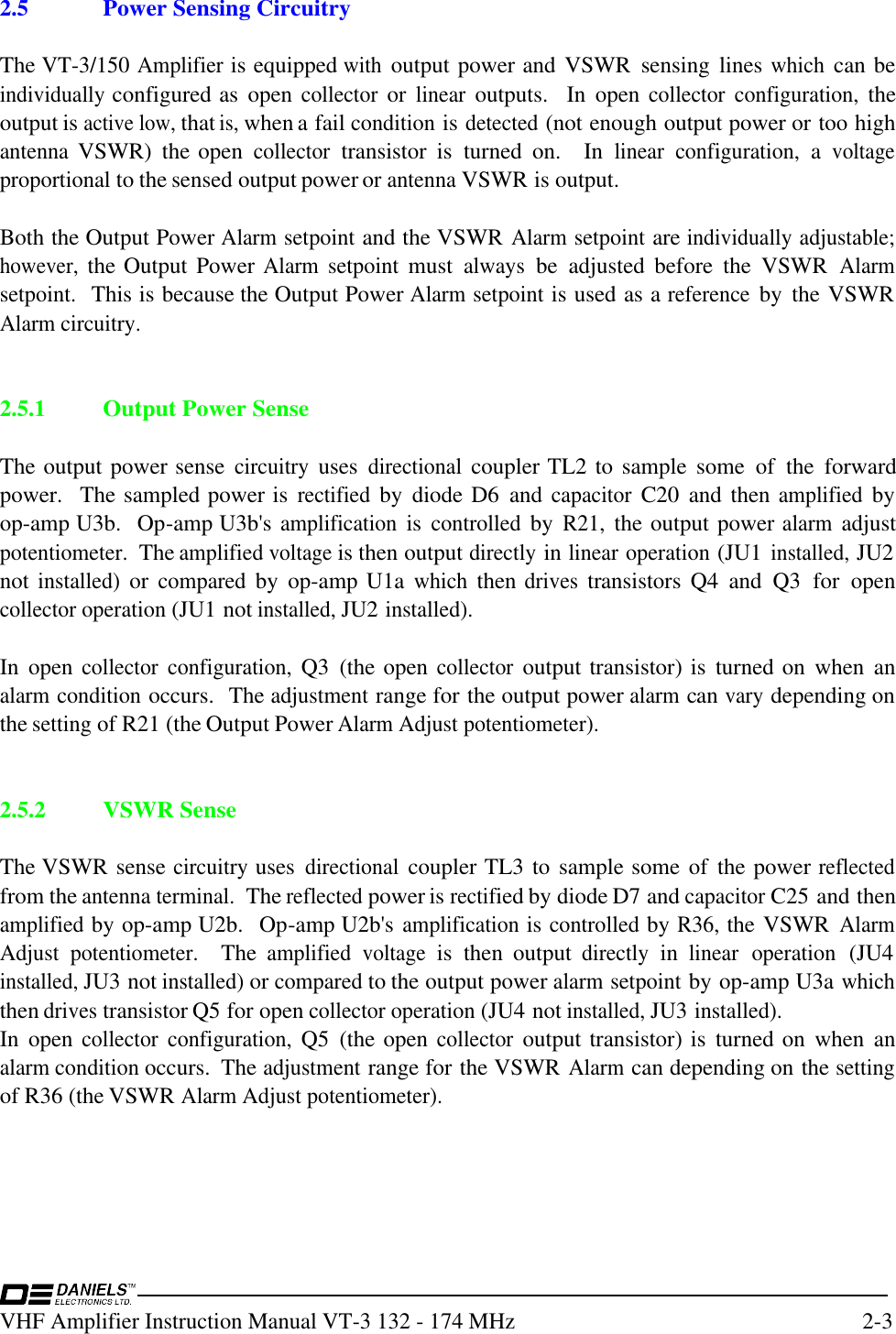
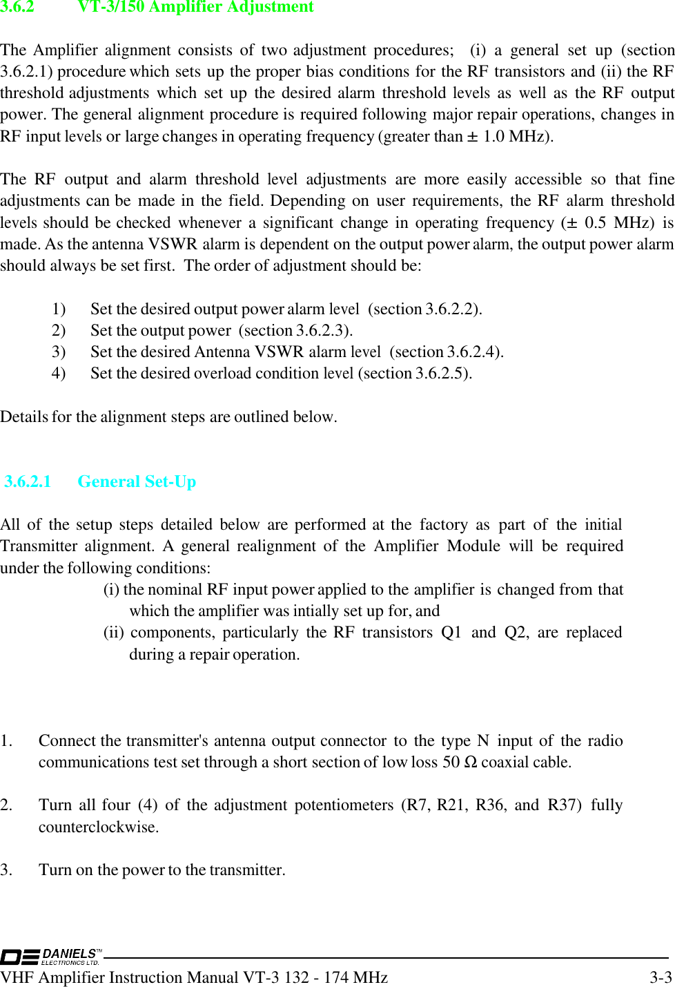
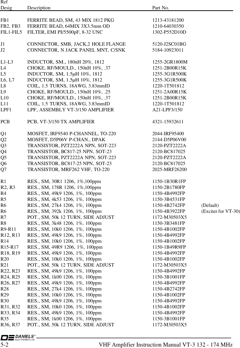
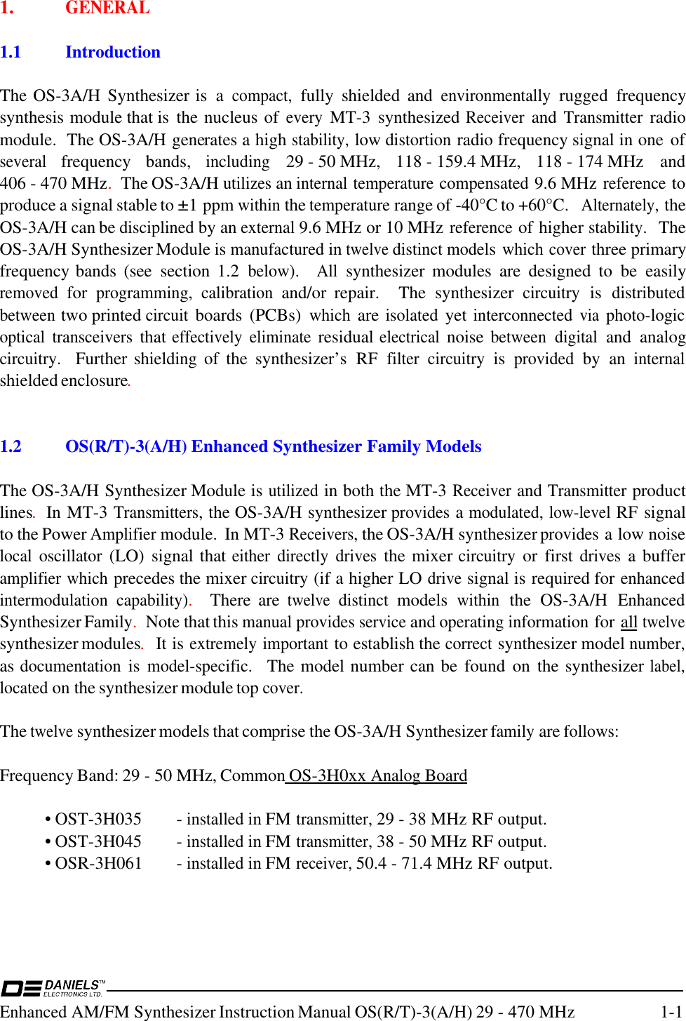
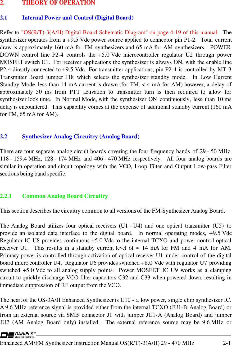
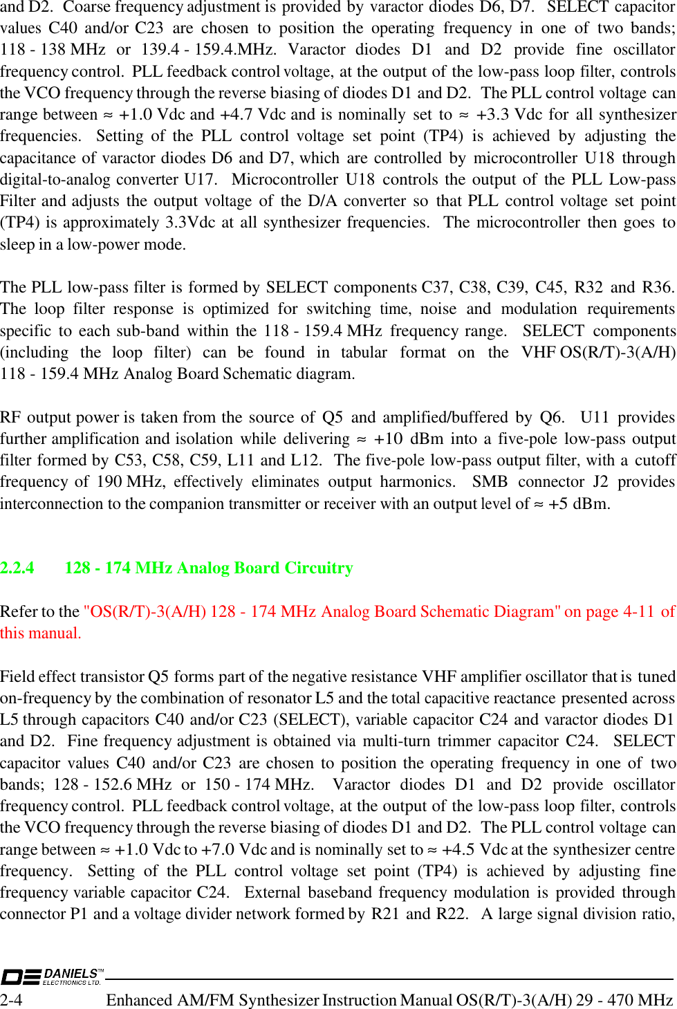
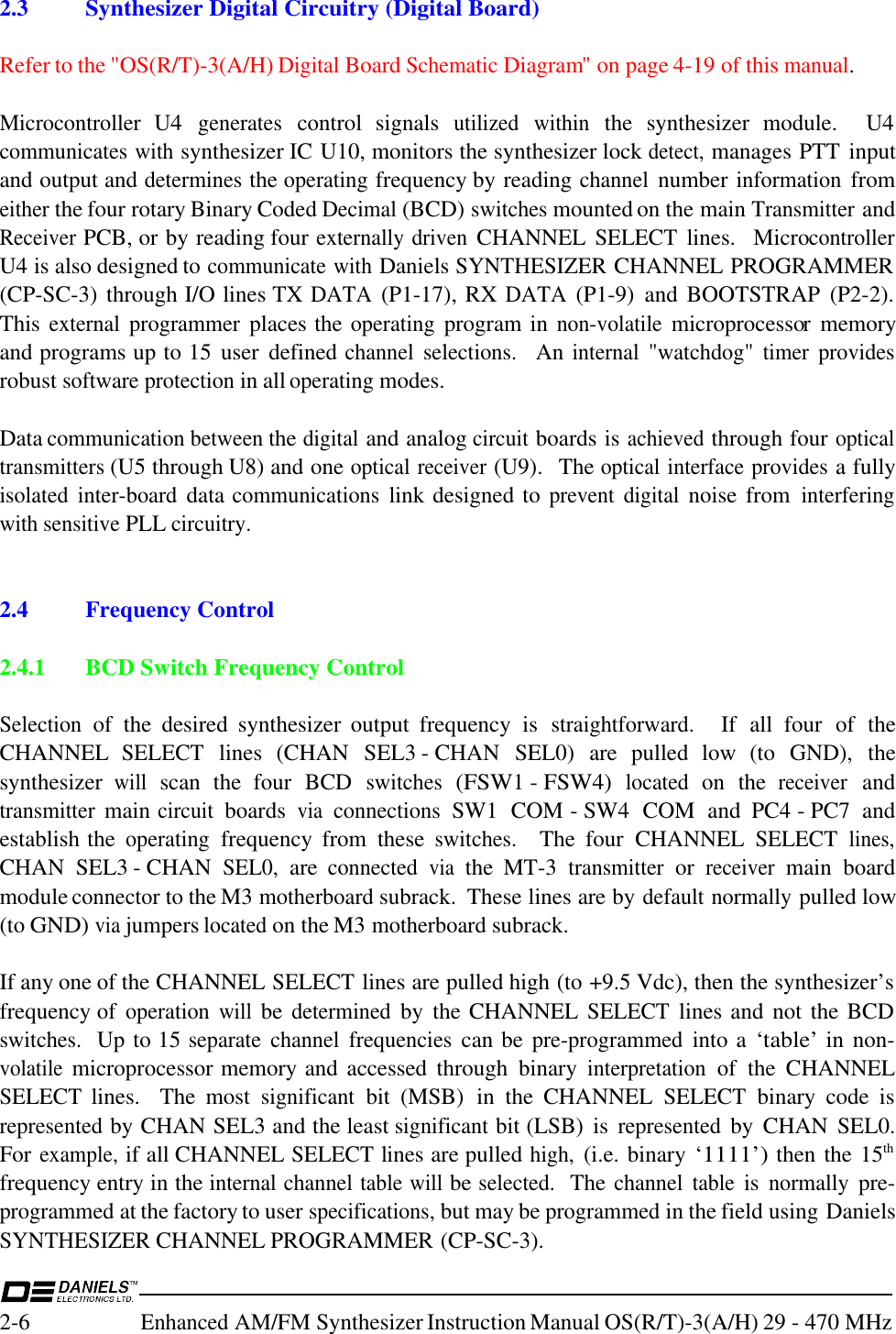
![VHF Enhanced Transmitter Instruction Manual VT-3 132 - 174 MHz2-32.2Frequency Selectioninvisible text2.2.1Synthesizer TransmitterEight backplane connections are used to communicate with the synthesizer unit. Pins D28, D30,and D32 are used (in house) to program the synthesizer. Channel select lines (pins D20, D22,D24, and D26) are used once the synthesizer is programmed to select one of 16 channels. If thechannel select lines are all low (channel 0) the frequency for the synthesizer is read from switchesFSW1 (most significant), FSW2, FSW3, and FSW4 (least significant). Refer to the VT-3/150Channel Designation Table Manual for the simplified channel number and frequency information.For all VT-3/140 models (132-150 MHz) with:• 5 kHz channel increments (BCD settings from 0000 to 4999):CHNL#= Txfrequency−128 MHz5 kHz orTxfrequency= CHNL#× 5 kHz[ ]+128 MHz• 6.25 kHz channel increments (BCD settings from 5000 to 9999):CHNL#= Txfrequency−128 MHz6.25 kHz +5000orTxfrequency= CHNL#-5000( )×6.25 kHz[ ]+128 MHzFor all VT-3/160 models (150-174 MHz) with:• 5 kHz channel increments (BCD settings from 0000 to 4999):CHNL#= Txfrequency−150 MHz5 kHz orTxfrequency= CHNL#× 5 kHz[ ]+150 MHz• 6.25 kHz channel increments (BCD settings from 5000 to 9999):CHNL#= Txfrequency−150 MHz6.25 kHz +5000orTxfrequency= CHNL#-5000( )×6.25kHz[ ]+150 MHz](https://usermanual.wiki/Codan-Radio-Communications/VT-3-150-SN/User-Guide-134541-Page-12.png)
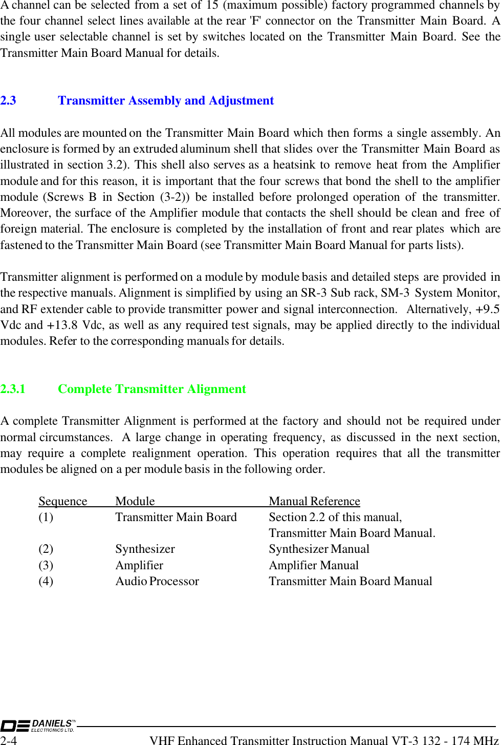
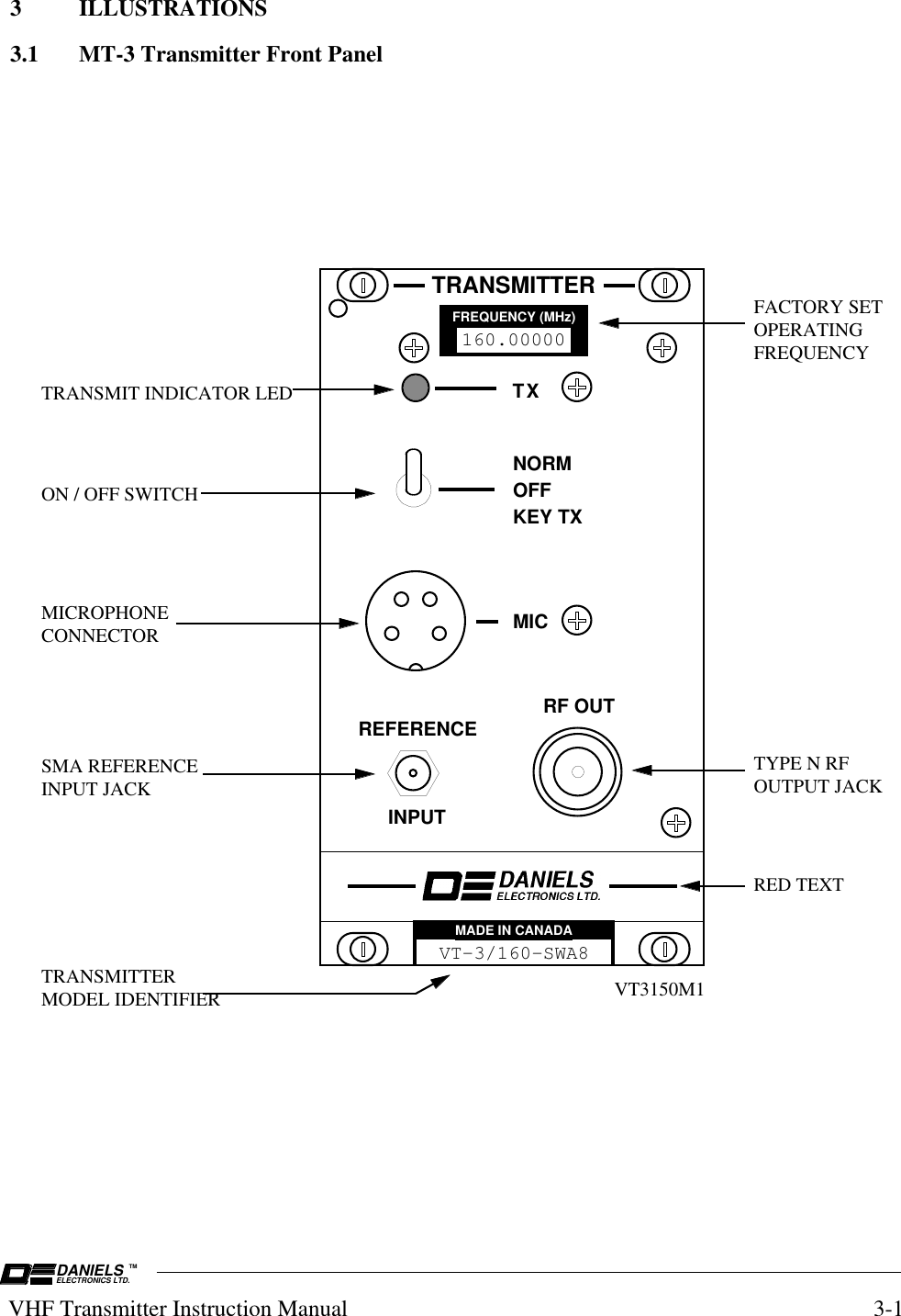
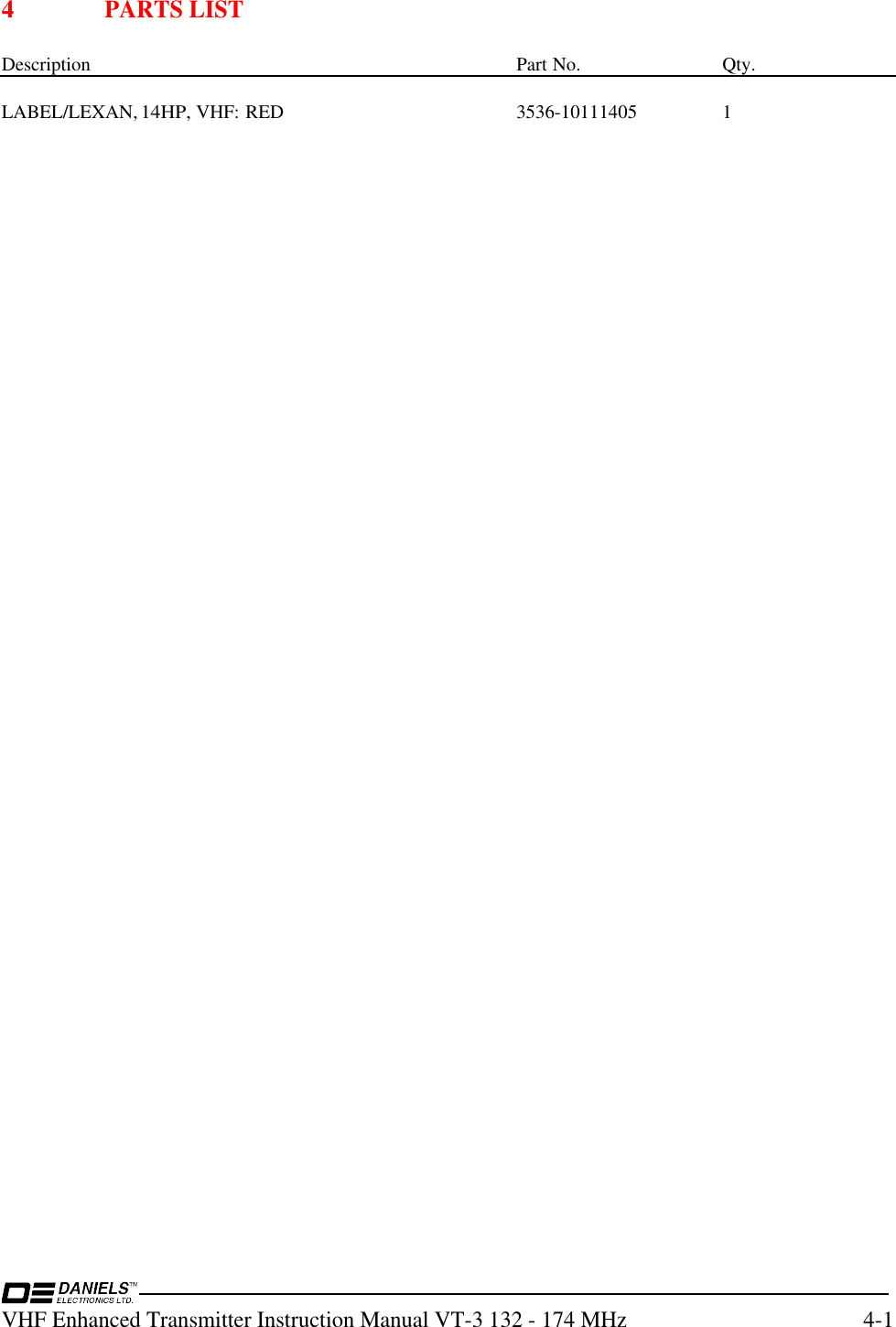

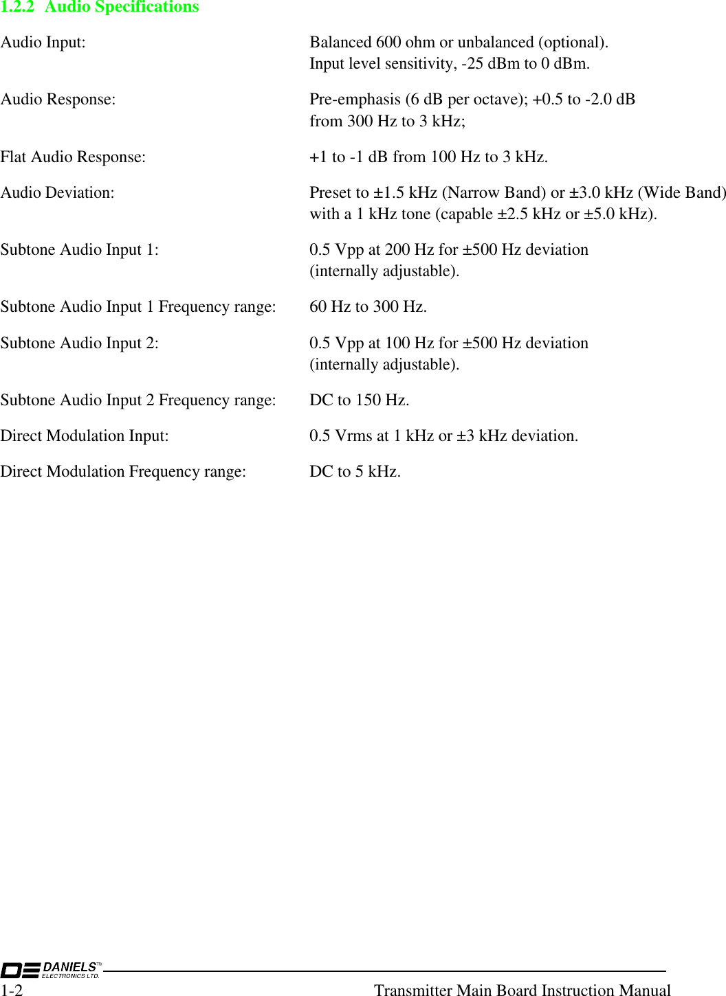
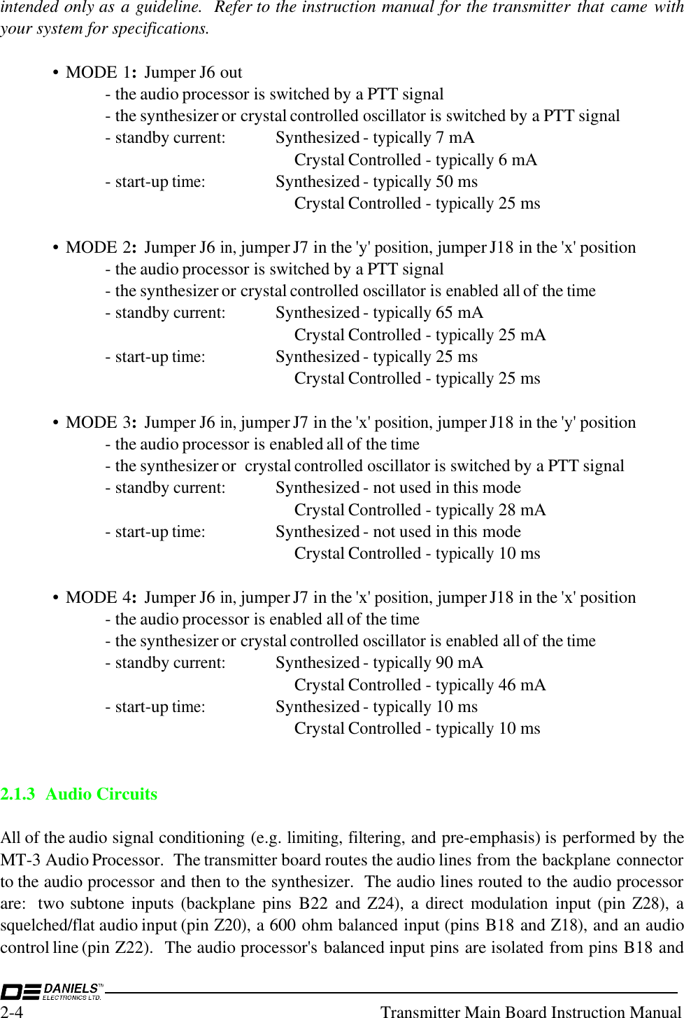
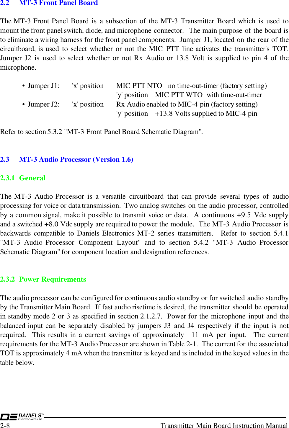
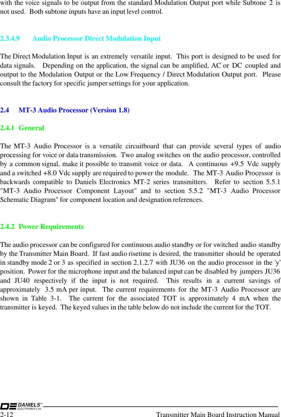
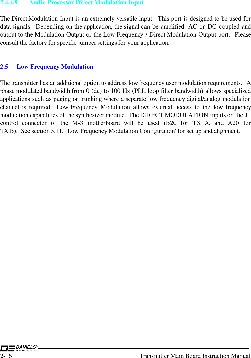
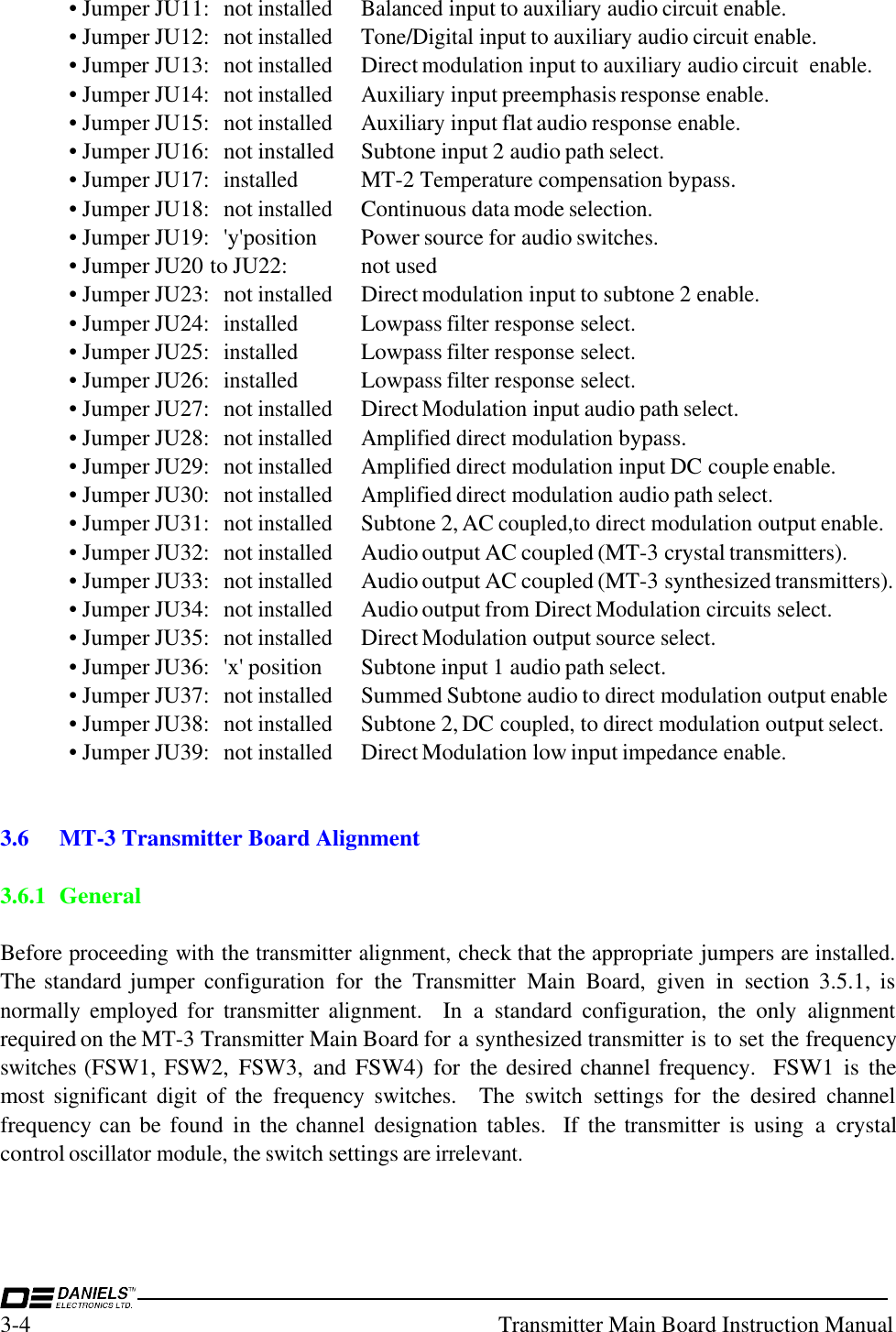
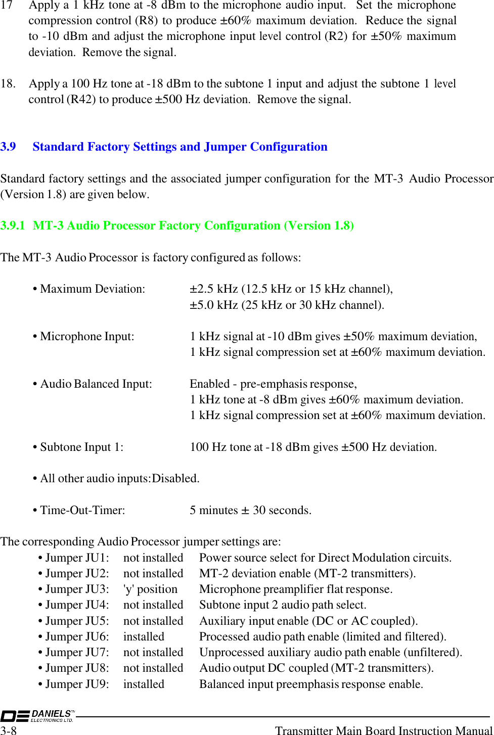

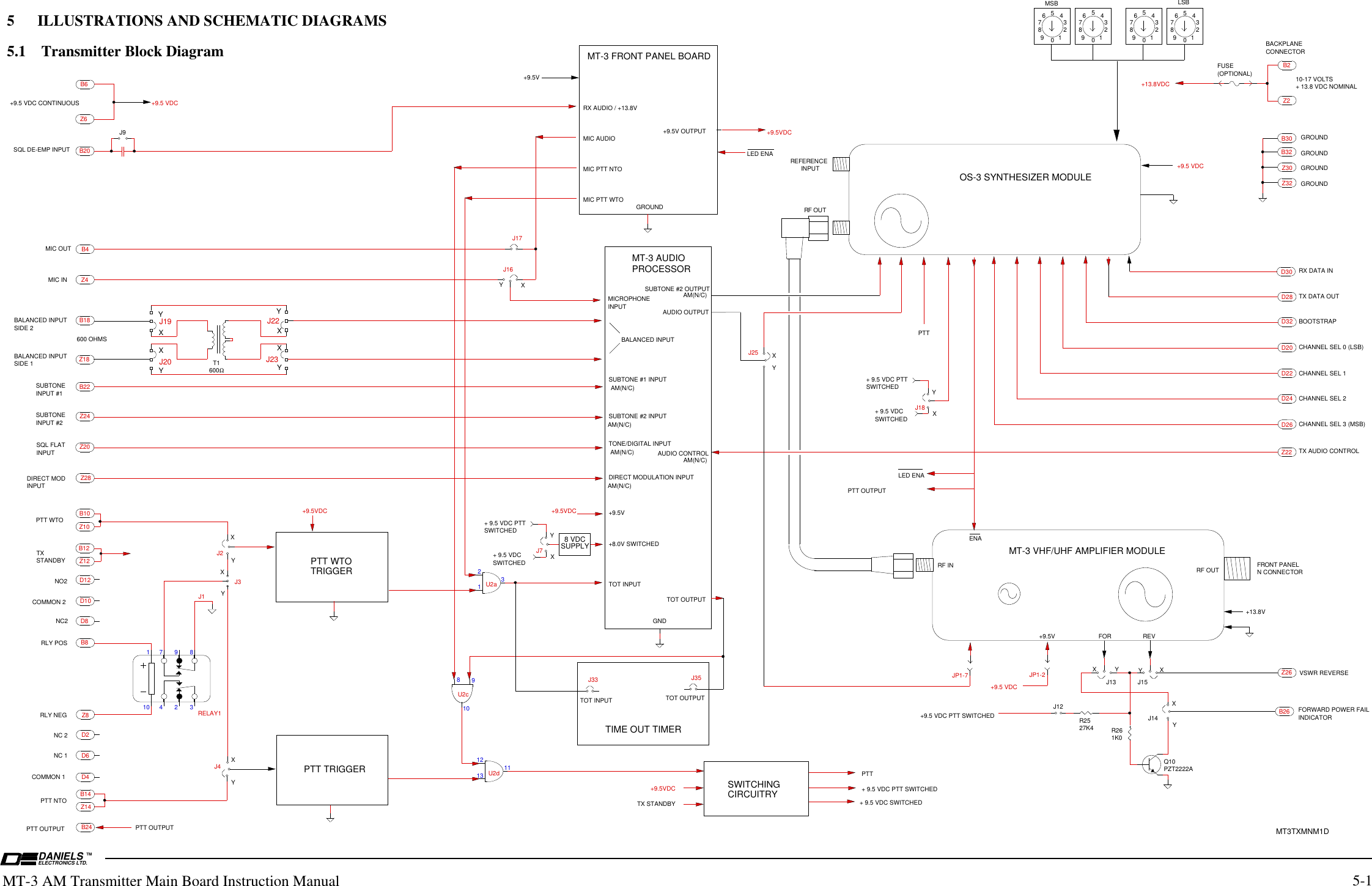
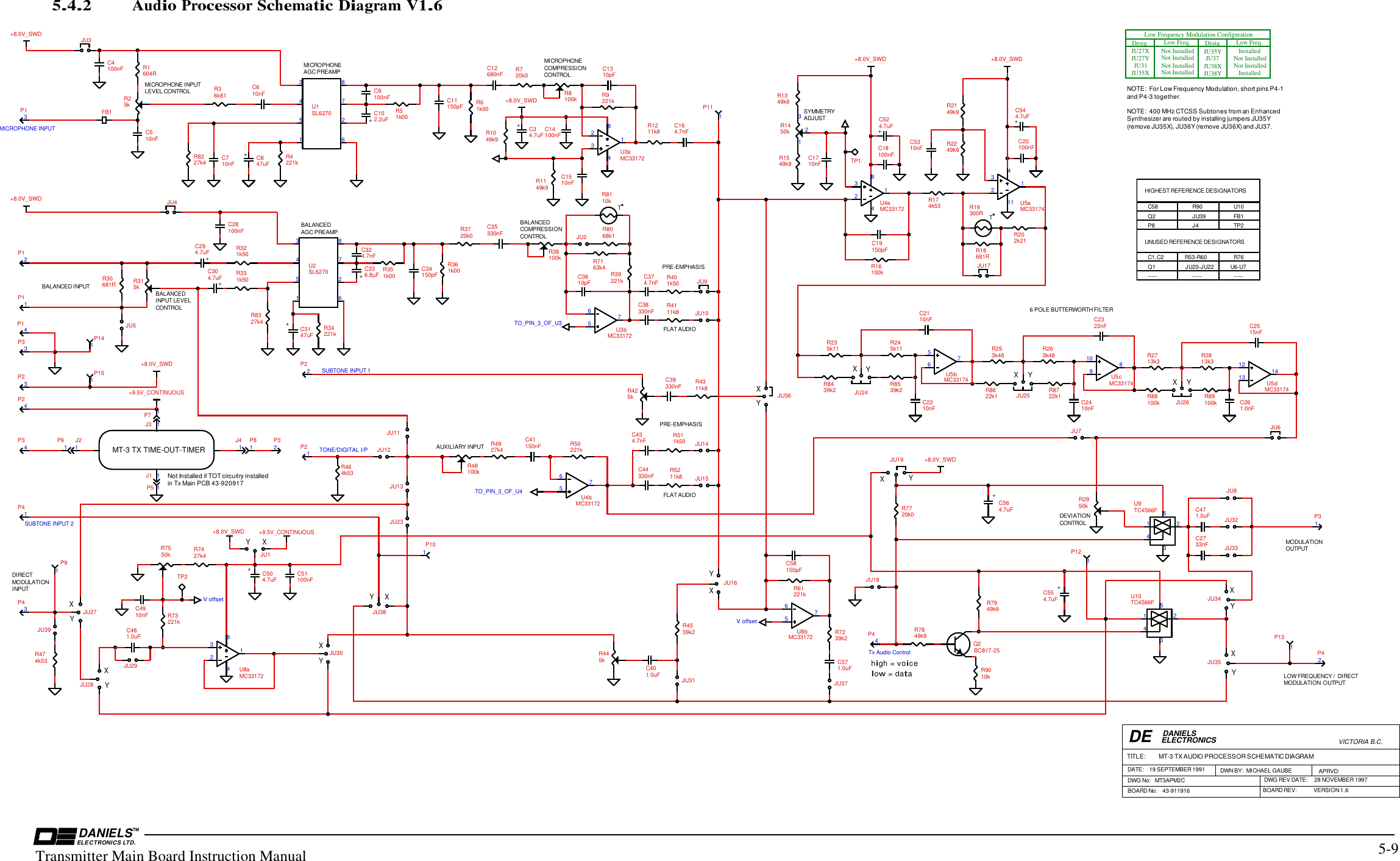

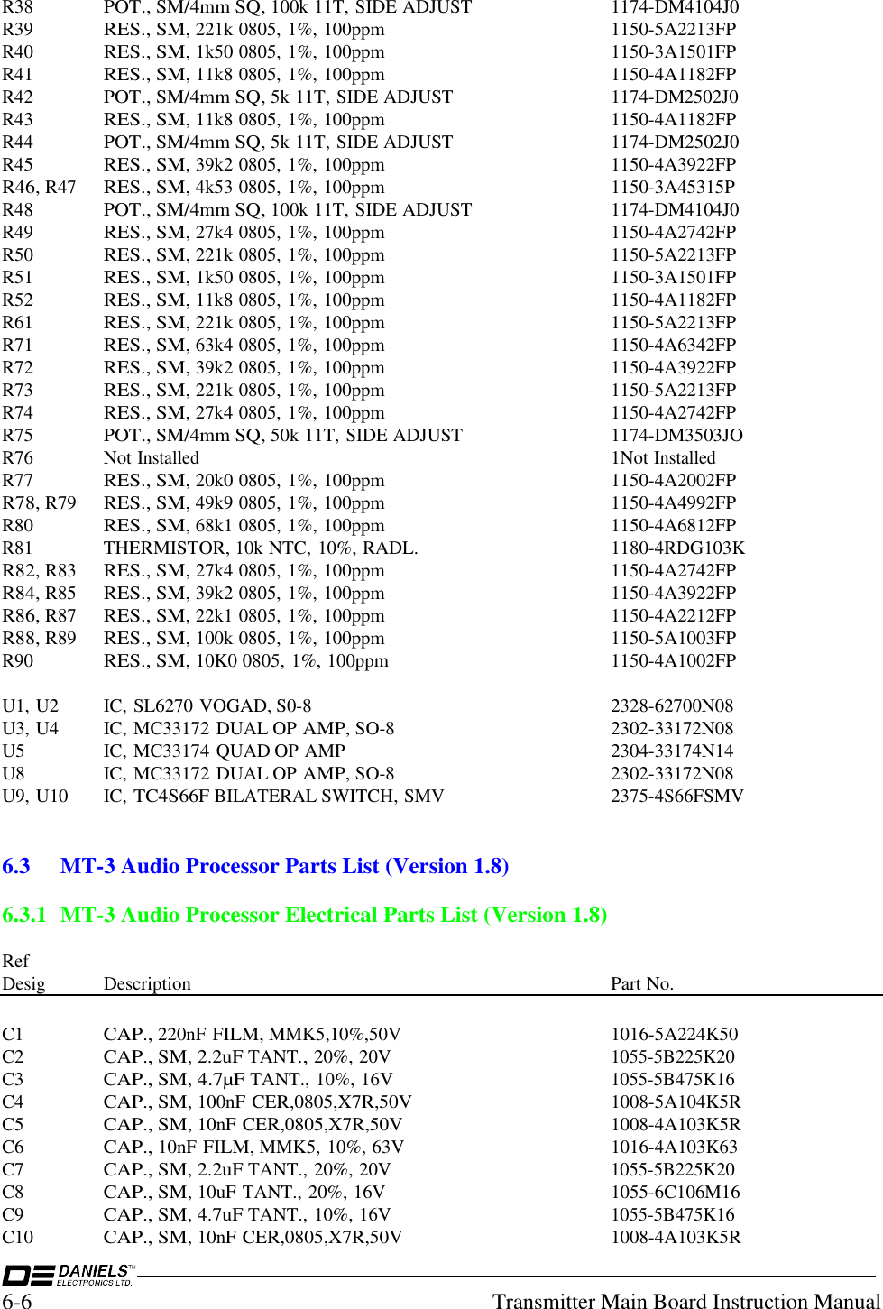
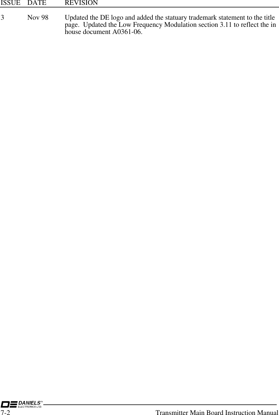
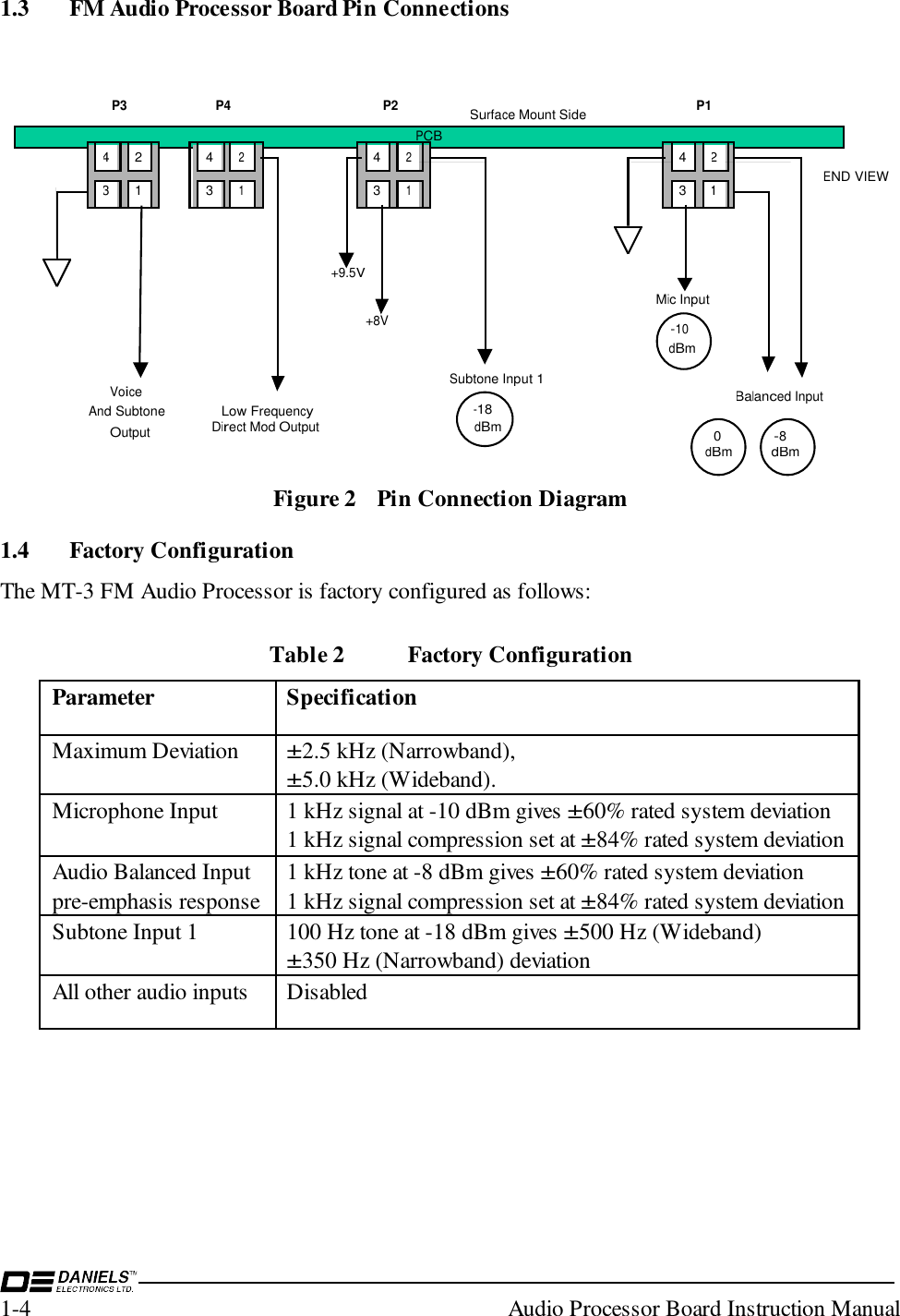
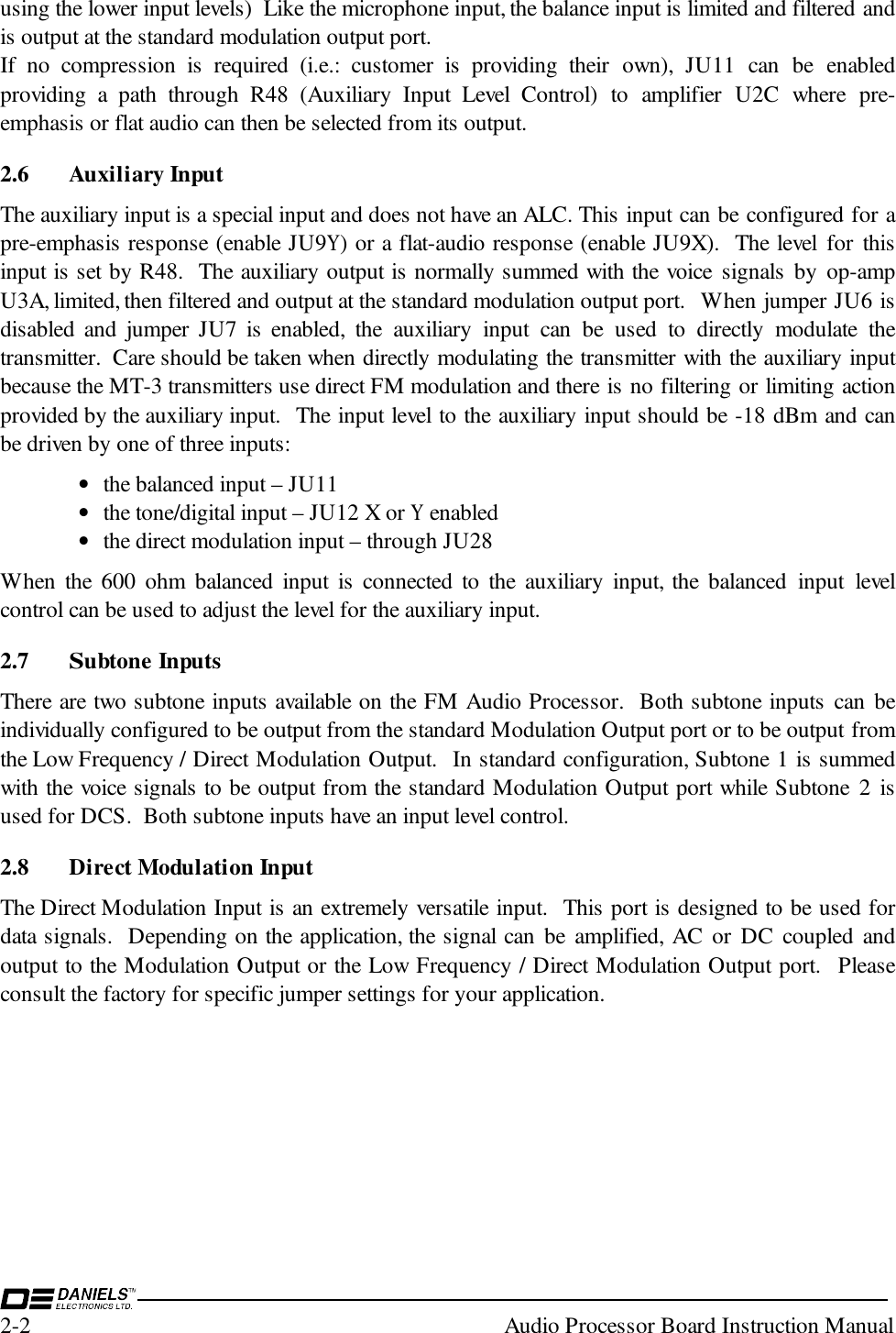
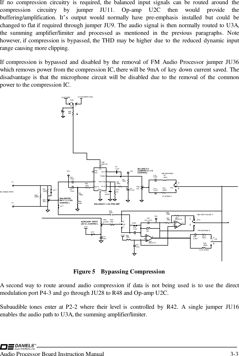
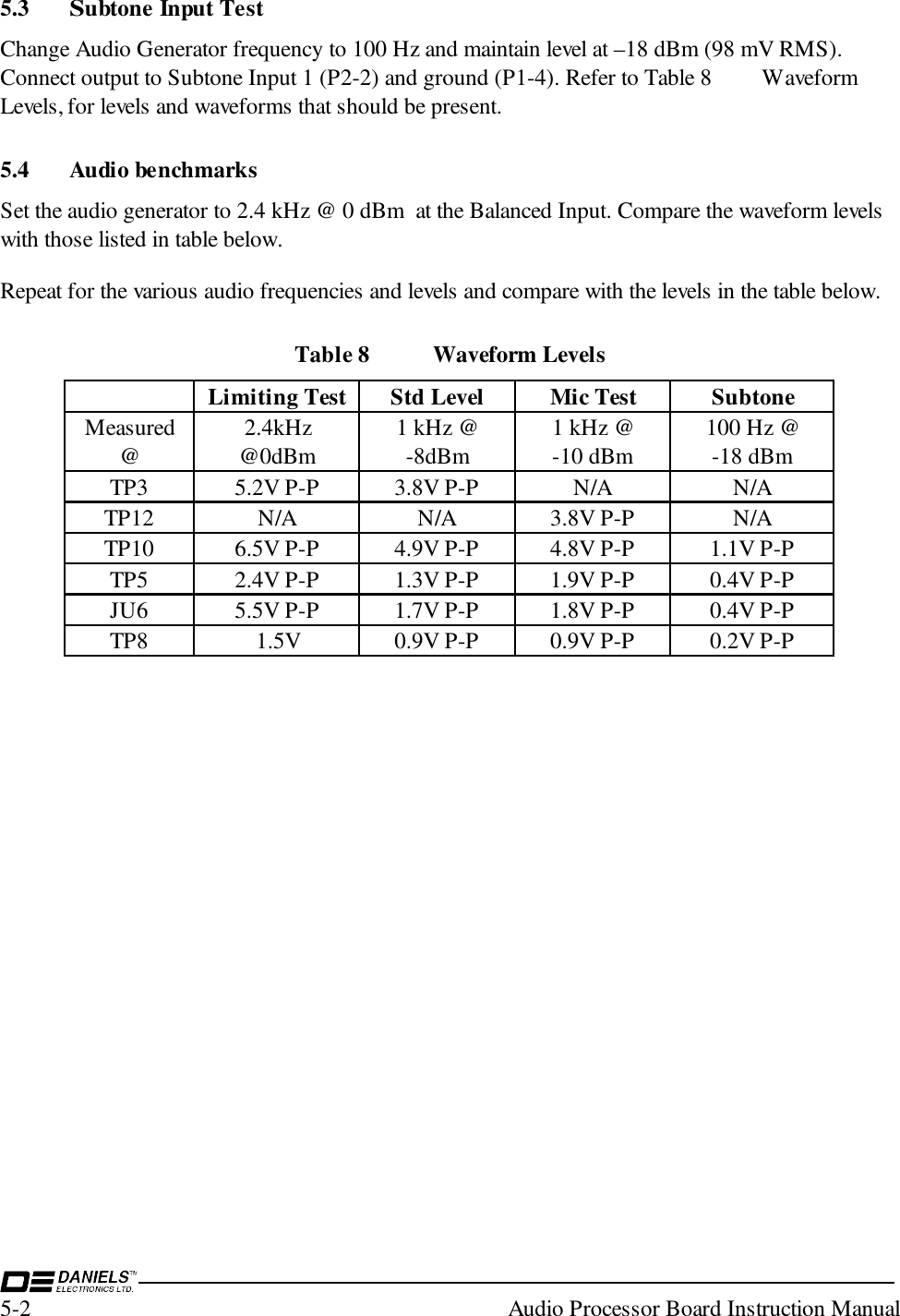


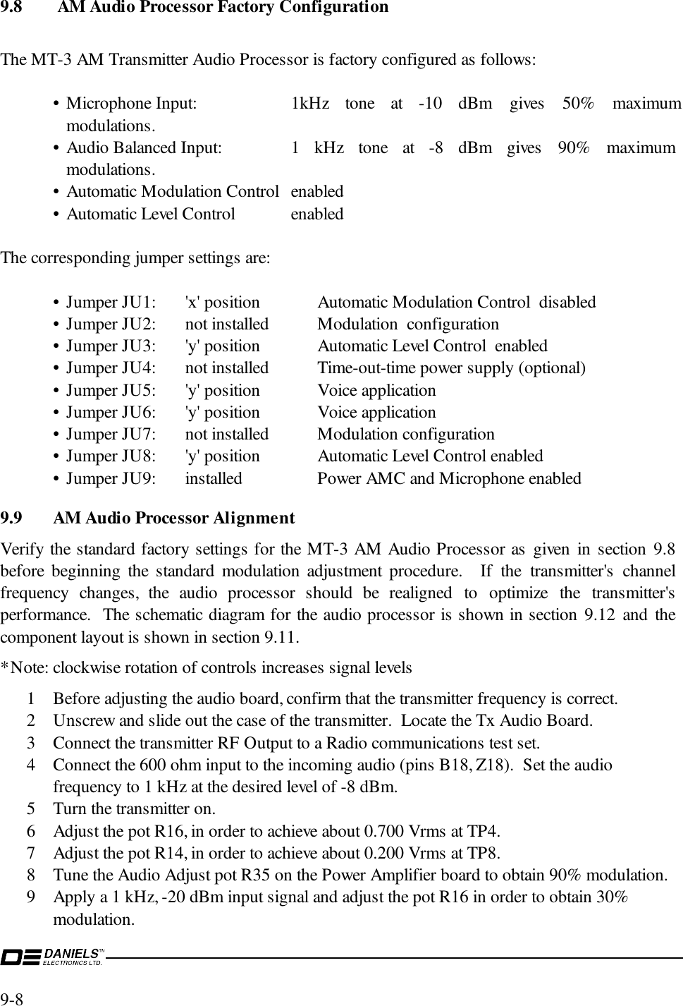
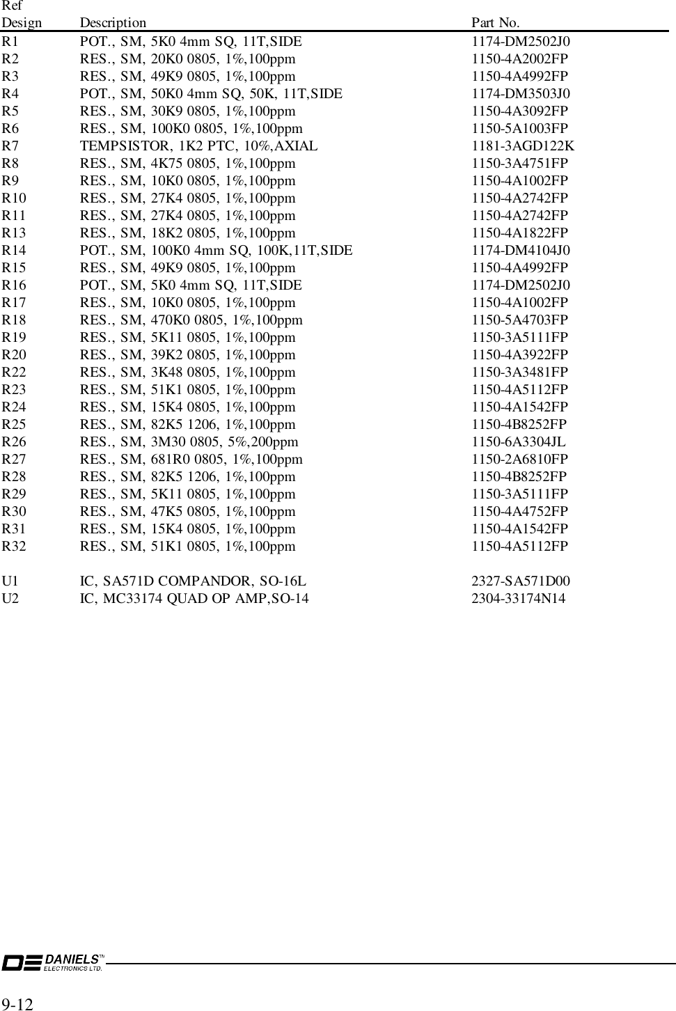


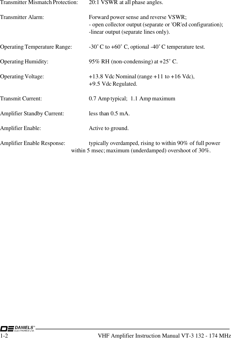
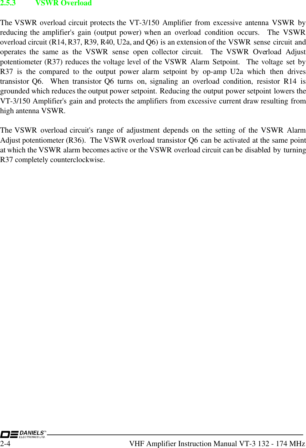
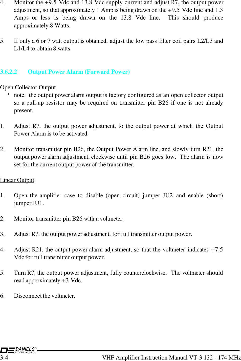
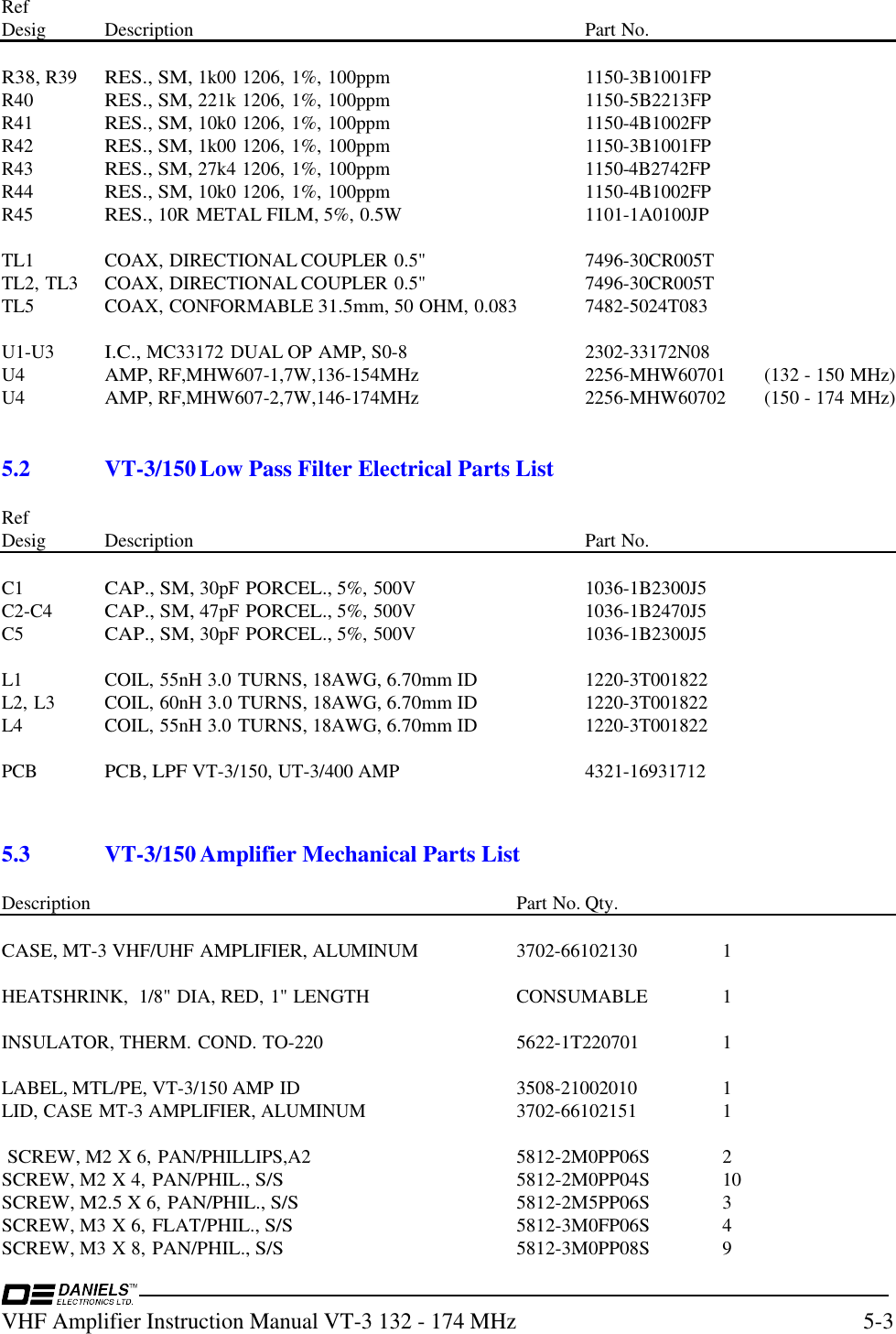
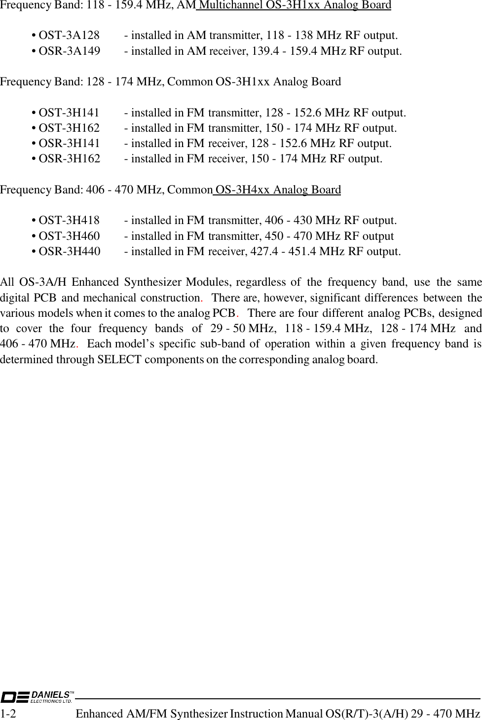
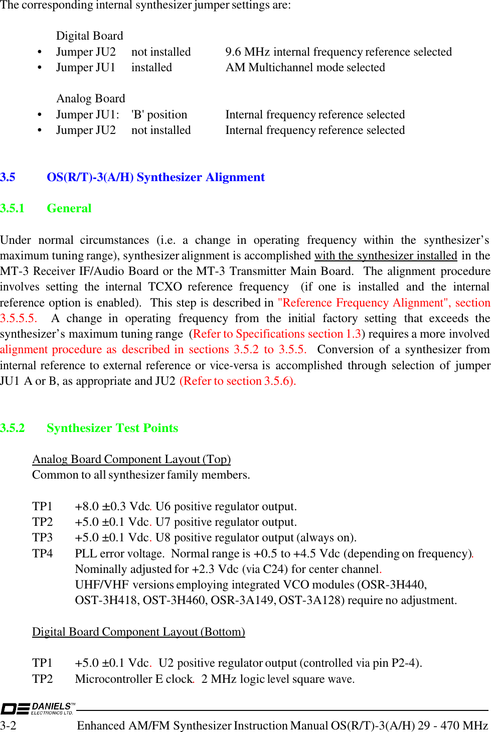
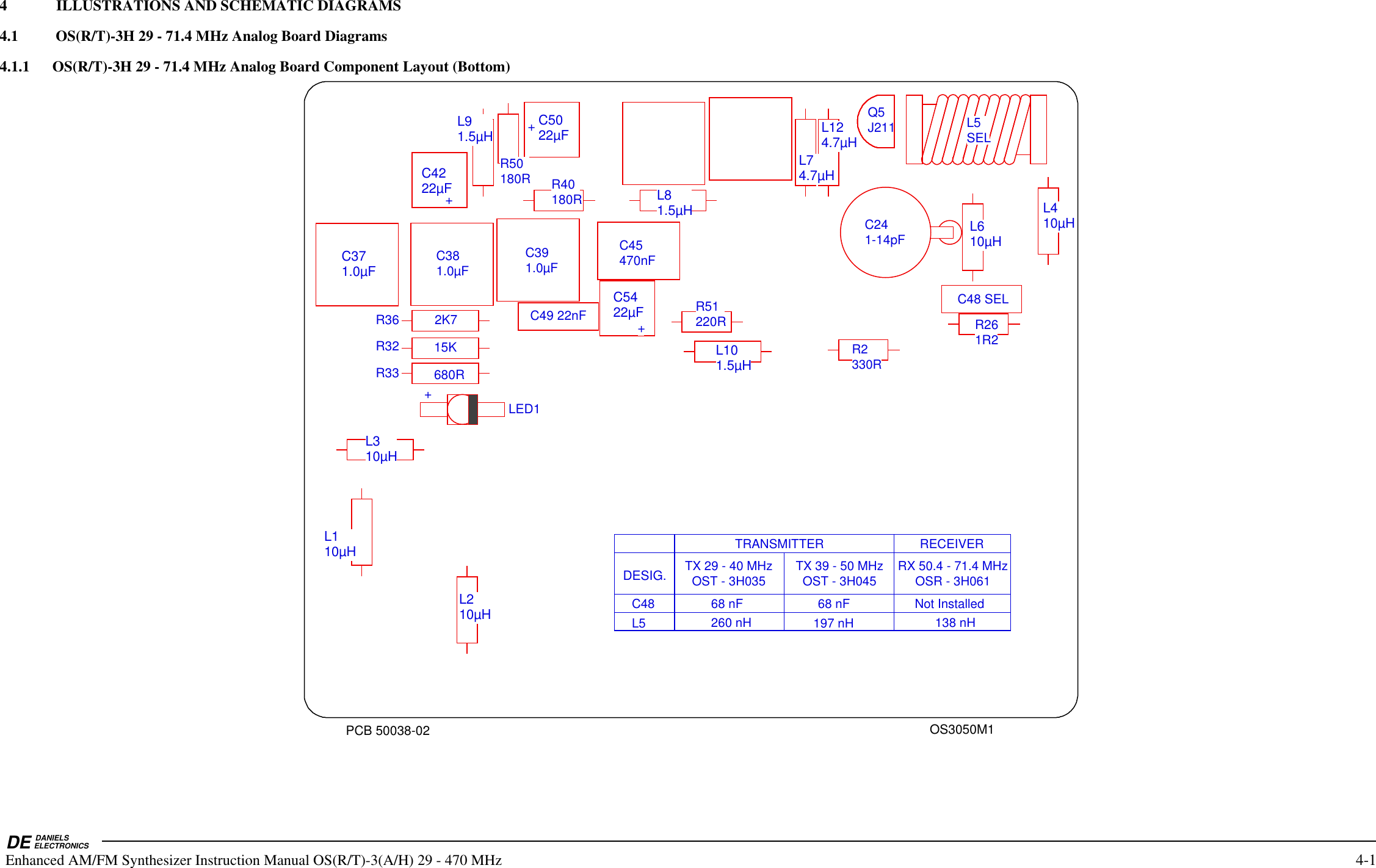
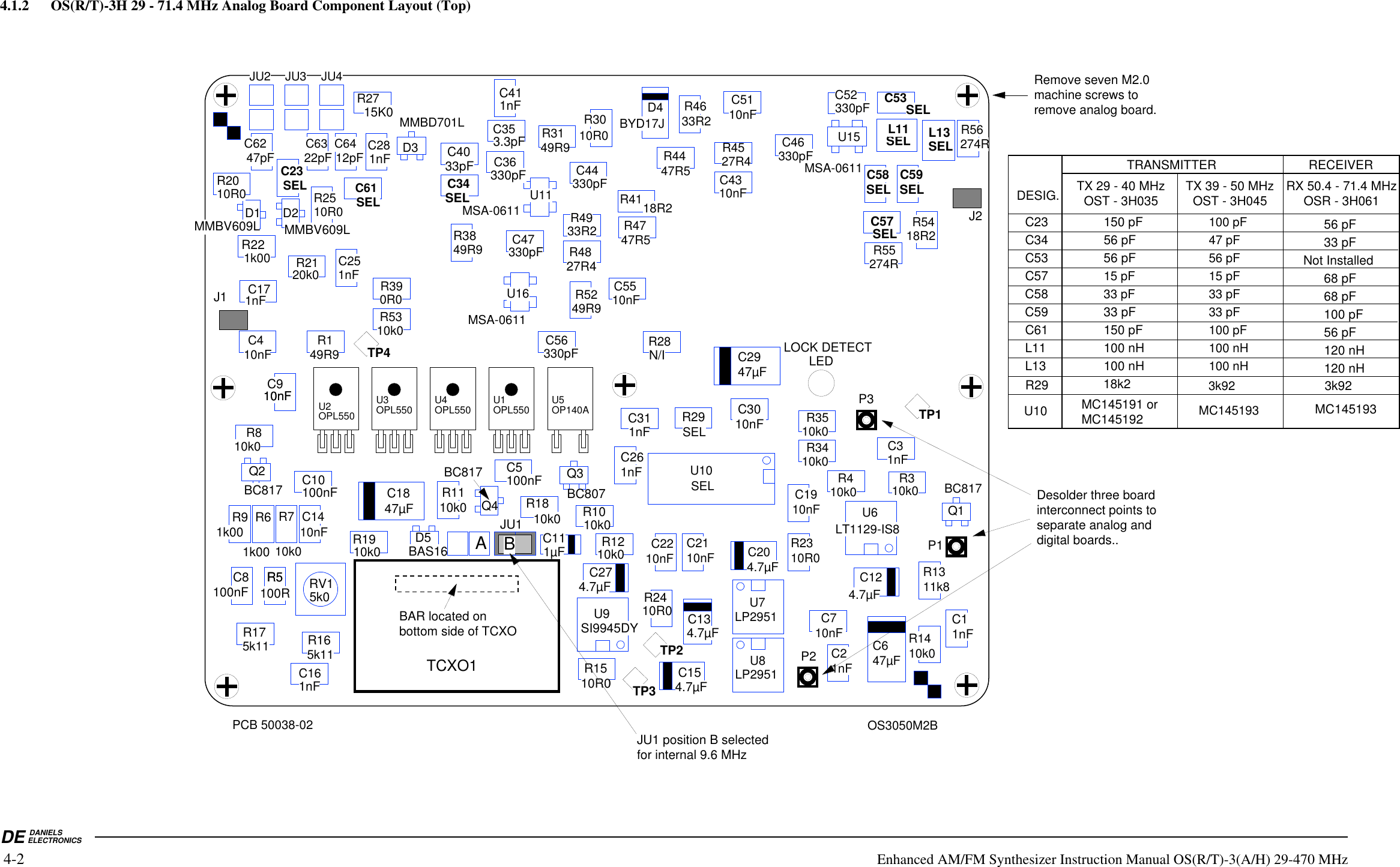
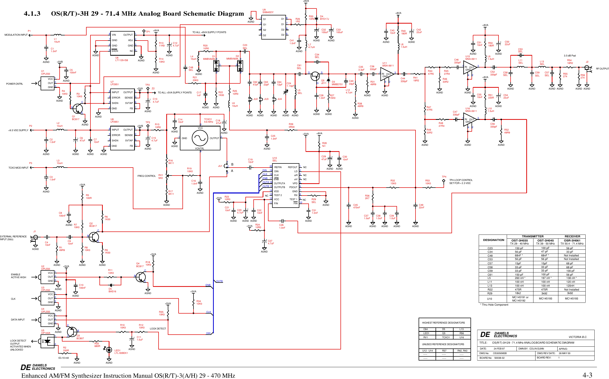
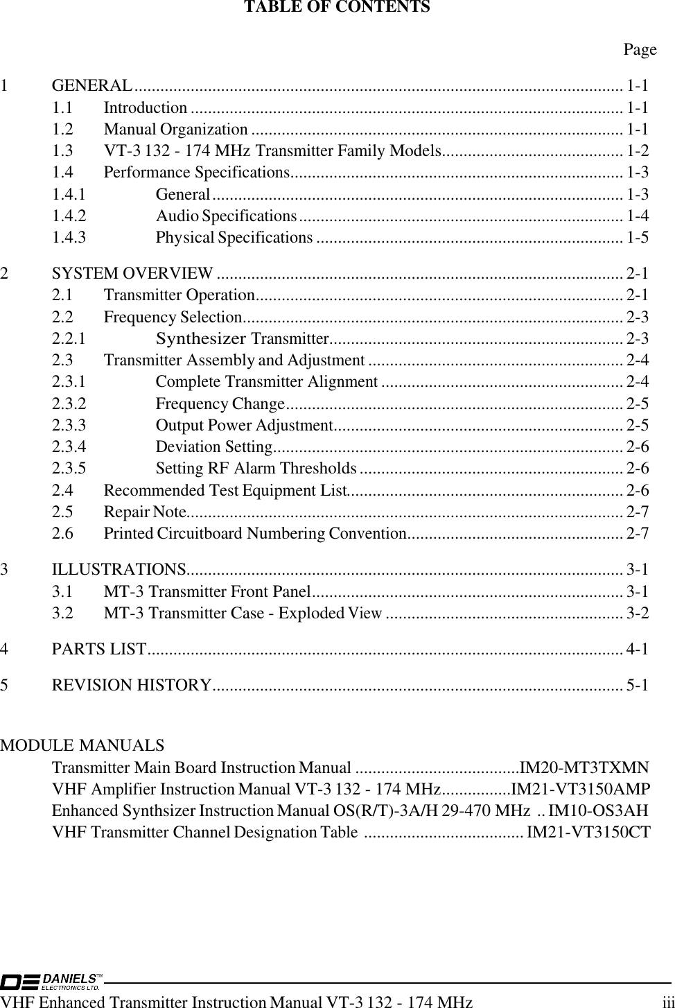
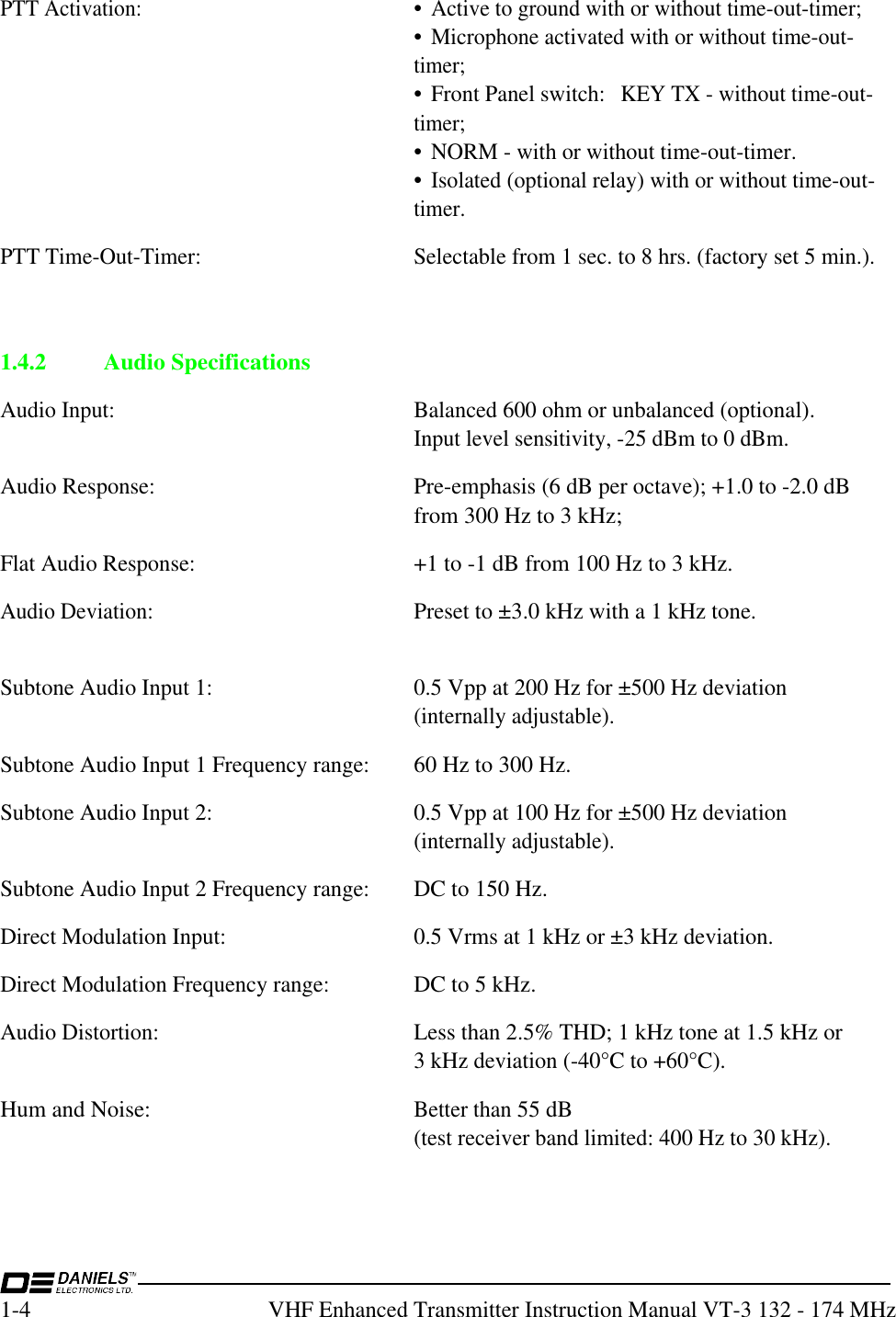
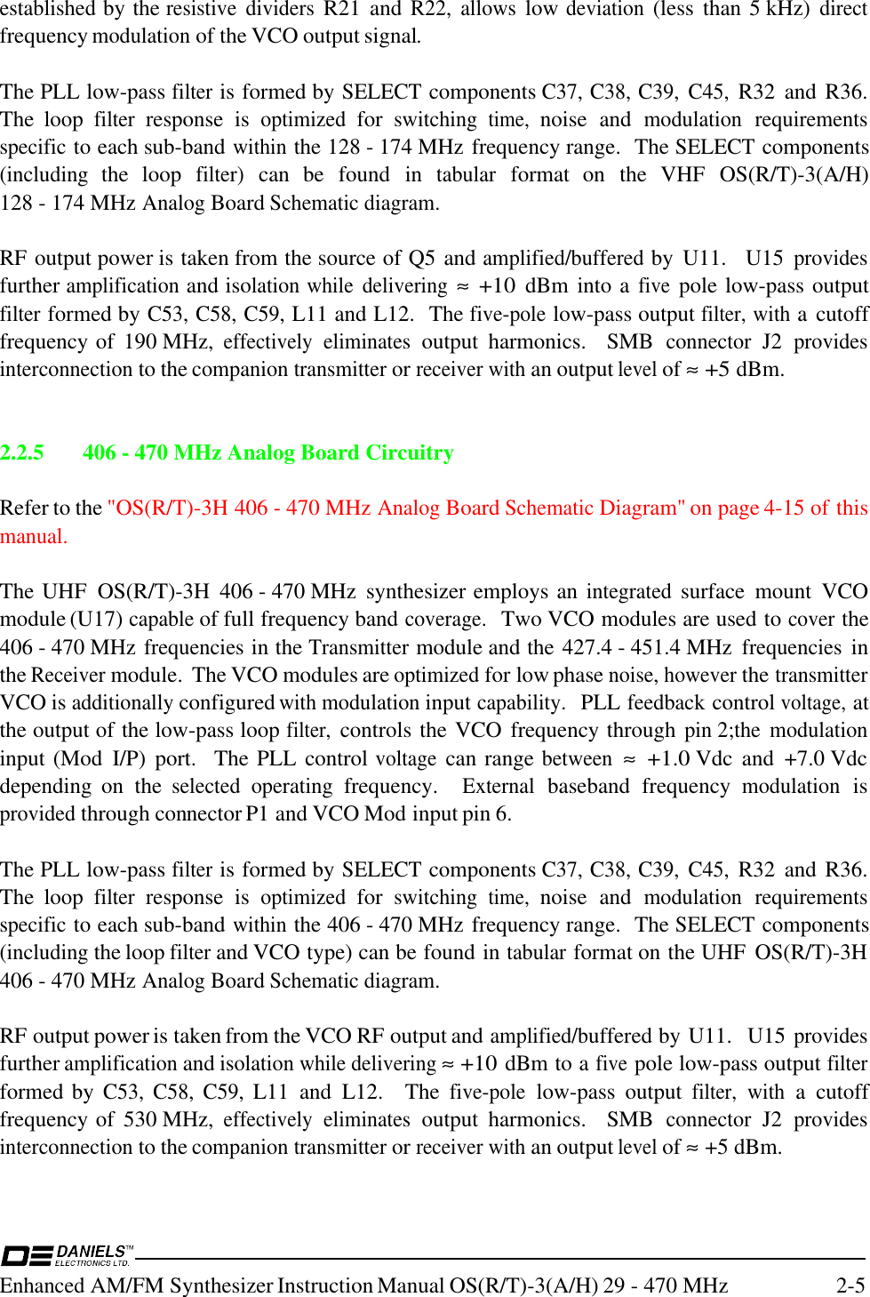
![Enhanced AM/FM Synthesizer Instruction Manual OS(R/T)-3(A/H) 29 - 470 MHz 1-31.3 Performance SpecificationsType:Narrow band FM, Single loop synthesizer module utilizing low noise VCO and PLL technology.Compatible with Daniels MT-3 series Transmitter and Receiver modules.Frequency Range:29 MHz - 38 MHz [±0.5 MHz] (OST-3H035)(Tuning range with no adjustment 38 MHz - 50 MHz [±1.0 MHz] (OST-3H045)is shown in [ ] brackets.) 50.4 MHz - 71.4 MHz [±1.0 MHz] (OSR-3H061)118 MHz -138 MHz [Full band] (OST-3A128)128 MHz - 152.6 MHz [±2.0 MHz] (OST-3H141, OSR-3H141)139.4 MHz - 159.4 MHz [Full band] (OSR-3A149)150 MHz - 174 MHz [±2.0 MHz] (OST-3H162, OSR-3H162)406 MHz - 430 MHz [Full band] (OST-3H418)427.4 MHz - 451.4 MHz [Full band] (OSR-3H440)450 MHz - 470 MHz [Full band] (OST-3H460)Output Power:+5 dBm ±2 dBm into 50ΩHarmonics:<-30 dBcSpurious:<-90 dBc<-70 dBc above 400 MHzAttack Time:<10 ms (Normal Mode)<50 ms (Low Current Standby Mode)Hum and Noise: -55 dB](https://usermanual.wiki/Codan-Radio-Communications/VT-3-150-SN/User-Guide-134541-Page-165.png)
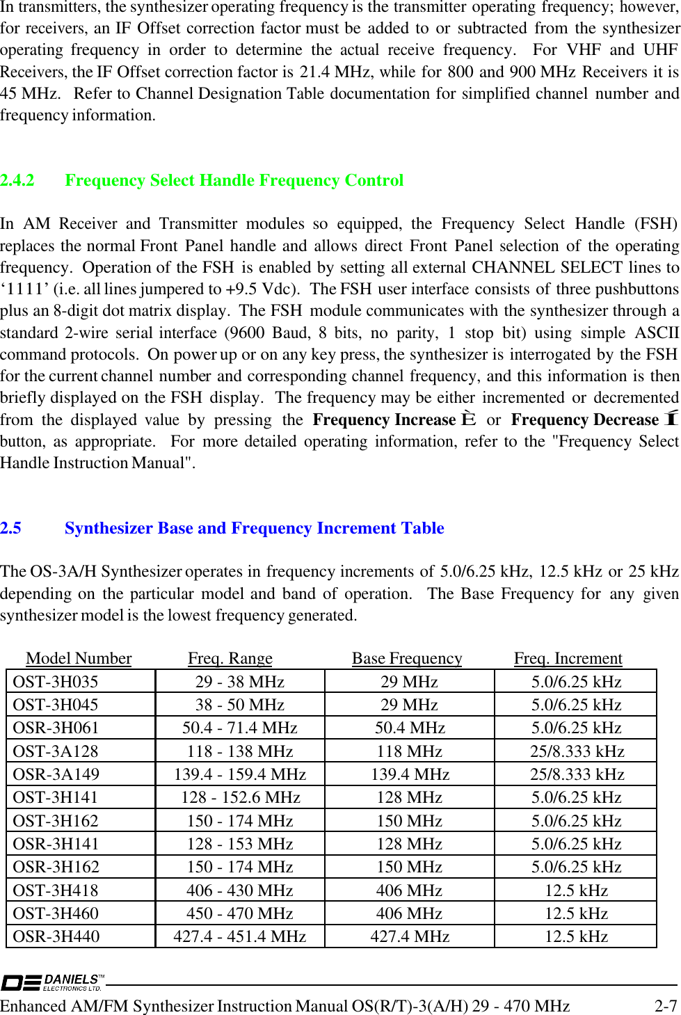
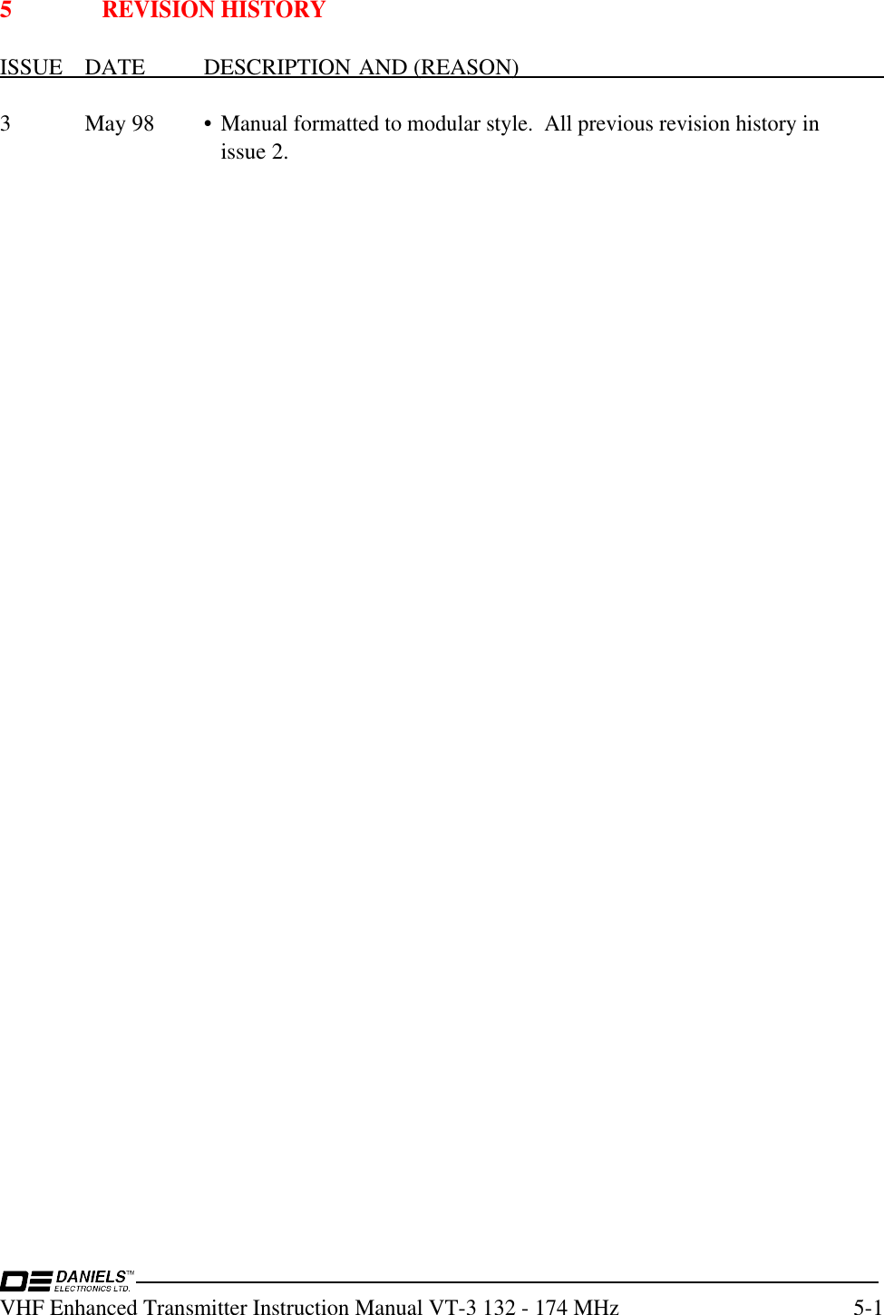
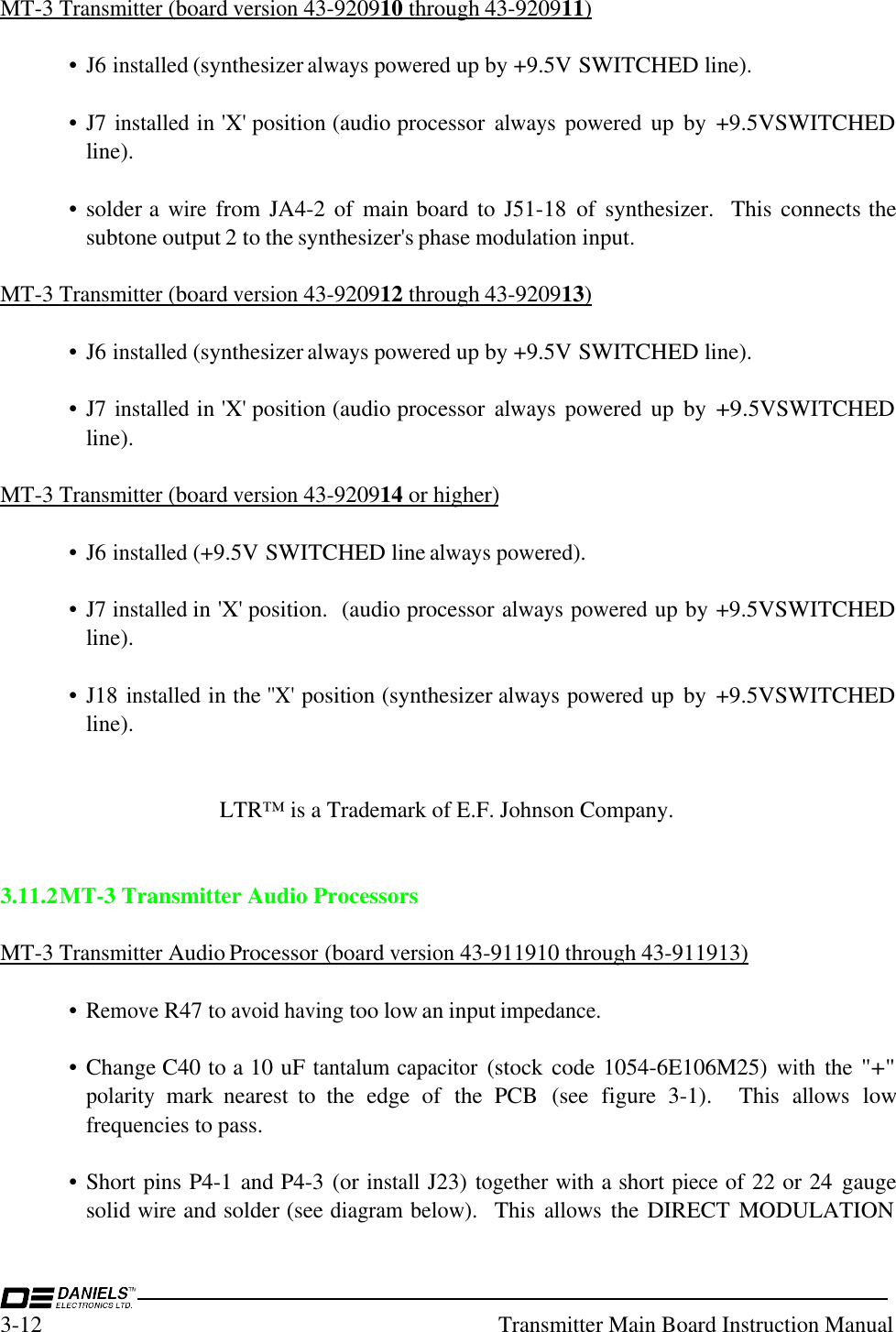
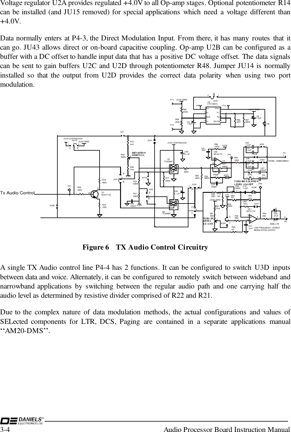
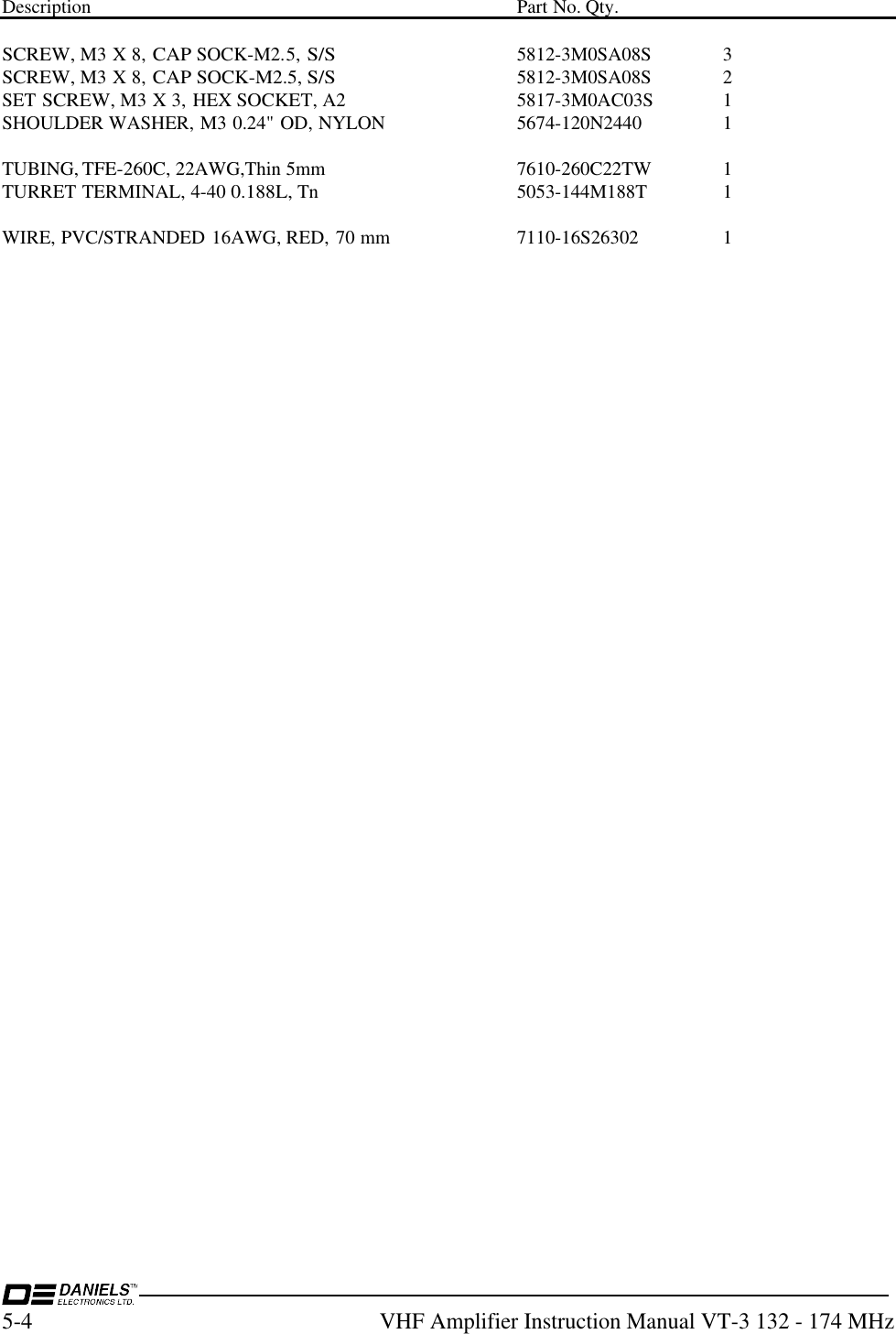
![2-8Enhanced AM/FM Synthesizer Instruction Manual OS(R/T)-3(A/H) 29 - 470 MHz2.6 5.0/6.25 kHz Channelization.All Daniels VHF synthesizers (excluding AM synthesizers) have been designed to generatefrequencies in both 5.0 kHz and 6.25 kHz channel increments. BCD channel switch settings from0000 to 4999 will therefore select operating frequencies with 5.0 kHz increments, while BCDswitch settings from 5000 to 9999 will select operating frequencies with 6.25 kHz increments.Calculation of the operating frequency for VHF synthesizers capable of 5.0/6.25 kHzchannelization is determined as follows:•BCD switch settings from 0000 to 4999: Multiply the switch setting by 5.0 kHz and addthe result to the synthesizer base frequency.Example: An OST-3H141 synthesizer has a base frequency of 128 MHz. Theselected channel number is 0988. The synthesizer output frequency is:((988 x 5 kHz) + 128 MHz) = 132.940 MHz•BCD switch settings from 5000 to 9999: Subtract 5000 from the switch setting. Multiplythe result by 6.25 kHz and add the result to the synthesizer base frequency.Example: An OSR-3H162 synthesizer has a base frequency of 150 MHz. Theselected channel number is 7205. The synthesizer output frequency is:((7205-5000) x 6.25 kHz) + 150 MHz) = 163.78125 MHz2.7 8.333 kHz Channelization.Daniels AM synthesizers have been designed to generate frequencies in 8.333 kHz increments. InNorth America, AM channels and operating frequencies are allocated in triples of 8.333 kHz(i.e. 25 kHz steps). The operating frequency for synthesizers having 8.333 kHz channelization isdetermined as follows:•Multiply the BCD switch setting by 8.333 kHz and add the result to the synthesizer basefrequency.Example: An OST-3A128 synthesizer has a base frequency of 118 MHz. Theselected channel number is 0231. The synthesizer output frequency is:[(1200 x 8.333 kHz) + 118 MHz] = 128.000 MHz](https://usermanual.wiki/Codan-Radio-Communications/VT-3-150-SN/User-Guide-134541-Page-176.png)