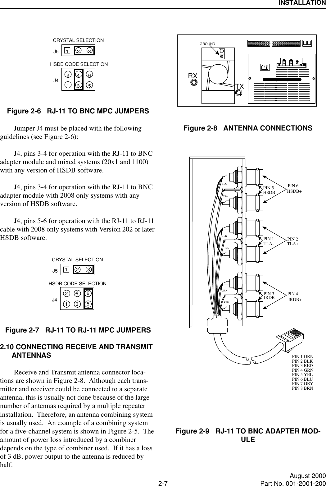
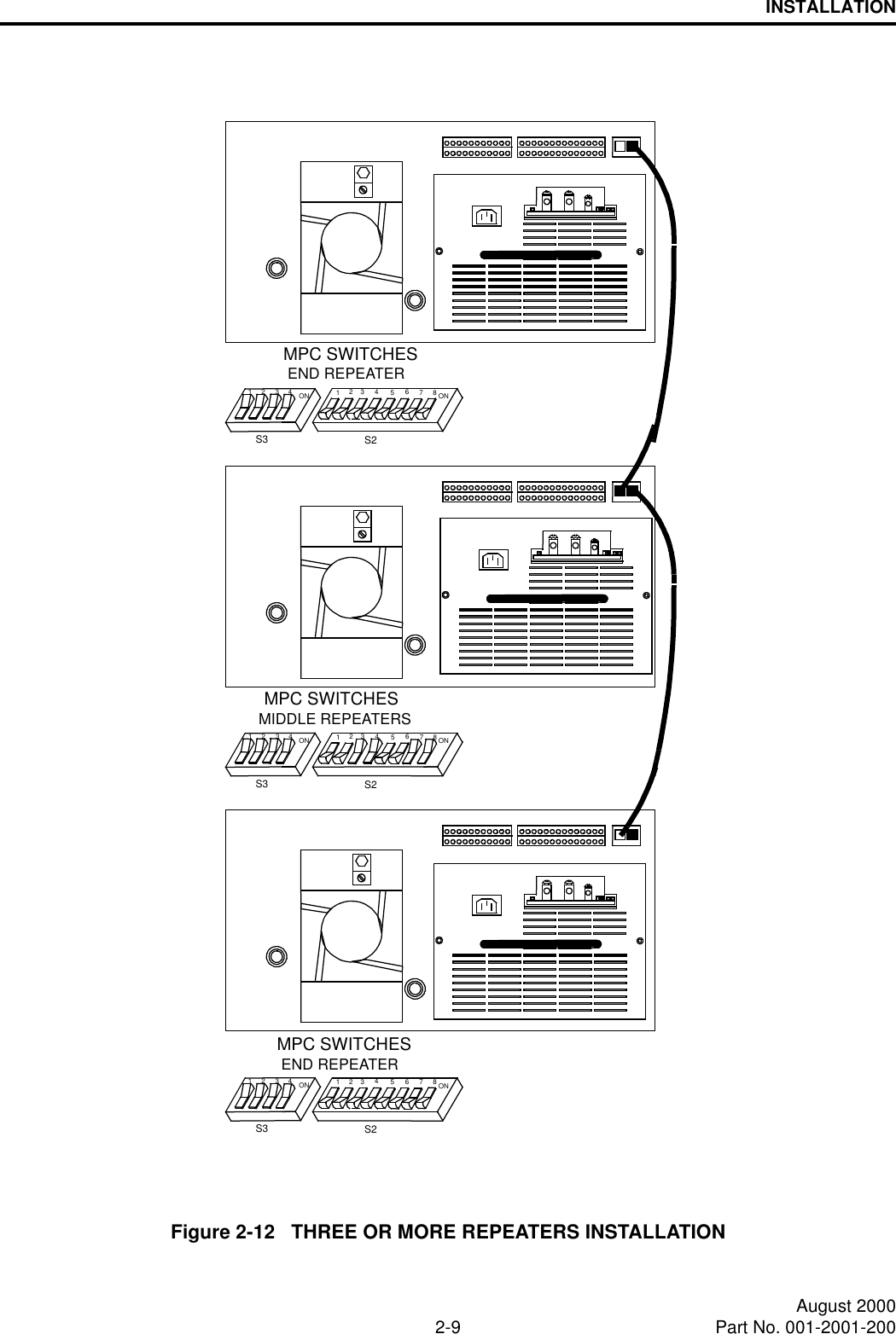
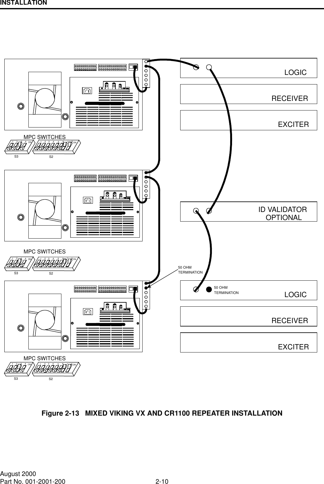
E F Johnson 2422001-1 Repeater User Manual

E. F. Johnson Company Repeater

manual

1-1 October 1995Part No. 001-2008-202VIKING® VXVHF LTR25W-110W RepeaterPart No. 242-20X1-213 First PrintingAugust 2000PRELIMINARY
1-3 October 1995Part No. 001-2008-202VIKING® VXVHF LTR REPEATERPART NO. 242-20X1-213Copyright 2000 by the E.F. Johnson CompanyThe E.F. Johnson Company designs and manufactures two-way radio equipment to serve a wide variety of communications needs. Johnson produces equipment for the mobile telephone and land mobile radio services which include business, indus-trial, government, public safety, and personal users. LAND MOBILE PRODUCT WARRANTYThe manufacturer’s warranty statement for this product is available from your product supplier or from the E.F. Johnson Com-pany, 299 Johnson Avenue, Box 1249, Waseca, MN 56093-0514. Phone (507) 835-6222.WARNINGThis device complies with Part 15 of the FCC rules.  Operation is subject to the condition that this device does not cause harm-ful interference.  In addition, changes or modification to this equipment not expressly approved by E. F. Johnson could void the user’s authority to operate this equipment (FCC rules, 47CFR Part 15.19).DO NOT allow the antenna to touch or come in very close proximity with the eyes, face, or any exposed body parts while the radio is transmitting.To comply with FCC RF exposure limits, DO NOT operate the transmitter of a stationary radio (base station or marine radio) when a person is within four (4) meters of the antenna.DO NOT operate the radio in explosive or flammable atmospheres. The transmitted radio energy could trigger blasting caps or cause an explosion.DO NOT operate the radio without the proper antenna installed.DO NOT allow children to operate transmitter equipped radio equipment.NOTE: The above warning list is not intended to include all hazards that may be encountered when using this radio.SAFETY INFORMATIONThe FCC has adopted a safety standard for human exposure to RF energy. Proper operation of this radio under normal conditions results in user exposure to RF energy below the Occupational Safety and Health Act and Federal Communication Commission limits.The information in this document is subject to change without notice.  E.F. Johnson Company will not be liable for any misunderstanding due to misinformation or errors found in this document.LTR, LTR-Net, Multi-Net, Viking Head/EFJohnson Logo, Call Guard and  SUMMIT are registered trademarks of E.F. Johnson Company  All other company and/or product names used in this manual are trademarks and/or registered trademarks of their respective manufacturer.
1-4October 1995Part No. 001-2008-202FCC EXPOSURE LIMITSThis fixed station radio transceiver was tested by the manufacturer with an appropriate antenna in order to verify compliance with Maximum Permissible Exposure (MPE) limits set under Section 2.1091 of the FCC Rules and Regulations. The guide-lines used in the evaluation are derived from Table 1 (B) titled “Limits For General Population/Uncontrolled Exposure” which is from FCC report OET bulletin #65.Table 2 lists the antennas recommended for use in the VHF frequency range. Each model of this radio was tested with the appropriate antenna listed. The antenna shall be mounted to a tower and be a minimum of 10 meters above the ground at the lowest point on the antenna. The radio manufacturer has determined that the user and service personnel should remain four (4) meters in distance away from the antenna when transmitting. By maintaining this distance, these individuals are not exposed to radio frequency energy or magnetic fields in excess of the guidelines set forth in Table 1 (B).NOTE: Other antennas or installation configurations that have not been tested may not comply with FCC RF exposure limits and therefore are not recommended.Table 1   (B)FCC Limits for Maximum Permissible Exposure (MPE)(B) Limits For General Population/Uncontrolled ExposureFrequency Range (MHz) Electric Field Strength (E) (V/m) Magnetic Field Strength (H) (A/m) Power Density (S) (mW/cm2)0.3 - 1.34 614 1.63 (100)*1.34 - 30 824/f 2.19/f (180/f2)*30 - 300 27.5 0.073 0.2300 - 1500 -- -- f/15001500 - 100,000 -- -- 1.0f = Frequency in MHz          *Plane-wave equivalent power density.Table 2   Recommended Antennas(Antenna Manufacturer - Decibel Products)Frequency Antenna Model No.132-144 MHz DB205E144-178 MHz DB205F
TABLE OF CONTENTS11 INTRODUCTION AND OPERATION1.1 SCOPE OF MANUAL. . . . . . . . . . . . . . . . . . . . . . . . . . . . . . . . . . . . . . . . . . . . . . . . . . . . . . . . . . . . . . . . . . . . . . . . .1-11.2 REPEATER DESCRIPTION . . . . . . . . . . . . . . . . . . . . . . . . . . . . . . . . . . . . . . . . . . . . . . . . . . . . . . . . . . . . . . . . . . .1-11.3 REPEATER IDENTIFICATION . . . . . . . . . . . . . . . . . . . . . . . . . . . . . . . . . . . . . . . . . . . . . . . . . . . . . . . . . . . . . . . . .1-11.4 MODEL NUMBER BREAKDOWN. . . . . . . . . . . . . . . . . . . . . . . . . . . . . . . . . . . . . . . . . . . . . . . . . . . . . . . . . . . . . .1-11.5 ACCESSORIES. . . . . . . . . . . . . . . . . . . . . . . . . . . . . . . . . . . . . . . . . . . . . . . . . . . . . . . . . . . . . . . . . . . . . . . . . . . . . .1-11.6 PRODUCT WARRANTY . . . . . . . . . . . . . . . . . . . . . . . . . . . . . . . . . . . . . . . . . . . . . . . . . . . . . . . . . . . . . . . . . . . . . .1-21.7 FACTORY CUSTOMER SERVICE  . . . . . . . . . . . . . . . . . . . . . . . . . . . . . . . . . . . . . . . . . . . . . . . . . . . . . . . . . . . . .1-21.8 FACTORY RETURNS  . . . . . . . . . . . . . . . . . . . . . . . . . . . . . . . . . . . . . . . . . . . . . . . . . . . . . . . . . . . . . . . . . . . . . . . .1-21.9 REPLACEMENT PARTS . . . . . . . . . . . . . . . . . . . . . . . . . . . . . . . . . . . . . . . . . . . . . . . . . . . . . . . . . . . . . . . . . . . . . .1-31.10 SOFTWARE UPDATES/REVISIONS  . . . . . . . . . . . . . . . . . . . . . . . . . . . . . . . . . . . . . . . . . . . . . . . . . . . . . . . . . . .1-31.11 REPEATER OPERATION . . . . . . . . . . . . . . . . . . . . . . . . . . . . . . . . . . . . . . . . . . . . . . . . . . . . . . . . . . . . . . . . . . . . .1-3MAIN PROCESSOR CARD (MPC) . . . . . . . . . . . . . . . . . . . . . . . . . . . . . . . . . . . . . . . . . . . . . . . . . . . . . . . . . . . . . .  1-3MAIN AUDIO CARD (MAC). . . . . . . . . . . . . . . . . . . . . . . . . . . . . . . . . . . . . . . . . . . . . . . . . . . . . . . . . . . . . . . . . . .  1-6INTERFACE ALARM CARD (IAC) . . . . . . . . . . . . . . . . . . . . . . . . . . . . . . . . . . . . . . . . . . . . . . . . . . . . . . . . . . . . .  1-6POWER SUPPLY  . . . . . . . . . . . . . . . . . . . . . . . . . . . . . . . . . . . . . . . . . . . . . . . . . . . . . . . . . . . . . . . . . . . . . . . . . . . .  1-71.12 REPEATER INFORMATION. . . . . . . . . . . . . . . . . . . . . . . . . . . . . . . . . . . . . . . . . . . . . . . . . . . . . . . . . . . . . . . . . . .1-7INTRODUCTION . . . . . . . . . . . . . . . . . . . . . . . . . . . . . . . . . . . . . . . . . . . . . . . . . . . . . . . . . . . . . . . . . . . . . . . . . . . .  1-7HOME REPEATERS. . . . . . . . . . . . . . . . . . . . . . . . . . . . . . . . . . . . . . . . . . . . . . . . . . . . . . . . . . . . . . . . . . . . . . . . . .  1-7INTER-REPEATER DATA COMMUNICATION. . . . . . . . . . . . . . . . . . . . . . . . . . . . . . . . . . . . . . . . . . . . . . . . . . .  1-7MOBILE TRANSCEIVERS . . . . . . . . . . . . . . . . . . . . . . . . . . . . . . . . . . . . . . . . . . . . . . . . . . . . . . . . . . . . . . . . . . . .  1-71.13 REPEATER DATA BUS SIGNALING . . . . . . . . . . . . . . . . . . . . . . . . . . . . . . . . . . . . . . . . . . . . . . . . . . . . . . . . . . .1-7GENERAL . . . . . . . . . . . . . . . . . . . . . . . . . . . . . . . . . . . . . . . . . . . . . . . . . . . . . . . . . . . . . . . . . . . . . . . . . . . . . . . . . .  1-7MOBILE DATA MESSAGE ORDER  . . . . . . . . . . . . . . . . . . . . . . . . . . . . . . . . . . . . . . . . . . . . . . . . . . . . . . . . . . . .  1-8ID VALIDATOR OPERATION . . . . . . . . . . . . . . . . . . . . . . . . . . . . . . . . . . . . . . . . . . . . . . . . . . . . . . . . . . . . . . . . .  1-82 INSTALLATION2.1 INTRODUCTION . . . . . . . . . . . . . . . . . . . . . . . . . . . . . . . . . . . . . . . . . . . . . . . . . . . . . . . . . . . . . . . . . . . . . . . . . . . . .2-1SITE PREPARATION AND ANTENNA INSTALLATION. . . . . . . . . . . . . . . . . . . . . . . . . . . . . . . . . . . . . . . . . . .  2-12.2 ENVIRONMENT. . . . . . . . . . . . . . . . . . . . . . . . . . . . . . . . . . . . . . . . . . . . . . . . . . . . . . . . . . . . . . . . . . . . . . . . . . . . . .2-12.3 VENTILATION . . . . . . . . . . . . . . . . . . . . . . . . . . . . . . . . . . . . . . . . . . . . . . . . . . . . . . . . . . . . . . . . . . . . . . . . . . . . . . .2-12.4 AC POWER  . . . . . . . . . . . . . . . . . . . . . . . . . . . . . . . . . . . . . . . . . . . . . . . . . . . . . . . . . . . . . . . . . . . . . . . . . . . . . . . . .2-22.5 BATTERY BACKUP. . . . . . . . . . . . . . . . . . . . . . . . . . . . . . . . . . . . . . . . . . . . . . . . . . . . . . . . . . . . . . . . . . . . . . . . . .2-22.6 800W POWER SUPPLY  . . . . . . . . . . . . . . . . . . . . . . . . . . . . . . . . . . . . . . . . . . . . . . . . . . . . . . . . . . . . . . . . . . . . . .2-2AC INPUT REQUIREMENTS . . . . . . . . . . . . . . . . . . . . . . . . . . . . . . . . . . . . . . . . . . . . . . . . . . . . . . . . . . . . . . . . . .  2-32.7 GROUNDING . . . . . . . . . . . . . . . . . . . . . . . . . . . . . . . . . . . . . . . . . . . . . . . . . . . . . . . . . . . . . . . . . . . . . . . . . . . . . . . .2-4PROTECTION GUIDELINES  . . . . . . . . . . . . . . . . . . . . . . . . . . . . . . . . . . . . . . . . . . . . . . . . . . . . . . . . . . . . . . . . . .  2-52.8 UNPACKING AND INSPECTION. . . . . . . . . . . . . . . . . . . . . . . . . . . . . . . . . . . . . . . . . . . . . . . . . . . . . . . . . . . . . . .2-52.9 REPEATER DATA BUS INSTALLATION  . . . . . . . . . . . . . . . . . . . . . . . . . . . . . . . . . . . . . . . . . . . . . . . . . . . . . . .2-6MPC DATA BUS SWITCH SETTINGS. . . . . . . . . . . . . . . . . . . . . . . . . . . . . . . . . . . . . . . . . . . . . . . . . . . . . . . . . . .  2-6MPC DATA BUS JUMPER SETTINGS. . . . . . . . . . . . . . . . . . . . . . . . . . . . . . . . . . . . . . . . . . . . . . . . . . . . . . . . . . .  2-62.10 CONNECTING RECEIVE AND TRANSMIT ANTENNAS . . . . . . . . . . . . . . . . . . . . . . . . . . . . . . . . . . . . . . . . . .2-73 SOFTWARE3.1 INTRODUCTION . . . . . . . . . . . . . . . . . . . . . . . . . . . . . . . . . . . . . . . . . . . . . . . . . . . . . . . . . . . . . . . . . . . . . . . . . . . . .3-1HOW TO USE THIS MANUAL . . . . . . . . . . . . . . . . . . . . . . . . . . . . . . . . . . . . . . . . . . . . . . . . . . . . . . . . . . . . . . . . .  3-1GETTING STARTED . . . . . . . . . . . . . . . . . . . . . . . . . . . . . . . . . . . . . . . . . . . . . . . . . . . . . . . . . . . . . . . . . . . . . . . . .  3-1COMPUTER DESCRIPTION . . . . . . . . . . . . . . . . . . . . . . . . . . . . . . . . . . . . . . . . . . . . . . . . . . . . . . . . . . . . . . . . . . .  3-1EEPROM DATA STORAGE  . . . . . . . . . . . . . . . . . . . . . . . . . . . . . . . . . . . . . . . . . . . . . . . . . . . . . . . . . . . . . . . . . . .  3-1COMMAND LINE OPTIONS. . . . . . . . . . . . . . . . . . . . . . . . . . . . . . . . . . . . . . . . . . . . . . . . . . . . . . . . . . . . . . . . . . .  3-2COLOR OR MONOCHROME OPERATION . . . . . . . . . . . . . . . . . . . . . . . . . . . . . . . . . . . . . . . . . . . . . . . . . . . . . .  3-2
TABLE OF CONTENTS (CONT.)23.2 REPEATER PROGRAM SOFTWARE. . . . . . . . . . . . . . . . . . . . . . . . . . . . . . . . . . . . . . . . . . . . . . . . . . . . . . . . . .  3-2INSTALLING THE SOFTWARE . . . . . . . . . . . . . . . . . . . . . . . . . . . . . . . . . . . . . . . . . . . . . . . . . . . . . . . . . . . . . . . .  3-2MINIMUM FREE MEMORY REQUIRED  . . . . . . . . . . . . . . . . . . . . . . . . . . . . . . . . . . . . . . . . . . . . . . . . . . . . . . . .  3-33.3 REPEATER PROGRAMMER . . . . . . . . . . . . . . . . . . . . . . . . . . . . . . . . . . . . . . . . . . . . . . . . . . . . . . . . . . . . . . . . .  3-3PROGRAM FILES . . . . . . . . . . . . . . . . . . . . . . . . . . . . . . . . . . . . . . . . . . . . . . . . . . . . . . . . . . . . . . . . . . . . . . . . . . . .  3-33.4 ALIGNMENT SOFTWARE. . . . . . . . . . . . . . . . . . . . . . . . . . . . . . . . . . . . . . . . . . . . . . . . . . . . . . . . . . . . . . . . . . . .  3-33.5 HELP  F1. . . . . . . . . . . . . . . . . . . . . . . . . . . . . . . . . . . . . . . . . . . . . . . . . . . . . . . . . . . . . . . . . . . . . . . . . . . . . . . . . . .  3-44 PULL DOWN MENUS4.1 MENU DISPLAYS . . . . . . . . . . . . . . . . . . . . . . . . . . . . . . . . . . . . . . . . . . . . . . . . . . . . . . . . . . . . . . . . . . . . . . . . . . .  4-14.2 FILE MENU. . . . . . . . . . . . . . . . . . . . . . . . . . . . . . . . . . . . . . . . . . . . . . . . . . . . . . . . . . . . . . . . . . . . . . . . . . . . . . . . .  4-1LOAD . . . . . . . . . . . . . . . . . . . . . . . . . . . . . . . . . . . . . . . . . . . . . . . . . . . . . . . . . . . . . . . . . . . . . . . . . . . . . . . . . . . . . .  4-1SAVE  . . . . . . . . . . . . . . . . . . . . . . . . . . . . . . . . . . . . . . . . . . . . . . . . . . . . . . . . . . . . . . . . . . . . . . . . . . . . . . . . . . . . . .  4-1SAVE AS . . . . . . . . . . . . . . . . . . . . . . . . . . . . . . . . . . . . . . . . . . . . . . . . . . . . . . . . . . . . . . . . . . . . . . . . . . . . . . . . . . .  4-1NEW . . . . . . . . . . . . . . . . . . . . . . . . . . . . . . . . . . . . . . . . . . . . . . . . . . . . . . . . . . . . . . . . . . . . . . . . . . . . . . . . . . . . . . .  4-2PRINT REPEATER CONFIGURATION . . . . . . . . . . . . . . . . . . . . . . . . . . . . . . . . . . . . . . . . . . . . . . . . . . . . . . . . . .  4-2DOS SHELL . . . . . . . . . . . . . . . . . . . . . . . . . . . . . . . . . . . . . . . . . . . . . . . . . . . . . . . . . . . . . . . . . . . . . . . . . . . . . . . . .  4-2QUIT (ALT X) . . . . . . . . . . . . . . . . . . . . . . . . . . . . . . . . . . . . . . . . . . . . . . . . . . . . . . . . . . . . . . . . . . . . . . . . . . . . . . .  4-24.3 EDIT . . . . . . . . . . . . . . . . . . . . . . . . . . . . . . . . . . . . . . . . . . . . . . . . . . . . . . . . . . . . . . . . . . . . . . . . . . . . . . . . . . . . . . .  4-3SETUP PARAMETERS. . . . . . . . . . . . . . . . . . . . . . . . . . . . . . . . . . . . . . . . . . . . . . . . . . . . . . . . . . . . . . . . . . . . . . . .  4-3SELECT REPEATER. . . . . . . . . . . . . . . . . . . . . . . . . . . . . . . . . . . . . . . . . . . . . . . . . . . . . . . . . . . . . . . . . . . . . . . . . .  4-4ALARM CONFIGURATION  . . . . . . . . . . . . . . . . . . . . . . . . . . . . . . . . . . . . . . . . . . . . . . . . . . . . . . . . . . . . . . . . . . .  4-4REPEATER TYPE . . . . . . . . . . . . . . . . . . . . . . . . . . . . . . . . . . . . . . . . . . . . . . . . . . . . . . . . . . . . . . . . . . . . . . . . . . . .  4-5DELETE REPEATER  . . . . . . . . . . . . . . . . . . . . . . . . . . . . . . . . . . . . . . . . . . . . . . . . . . . . . . . . . . . . . . . . . . . . . . . . .  4-5TELEPHONE PARAMETERS . . . . . . . . . . . . . . . . . . . . . . . . . . . . . . . . . . . . . . . . . . . . . . . . . . . . . . . . . . . . . . . . . .  4-64.4 TRANSFER. . . . . . . . . . . . . . . . . . . . . . . . . . . . . . . . . . . . . . . . . . . . . . . . . . . . . . . . . . . . . . . . . . . . . . . . . . . . . . . . .  4-6WRITE SETUP PARAMETERS . . . . . . . . . . . . . . . . . . . . . . . . . . . . . . . . . . . . . . . . . . . . . . . . . . . . . . . . . . . . . . . . .  4-6READ SETUP PARAMETERS. . . . . . . . . . . . . . . . . . . . . . . . . . . . . . . . . . . . . . . . . . . . . . . . . . . . . . . . . . . . . . . . . .  4-64.5 HARDWARE. . . . . . . . . . . . . . . . . . . . . . . . . . . . . . . . . . . . . . . . . . . . . . . . . . . . . . . . . . . . . . . . . . . . . . . . . . . . . . . .  4-7HSDB MONITOR  . . . . . . . . . . . . . . . . . . . . . . . . . . . . . . . . . . . . . . . . . . . . . . . . . . . . . . . . . . . . . . . . . . . . . . . . . . . .  4-7RECEIVE/TRANSMIT DATA . . . . . . . . . . . . . . . . . . . . . . . . . . . . . . . . . . . . . . . . . . . . . . . . . . . . . . . . . . . . . . . . . .  4-7RF DATA . . . . . . . . . . . . . . . . . . . . . . . . . . . . . . . . . . . . . . . . . . . . . . . . . . . . . . . . . . . . . . . . . . . . . . . . . . . . . . . . . . .  4-7REVISION/VERSION . . . . . . . . . . . . . . . . . . . . . . . . . . . . . . . . . . . . . . . . . . . . . . . . . . . . . . . . . . . . . . . . . . . . . . . . .  4-8MODE SELECT. . . . . . . . . . . . . . . . . . . . . . . . . . . . . . . . . . . . . . . . . . . . . . . . . . . . . . . . . . . . . . . . . . . . . . . . . . . . . .  4-84.6 TEST  . . . . . . . . . . . . . . . . . . . . . . . . . . . . . . . . . . . . . . . . . . . . . . . . . . . . . . . . . . . . . . . . . . . . . . . . . . . . . . . . . . . . . .  4-9POWER AMPLIFIER  . . . . . . . . . . . . . . . . . . . . . . . . . . . . . . . . . . . . . . . . . . . . . . . . . . . . . . . . . . . . . . . . . . . . . . . . .  4-9RECEIVER. . . . . . . . . . . . . . . . . . . . . . . . . . . . . . . . . . . . . . . . . . . . . . . . . . . . . . . . . . . . . . . . . . . . . . . . . . . . . . . . . .  4-9EXCITER . . . . . . . . . . . . . . . . . . . . . . . . . . . . . . . . . . . . . . . . . . . . . . . . . . . . . . . . . . . . . . . . . . . . . . . . . . . . . . . . . . .  4-9FULL REPEATER . . . . . . . . . . . . . . . . . . . . . . . . . . . . . . . . . . . . . . . . . . . . . . . . . . . . . . . . . . . . . . . . . . . . . . . . . . .  4-104.7 UTILITIES . . . . . . . . . . . . . . . . . . . . . . . . . . . . . . . . . . . . . . . . . . . . . . . . . . . . . . . . . . . . . . . . . . . . . . . . . . . . . . . . .  4-10COM PORT  . . . . . . . . . . . . . . . . . . . . . . . . . . . . . . . . . . . . . . . . . . . . . . . . . . . . . . . . . . . . . . . . . . . . . . . . . . . . . . . .  4-10DISPLAY MODE. . . . . . . . . . . . . . . . . . . . . . . . . . . . . . . . . . . . . . . . . . . . . . . . . . . . . . . . . . . . . . . . . . . . . . . . . . . .  4-10USER LEVEL. . . . . . . . . . . . . . . . . . . . . . . . . . . . . . . . . . . . . . . . . . . . . . . . . . . . . . . . . . . . . . . . . . . . . . . . . . . . . . .  4-105 REPEATER PROGRAMMING5.1 CREATING A NEW FILE . . . . . . . . . . . . . . . . . . . . . . . . . . . . . . . . . . . . . . . . . . . . . . . . . . . . . . . . . . . . . . . . . . . . .  5-1SELECT REPEATER TO EDIT  . . . . . . . . . . . . . . . . . . . . . . . . . . . . . . . . . . . . . . . . . . . . . . . . . . . . . . . . . . . . . . . . .  5-15.2 ADDING A REPEATER TO A FILE . . . . . . . . . . . . . . . . . . . . . . . . . . . . . . . . . . . . . . . . . . . . . . . . . . . . . . . . . . . .  5-1
TABLE OF CONTENTS (CONT.)36 CIRCUIT DESCRIPTION6.1 RECEIVER . . . . . . . . . . . . . . . . . . . . . . . . . . . . . . . . . . . . . . . . . . . . . . . . . . . . . . . . . . . . . . . . . . . . . . . . . . . . . . . . . .6-1INTRODUCTION . . . . . . . . . . . . . . . . . . . . . . . . . . . . . . . . . . . . . . . . . . . . . . . . . . . . . . . . . . . . . . . . . . . . . . . . . . . .  6-1REGULATED VOLTAGE SUPPLIES . . . . . . . . . . . . . . . . . . . . . . . . . . . . . . . . . . . . . . . . . . . . . . . . . . . . . . . . . . . .  6-1HELICAL FILTERS, RF AMPLIFIER . . . . . . . . . . . . . . . . . . . . . . . . . . . . . . . . . . . . . . . . . . . . . . . . . . . . . . . . . . . .  6-112.5 kHz IF. . . . . . . . . . . . . . . . . . . . . . . . . . . . . . . . . . . . . . . . . . . . . . . . . . . . . . . . . . . . . . . . . . . . . . . . . . . . . . . . . .  6-125 kHz IF . . . . . . . . . . . . . . . . . . . . . . . . . . . . . . . . . . . . . . . . . . . . . . . . . . . . . . . . . . . . . . . . . . . . . . . . . . . . . . . . . . .  6-3VCO . . . . . . . . . . . . . . . . . . . . . . . . . . . . . . . . . . . . . . . . . . . . . . . . . . . . . . . . . . . . . . . . . . . . . . . . . . . . . . . . . . . . . . .  6-4ACTIVE FILTER. . . . . . . . . . . . . . . . . . . . . . . . . . . . . . . . . . . . . . . . . . . . . . . . . . . . . . . . . . . . . . . . . . . . . . . . . . . . .  6-4BUFFER. . . . . . . . . . . . . . . . . . . . . . . . . . . . . . . . . . . . . . . . . . . . . . . . . . . . . . . . . . . . . . . . . . . . . . . . . . . . . . . . . . . .  6-5SYNTHESIZER . . . . . . . . . . . . . . . . . . . . . . . . . . . . . . . . . . . . . . . . . . . . . . . . . . . . . . . . . . . . . . . . . . . . . . . . . . . . . .  6-5BUFFER AMPLIFIER. . . . . . . . . . . . . . . . . . . . . . . . . . . . . . . . . . . . . . . . . . . . . . . . . . . . . . . . . . . . . . . . . . . . . . . . .  6-7LOCK DETECT. . . . . . . . . . . . . . . . . . . . . . . . . . . . . . . . . . . . . . . . . . . . . . . . . . . . . . . . . . . . . . . . . . . . . . . . . . . . . .  6-7CHARGE PUMP, LOOP FILTER. . . . . . . . . . . . . . . . . . . . . . . . . . . . . . . . . . . . . . . . . . . . . . . . . . . . . . . . . . . . . . . .  6-7VOLTAGE MULTIPLIER  . . . . . . . . . . . . . . . . . . . . . . . . . . . . . . . . . . . . . . . . . . . . . . . . . . . . . . . . . . . . . . . . . . . . .  6-7BUFFER AMPLIFIER. . . . . . . . . . . . . . . . . . . . . . . . . . . . . . . . . . . . . . . . . . . . . . . . . . . . . . . . . . . . . . . . . . . . . . . . .  6-7FIRST AND SECOND INJECTION AMPLIFIERS. . . . . . . . . . . . . . . . . . . . . . . . . . . . . . . . . . . . . . . . . . . . . . . . . .  6-86.2 EXCITER. . . . . . . . . . . . . . . . . . . . . . . . . . . . . . . . . . . . . . . . . . . . . . . . . . . . . . . . . . . . . . . . . . . . . . . . . . . . . . . . . . . .6-8VCO (A007) . . . . . . . . . . . . . . . . . . . . . . . . . . . . . . . . . . . . . . . . . . . . . . . . . . . . . . . . . . . . . . . . . . . . . . . . . . . . . . . . .  6-8VCO BUFFER . . . . . . . . . . . . . . . . . . . . . . . . . . . . . . . . . . . . . . . . . . . . . . . . . . . . . . . . . . . . . . . . . . . . . . . . . . . . . . .  6-8VCO/TCXO FREQUENCY MODULATION. . . . . . . . . . . . . . . . . . . . . . . . . . . . . . . . . . . . . . . . . . . . . . . . . . . . . . .  6-8SYNTHESIZER . . . . . . . . . . . . . . . . . . . . . . . . . . . . . . . . . . . . . . . . . . . . . . . . . . . . . . . . . . . . . . . . . . . . . . . . . . . . . .  6-9BUFFER AMPLIFIER. . . . . . . . . . . . . . . . . . . . . . . . . . . . . . . . . . . . . . . . . . . . . . . . . . . . . . . . . . . . . . . . . . . . . . . .  6-10BUFFER AMPLIFIER. . . . . . . . . . . . . . . . . . . . . . . . . . . . . . . . . . . . . . . . . . . . . . . . . . . . . . . . . . . . . . . . . . . . . . . .  6-10LOCK DETECT. . . . . . . . . . . . . . . . . . . . . . . . . . . . . . . . . . . . . . . . . . . . . . . . . . . . . . . . . . . . . . . . . . . . . . . . . . . . .  6-10CHARGE PUMP, LOOP FILTER. . . . . . . . . . . . . . . . . . . . . . . . . . . . . . . . . . . . . . . . . . . . . . . . . . . . . . . . . . . . . . .  6-11BUFFER AMPLIFIER. . . . . . . . . . . . . . . . . . . . . . . . . . . . . . . . . . . . . . . . . . . . . . . . . . . . . . . . . . . . . . . . . . . . . . . .  6-11RF AMPLIFIERS. . . . . . . . . . . . . . . . . . . . . . . . . . . . . . . . . . . . . . . . . . . . . . . . . . . . . . . . . . . . . . . . . . . . . . . . . . . .  6-116.3 110W POWER AMPLIFIER. . . . . . . . . . . . . . . . . . . . . . . . . . . . . . . . . . . . . . . . . . . . . . . . . . . . . . . . . . . . . . . . . . .6-11AMPLIFIER/PREDRIVER . . . . . . . . . . . . . . . . . . . . . . . . . . . . . . . . . . . . . . . . . . . . . . . . . . . . . . . . . . . . . . . . . . . .  6-11DRIVER . . . . . . . . . . . . . . . . . . . . . . . . . . . . . . . . . . . . . . . . . . . . . . . . . . . . . . . . . . . . . . . . . . . . . . . . . . . . . . . . . . .  6-11FINAL AMPLIFIERS . . . . . . . . . . . . . . . . . . . . . . . . . . . . . . . . . . . . . . . . . . . . . . . . . . . . . . . . . . . . . . . . . . . . . . . .  6-12POWER DETECTORS . . . . . . . . . . . . . . . . . . . . . . . . . . . . . . . . . . . . . . . . . . . . . . . . . . . . . . . . . . . . . . . . . . . . . . .  6-12THERMAL SENSOR  . . . . . . . . . . . . . . . . . . . . . . . . . . . . . . . . . . . . . . . . . . . . . . . . . . . . . . . . . . . . . . . . . . . . . . . .  6-12FORWARD/REVERSE POWER DETECT, CIRCULATOR, LOW-PASS FILTER . . . . . . . . . . . . . . . . . . . . . . .  6-126.4 RF INTERFACE BOARD. . . . . . . . . . . . . . . . . . . . . . . . . . . . . . . . . . . . . . . . . . . . . . . . . . . . . . . . . . . . . . . . . . . . .6-13POWER CONNECTOR. . . . . . . . . . . . . . . . . . . . . . . . . . . . . . . . . . . . . . . . . . . . . . . . . . . . . . . . . . . . . . . . . . . . . . .  6-13SIGNAL CONNECTOR (J101). . . . . . . . . . . . . . . . . . . . . . . . . . . . . . . . . . . . . . . . . . . . . . . . . . . . . . . . . . . . . . . . .  6-13FAN CONNECTOR (J104) . . . . . . . . . . . . . . . . . . . . . . . . . . . . . . . . . . . . . . . . . . . . . . . . . . . . . . . . . . . . . . . . . . . .  6-15POWER AMPLIFIER CONNECTIONS. . . . . . . . . . . . . . . . . . . . . . . . . . . . . . . . . . . . . . . . . . . . . . . . . . . . . . . . . .  6-15EXCITER CONNECTOR (J102). . . . . . . . . . . . . . . . . . . . . . . . . . . . . . . . . . . . . . . . . . . . . . . . . . . . . . . . . . . . . . . .  6-16RECEIVER CONNECTOR (J103) . . . . . . . . . . . . . . . . . . . . . . . . . . . . . . . . . . . . . . . . . . . . . . . . . . . . . . . . . . . . . .  6-176.5 800W POWER SUPPLY  . . . . . . . . . . . . . . . . . . . . . . . . . . . . . . . . . . . . . . . . . . . . . . . . . . . . . . . . . . . . . . . . . . . . .6-20FILTER BOARD . . . . . . . . . . . . . . . . . . . . . . . . . . . . . . . . . . . . . . . . . . . . . . . . . . . . . . . . . . . . . . . . . . . . . . . . . . . .  6-20POWER FACTOR CORRECTION. . . . . . . . . . . . . . . . . . . . . . . . . . . . . . . . . . . . . . . . . . . . . . . . . . . . . . . . . . . . . .  6-20MAIN PULSE WIDTH MODULATOR . . . . . . . . . . . . . . . . . . . . . . . . . . . . . . . . . . . . . . . . . . . . . . . . . . . . . . . . . .  6-20SYNCHRONIZING CIRCUITS . . . . . . . . . . . . . . . . . . . . . . . . . . . . . . . . . . . . . . . . . . . . . . . . . . . . . . . . . . . . . . . .  6-22FAN AND THERMAL SHUTDOWN  . . . . . . . . . . . . . . . . . . . . . . . . . . . . . . . . . . . . . . . . . . . . . . . . . . . . . . . . . . .  6-22+15V CONVERTER . . . . . . . . . . . . . . . . . . . . . . . . . . . . . . . . . . . . . . . . . . . . . . . . . . . . . . . . . . . . . . . . . . . . . . . . .  6-23+5V CONVERTER . . . . . . . . . . . . . . . . . . . . . . . . . . . . . . . . . . . . . . . . . . . . . . . . . . . . . . . . . . . . . . . . . . . . . . . . . .  6-23-5V CONVERTER. . . . . . . . . . . . . . . . . . . . . . . . . . . . . . . . . . . . . . . . . . . . . . . . . . . . . . . . . . . . . . . . . . . . . . . . . . .  6-23POWER SUPPLY REPAIR AND ALIGNMENT. . . . . . . . . . . . . . . . . . . . . . . . . . . . . . . . . . . . . . . . . . . . . . . . . . .  6-23
TABLE OF CONTENTS (CONT.)46.6 BATTERY BACK-UP MODULE . . . . . . . . . . . . . . . . . . . . . . . . . . . . . . . . . . . . . . . . . . . . . . . . . . . . . . . . . . . . . .  6-24OPERATION . . . . . . . . . . . . . . . . . . . . . . . . . . . . . . . . . . . . . . . . . . . . . . . . . . . . . . . . . . . . . . . . . . . . . . . . . . . . . . .  6-24CHARGER . . . . . . . . . . . . . . . . . . . . . . . . . . . . . . . . . . . . . . . . . . . . . . . . . . . . . . . . . . . . . . . . . . . . . . . . . . . . . . . . .  6-24REVERSE BATTERY PROTECTION . . . . . . . . . . . . . . . . . . . . . . . . . . . . . . . . . . . . . . . . . . . . . . . . . . . . . . . . . . .  6-25ENGAGING THE RELAY  . . . . . . . . . . . . . . . . . . . . . . . . . . . . . . . . . . . . . . . . . . . . . . . . . . . . . . . . . . . . . . . . . . . .  6-25OVER/UNDERVOLTAGE SHUTDOWN . . . . . . . . . . . . . . . . . . . . . . . . . . . . . . . . . . . . . . . . . . . . . . . . . . . . . . . .  6-25BBM FAN CONTROL. . . . . . . . . . . . . . . . . . . . . . . . . . . . . . . . . . . . . . . . . . . . . . . . . . . . . . . . . . . . . . . . . . . . . . . .  6-266.7 CARD RACK  . . . . . . . . . . . . . . . . . . . . . . . . . . . . . . . . . . . . . . . . . . . . . . . . . . . . . . . . . . . . . . . . . . . . . . . . . . . . . .  6-266.9 EXTERNAL CONNECTOR BOARD  . . . . . . . . . . . . . . . . . . . . . . . . . . . . . . . . . . . . . . . . . . . . . . . . . . . . . . . . . .  6-276.10 MAIN PROCESSOR CARD. . . . . . . . . . . . . . . . . . . . . . . . . . . . . . . . . . . . . . . . . . . . . . . . . . . . . . . . . . . . . . . . . .  6-28INTRODUCTION  . . . . . . . . . . . . . . . . . . . . . . . . . . . . . . . . . . . . . . . . . . . . . . . . . . . . . . . . . . . . . . . . . . . . . . . . . . .  6-28MAIN CONTROLLER MICROPROCESSOR . . . . . . . . . . . . . . . . . . . . . . . . . . . . . . . . . . . . . . . . . . . . . . . . . . . . .  6-29HIGH SPEED DATA BUS MICROPROCESSOR (U13). . . . . . . . . . . . . . . . . . . . . . . . . . . . . . . . . . . . . . . . . . . . . 6-29CHIP SELECT DECODERS (U15/U4) . . . . . . . . . . . . . . . . . . . . . . . . . . . . . . . . . . . . . . . . . . . . . . . . . . . . . . . . . . .  6-30P1 SIGNAL CONNECTOR . . . . . . . . . . . . . . . . . . . . . . . . . . . . . . . . . . . . . . . . . . . . . . . . . . . . . . . . . . . . . . . . . . . .  6-30J1 COMPUTER CONNECTOR. . . . . . . . . . . . . . . . . . . . . . . . . . . . . . . . . . . . . . . . . . . . . . . . . . . . . . . . . . . . . . . . .  6-31J2 MEMORY SELECT  . . . . . . . . . . . . . . . . . . . . . . . . . . . . . . . . . . . . . . . . . . . . . . . . . . . . . . . . . . . . . . . . . . . . . . .  6-31J3 BAUD RATE . . . . . . . . . . . . . . . . . . . . . . . . . . . . . . . . . . . . . . . . . . . . . . . . . . . . . . . . . . . . . . . . . . . . . . . . . . . . .  6-31S2/S3 HSDB SETTINGS . . . . . . . . . . . . . . . . . . . . . . . . . . . . . . . . . . . . . . . . . . . . . . . . . . . . . . . . . . . . . . . . . . . . . .  6-31J4 EPROM MEMORY LOADING . . . . . . . . . . . . . . . . . . . . . . . . . . . . . . . . . . . . . . . . . . . . . . . . . . . . . . . . . . . . . .  6-31J5 HSDB SPEED  . . . . . . . . . . . . . . . . . . . . . . . . . . . . . . . . . . . . . . . . . . . . . . . . . . . . . . . . . . . . . . . . . . . . . . . . . . . .  6-31J6 WATCHDOG. . . . . . . . . . . . . . . . . . . . . . . . . . . . . . . . . . . . . . . . . . . . . . . . . . . . . . . . . . . . . . . . . . . . . . . . . . . . .  6-316.11 MAIN AUDIO CARD . . . . . . . . . . . . . . . . . . . . . . . . . . . . . . . . . . . . . . . . . . . . . . . . . . . . . . . . . . . . . . . . . . . . . . . .  6-32INTRODUCTION  . . . . . . . . . . . . . . . . . . . . . . . . . . . . . . . . . . . . . . . . . . . . . . . . . . . . . . . . . . . . . . . . . . . . . . . . . . .  6-32AUDIO/DATA MICROPROCESSOR  . . . . . . . . . . . . . . . . . . . . . . . . . . . . . . . . . . . . . . . . . . . . . . . . . . . . . . . . . . .  6-32RECEIVE AUDIO . . . . . . . . . . . . . . . . . . . . . . . . . . . . . . . . . . . . . . . . . . . . . . . . . . . . . . . . . . . . . . . . . . . . . . . . . . .  6-32RECEIVE SQUELCH CIRCUITRY . . . . . . . . . . . . . . . . . . . . . . . . . . . . . . . . . . . . . . . . . . . . . . . . . . . . . . . . . . . . .  6-33RECEIVE DATA CIRCUITRY. . . . . . . . . . . . . . . . . . . . . . . . . . . . . . . . . . . . . . . . . . . . . . . . . . . . . . . . . . . . . . . . .  6-33RECEIVE AUDIO PROCESSING  . . . . . . . . . . . . . . . . . . . . . . . . . . . . . . . . . . . . . . . . . . . . . . . . . . . . . . . . . . . . . .  6-33VOTER AUDIO . . . . . . . . . . . . . . . . . . . . . . . . . . . . . . . . . . . . . . . . . . . . . . . . . . . . . . . . . . . . . . . . . . . . . . . . . . . . .  6-34COMPANDOR OPTION . . . . . . . . . . . . . . . . . . . . . . . . . . . . . . . . . . . . . . . . . . . . . . . . . . . . . . . . . . . . . . . . . . . . . .  6-34TRANSMIT AUDIO  . . . . . . . . . . . . . . . . . . . . . . . . . . . . . . . . . . . . . . . . . . . . . . . . . . . . . . . . . . . . . . . . . . . . . . . . .  6-34TRANSMIT AUDIO PROCESSING. . . . . . . . . . . . . . . . . . . . . . . . . . . . . . . . . . . . . . . . . . . . . . . . . . . . . . . . . . . . .  6-34TRANSMIT DATA AND CWID PROCESSING . . . . . . . . . . . . . . . . . . . . . . . . . . . . . . . . . . . . . . . . . . . . . . . . . . .  6-35P101 SIGNALING CONNECTOR  . . . . . . . . . . . . . . . . . . . . . . . . . . . . . . . . . . . . . . . . . . . . . . . . . . . . . . . . . . . . . .  6-35P100 EXTERNAL OUTPUTS . . . . . . . . . . . . . . . . . . . . . . . . . . . . . . . . . . . . . . . . . . . . . . . . . . . . . . . . . . . . . . . . . .  6-36J100 A D LEVEL TEST POINT  . . . . . . . . . . . . . . . . . . . . . . . . . . . . . . . . . . . . . . . . . . . . . . . . . . . . . . . . . . . . . . . .  6-37J101 SPEAKER/MICROPHONE. . . . . . . . . . . . . . . . . . . . . . . . . . . . . . . . . . . . . . . . . . . . . . . . . . . . . . . . . . . . . . . .  6-37J102 LOCAL MICROPHONE . . . . . . . . . . . . . . . . . . . . . . . . . . . . . . . . . . . . . . . . . . . . . . . . . . . . . . . . . . . . . . . . . .  6-37J103 GROUND. . . . . . . . . . . . . . . . . . . . . . . . . . . . . . . . . . . . . . . . . . . . . . . . . . . . . . . . . . . . . . . . . . . . . . . . . . . . . .  6-37J104 EXTERNAL SPEAKER . . . . . . . . . . . . . . . . . . . . . . . . . . . . . . . . . . . . . . . . . . . . . . . . . . . . . . . . . . . . . . . . . .  6-37J105 WATCH DOG . . . . . . . . . . . . . . . . . . . . . . . . . . . . . . . . . . . . . . . . . . . . . . . . . . . . . . . . . . . . . . . . . . . . . . . . . .  6-37J106 TX DATA PATH . . . . . . . . . . . . . . . . . . . . . . . . . . . . . . . . . . . . . . . . . . . . . . . . . . . . . . . . . . . . . . . . . . . . . . . .  6-37A301 COMPANDOR CONNECTIONS . . . . . . . . . . . . . . . . . . . . . . . . . . . . . . . . . . . . . . . . . . . . . . . . . . . . . . . . . .  6-376.12 INTERFACE ALARM CARD . . . . . . . . . . . . . . . . . . . . . . . . . . . . . . . . . . . . . . . . . . . . . . . . . . . . . . . . . . . . . . . . .  6-38RELAY OUTPUTS  . . . . . . . . . . . . . . . . . . . . . . . . . . . . . . . . . . . . . . . . . . . . . . . . . . . . . . . . . . . . . . . . . . . . . . . . . .  6-38ISOLATED INPUTS . . . . . . . . . . . . . . . . . . . . . . . . . . . . . . . . . . . . . . . . . . . . . . . . . . . . . . . . . . . . . . . . . . . . . . . . .  6-38ALARM INDICATORS. . . . . . . . . . . . . . . . . . . . . . . . . . . . . . . . . . . . . . . . . . . . . . . . . . . . . . . . . . . . . . . . . . . . . . .  6-39ALARM FUNCTIONS. . . . . . . . . . . . . . . . . . . . . . . . . . . . . . . . . . . . . . . . . . . . . . . . . . . . . . . . . . . . . . . . . . . . . . . .  6-39P500 SIGNALING CONNECTOR  . . . . . . . . . . . . . . . . . . . . . . . . . . . . . . . . . . . . . . . . . . . . . . . . . . . . . . . . . . . . . .  6-40P501 EXTERNAL OUTPUTS . . . . . . . . . . . . . . . . . . . . . . . . . . . . . . . . . . . . . . . . . . . . . . . . . . . . . . . . . . . . . . . . . .  6-41J500 A D LEVEL TEST POINT  . . . . . . . . . . . . . . . . . . . . . . . . . . . . . . . . . . . . . . . . . . . . . . . . . . . . . . . . . . . . . . . .  6-43J501 GROUND. . . . . . . . . . . . . . . . . . . . . . . . . . . . . . . . . . . . . . . . . . . . . . . . . . . . . . . . . . . . . . . . . . . . . . . . . . . . . .  6-43J502 +15V. . . . . . . . . . . . . . . . . . . . . . . . . . . . . . . . . . . . . . . . . . . . . . . . . . . . . . . . . . . . . . . . . . . . . . . . . . . . . . . . . .  6-43POWER SWITCH  . . . . . . . . . . . . . . . . . . . . . . . . . . . . . . . . . . . . . . . . . . . . . . . . . . . . . . . . . . . . . . . . . . . . . . . . . . .  6-43J505 SQUELCH ENABLE OUTPUT . . . . . . . . . . . . . . . . . . . . . . . . . . . . . . . . . . . . . . . . . . . . . . . . . . . . . . . . . . . .  6-43
TABLE OF CONTENTS (CONT.)57 ALIGNMENT AND TEST PROCEDURES7.1 RECEIVER ALIGNMENT. . . . . . . . . . . . . . . . . . . . . . . . . . . . . . . . . . . . . . . . . . . . . . . . . . . . . . . . . . . . . . . . . . . . . .7-1PRETEST . . . . . . . . . . . . . . . . . . . . . . . . . . . . . . . . . . . . . . . . . . . . . . . . . . . . . . . . . . . . . . . . . . . . . . . . . . . . . . . . . . .  7-1VOLTAGE MEASUREMENTS . . . . . . . . . . . . . . . . . . . . . . . . . . . . . . . . . . . . . . . . . . . . . . . . . . . . . . . . . . . . . . . . .  7-1PROGRAM TUNE-UP CHANNEL  . . . . . . . . . . . . . . . . . . . . . . . . . . . . . . . . . . . . . . . . . . . . . . . . . . . . . . . . . . . . . .  7-1RECEIVER FREQUENCY ADJUST . . . . . . . . . . . . . . . . . . . . . . . . . . . . . . . . . . . . . . . . . . . . . . . . . . . . . . . . . . . . .  7-2VCO TEST . . . . . . . . . . . . . . . . . . . . . . . . . . . . . . . . . . . . . . . . . . . . . . . . . . . . . . . . . . . . . . . . . . . . . . . . . . . . . . . . . .  7-2FRONT END ADJUSTMENTS  . . . . . . . . . . . . . . . . . . . . . . . . . . . . . . . . . . . . . . . . . . . . . . . . . . . . . . . . . . . . . . . . .  7-2AUDIO DISTORTION  . . . . . . . . . . . . . . . . . . . . . . . . . . . . . . . . . . . . . . . . . . . . . . . . . . . . . . . . . . . . . . . . . . . . . . . .  7-37.2 EXCITER ALIGNMENT . . . . . . . . . . . . . . . . . . . . . . . . . . . . . . . . . . . . . . . . . . . . . . . . . . . . . . . . . . . . . . . . . . . . . . .7-4PRETEST . . . . . . . . . . . . . . . . . . . . . . . . . . . . . . . . . . . . . . . . . . . . . . . . . . . . . . . . . . . . . . . . . . . . . . . . . . . . . . . . . . .  7-4VOLTAGE MEASUREMENTS . . . . . . . . . . . . . . . . . . . . . . . . . . . . . . . . . . . . . . . . . . . . . . . . . . . . . . . . . . . . . . . . .  7-4PROGRAM TUNE-UP CHANNEL  . . . . . . . . . . . . . . . . . . . . . . . . . . . . . . . . . . . . . . . . . . . . . . . . . . . . . . . . . . . . . .  7-4VCO TEST . . . . . . . . . . . . . . . . . . . . . . . . . . . . . . . . . . . . . . . . . . . . . . . . . . . . . . . . . . . . . . . . . . . . . . . . . . . . . . . . . .  7-5TCXO FREQUENCY ADJUST  . . . . . . . . . . . . . . . . . . . . . . . . . . . . . . . . . . . . . . . . . . . . . . . . . . . . . . . . . . . . . . . . .  7-5TRANSMIT MODULATION ADJUST . . . . . . . . . . . . . . . . . . . . . . . . . . . . . . . . . . . . . . . . . . . . . . . . . . . . . . . . . . .  7-57.3 110W POWER AMPLIFIER ALIGNMENT . . . . . . . . . . . . . . . . . . . . . . . . . . . . . . . . . . . . . . . . . . . . . . . . . . . . . . .7-6INTRODUCTION . . . . . . . . . . . . . . . . . . . . . . . . . . . . . . . . . . . . . . . . . . . . . . . . . . . . . . . . . . . . . . . . . . . . . . . . . . . .  7-6DRIVER TUNING AND LIMIT ADJUSTMENTS . . . . . . . . . . . . . . . . . . . . . . . . . . . . . . . . . . . . . . . . . . . . . . . . . .  7-6POWER AMPLIFIER TUNING . . . . . . . . . . . . . . . . . . . . . . . . . . . . . . . . . . . . . . . . . . . . . . . . . . . . . . . . . . . . . . . . .  7-67.4 FULL REPEATER ALIGNMENT  . . . . . . . . . . . . . . . . . . . . . . . . . . . . . . . . . . . . . . . . . . . . . . . . . . . . . . . . . . . . . .7-11PERFORMANCE TEST PROGRAM . . . . . . . . . . . . . . . . . . . . . . . . . . . . . . . . . . . . . . . . . . . . . . . . . . . . . . . . . . . .  7-11REPEATER SETUP. . . . . . . . . . . . . . . . . . . . . . . . . . . . . . . . . . . . . . . . . . . . . . . . . . . . . . . . . . . . . . . . . . . . . . . . . .  7-11TRANSMITTER TEST/ADJUSTMENTS . . . . . . . . . . . . . . . . . . . . . . . . . . . . . . . . . . . . . . . . . . . . . . . . . . . . . . . .  7-11RECEIVER TESTS/ADJUSTMENT  . . . . . . . . . . . . . . . . . . . . . . . . . . . . . . . . . . . . . . . . . . . . . . . . . . . . . . . . . . . .  7-11TRANSMIT AUDIO/DATA LEVEL ADJUSTMENTS. . . . . . . . . . . . . . . . . . . . . . . . . . . . . . . . . . . . . . . . . . . . . .  7-13VOTER AUDIO LEVEL ADJUSTMENT . . . . . . . . . . . . . . . . . . . . . . . . . . . . . . . . . . . . . . . . . . . . . . . . . . . . . . . .  7-15AUDIO/DATA LEVEL ADJUSTMENTS . . . . . . . . . . . . . . . . . . . . . . . . . . . . . . . . . . . . . . . . . . . . . . . . . . . . . . . .  7-15REPEATER OPERATION  . . . . . . . . . . . . . . . . . . . . . . . . . . . . . . . . . . . . . . . . . . . . . . . . . . . . . . . . . . . . . . . . . . . .  7-168 SERVICING8.1 INTRODUCTION . . . . . . . . . . . . . . . . . . . . . . . . . . . . . . . . . . . . . . . . . . . . . . . . . . . . . . . . . . . . . . . . . . . . . . . . . . . . .8-1PERIODIC CHECKS. . . . . . . . . . . . . . . . . . . . . . . . . . . . . . . . . . . . . . . . . . . . . . . . . . . . . . . . . . . . . . . . . . . . . . . . . .  8-1SURFACE-MOUNTED COMPONENTS. . . . . . . . . . . . . . . . . . . . . . . . . . . . . . . . . . . . . . . . . . . . . . . . . . . . . . . . . .  8-1SCHEMATIC DIAGRAMS AND COMPONENT LAYOUTS . . . . . . . . . . . . . . . . . . . . . . . . . . . . . . . . . . . . . . . . .  8-1REPLACEMENT PARTS LIST . . . . . . . . . . . . . . . . . . . . . . . . . . . . . . . . . . . . . . . . . . . . . . . . . . . . . . . . . . . . . . . . .  8-1TCXO MODULES NOT SERVICEABLE . . . . . . . . . . . . . . . . . . . . . . . . . . . . . . . . . . . . . . . . . . . . . . . . . . . . . . . . .  8-18.2 SYNTHESIZER SERVICING. . . . . . . . . . . . . . . . . . . . . . . . . . . . . . . . . . . . . . . . . . . . . . . . . . . . . . . . . . . . . . . . . . .8-1INTRODUCTION . . . . . . . . . . . . . . . . . . . . . . . . . . . . . . . . . . . . . . . . . . . . . . . . . . . . . . . . . . . . . . . . . . . . . . . . . . . .  8-1TCXO MODULE . . . . . . . . . . . . . . . . . . . . . . . . . . . . . . . . . . . . . . . . . . . . . . . . . . . . . . . . . . . . . . . . . . . . . . . . . . . . .  8-2VOLTAGE CONTROLLED OSCILLATOR (VCO) . . . . . . . . . . . . . . . . . . . . . . . . . . . . . . . . . . . . . . . . . . . . . . . . .  8-2INTERNAL PRESCALER  . . . . . . . . . . . . . . . . . . . . . . . . . . . . . . . . . . . . . . . . . . . . . . . . . . . . . . . . . . . . . . . . . . . . .  8-2CALCULATING  "N " AND  "A " COUNTER DIVIDE NUMBERS. . . . . . . . . . . . . . . . . . . . . . . . . . . . . . . . . . . .  8-38.3 RECEIVER SERVICING. . . . . . . . . . . . . . . . . . . . . . . . . . . . . . . . . . . . . . . . . . . . . . . . . . . . . . . . . . . . . . . . . . . . . . .8-38.4 TRANSMITTER SERVICING  . . . . . . . . . . . . . . . . . . . . . . . . . . . . . . . . . . . . . . . . . . . . . . . . . . . . . . . . . . . . . . . . . .8-38.5 POWER SUPPLY SERVICING. . . . . . . . . . . . . . . . . . . . . . . . . . . . . . . . . . . . . . . . . . . . . . . . . . . . . . . . . . . . . . . . .8-3VOLTAGE CHECKS  . . . . . . . . . . . . . . . . . . . . . . . . . . . . . . . . . . . . . . . . . . . . . . . . . . . . . . . . . . . . . . . . . . . . . . . . .  8-58.6 CHIP COMPONENT IDENTIFICATION  . . . . . . . . . . . . . . . . . . . . . . . . . . . . . . . . . . . . . . . . . . . . . . . . . . . . . . . . .8-5CERAMIC CHIP CAPACITORS (510-36xx-xxx) . . . . . . . . . . . . . . . . . . . . . . . . . . . . . . . . . . . . . . . . . . . . . . . . . . .  8-5TANTALUM CHIP CAPACITORS (510-26xx-xxx) . . . . . . . . . . . . . . . . . . . . . . . . . . . . . . . . . . . . . . . . . . . . . . . . .  8-5CHIP INDUCTORS (542-9000-xxx). . . . . . . . . . . . . . . . . . . . . . . . . . . . . . . . . . . . . . . . . . . . . . . . . . . . . . . . . . . . . .  8-5CHIP RESISTORS. . . . . . . . . . . . . . . . . . . . . . . . . . . . . . . . . . . . . . . . . . . . . . . . . . . . . . . . . . . . . . . . . . . . . . . . . . . .  8-5CHIP TRANSISTORS AND DIODES . . . . . . . . . . . . . . . . . . . . . . . . . . . . . . . . . . . . . . . . . . . . . . . . . . . . . . . . . . . .  8-78.7 GRAFOIL REPLACEMENT PROCEDURE . . . . . . . . . . . . . . . . . . . . . . . . . . . . . . . . . . . . . . . . . . . . . . . . . . . . . .8-7
TABLE OF CONTENTS (CONT.)69 PARTS LISTVIKING VX VHF LTR REPEATER. . . . . . . . . . . . . . . . . . . . . . . . . . . . . . . . . . . . . . . . . . . . . . . . . . . . . . . . . . . . . .  9-1110W VHF LTR REPEATER . . . . . . . . . . . . . . . . . . . . . . . . . . . . . . . . . . . . . . . . . . . . . . . . . . . . . . . . . . . . . . . . . . .  9-1REPEATER ENCLOSURE ASSEMBLY . . . . . . . . . . . . . . . . . . . . . . . . . . . . . . . . . . . . . . . . . . . . . . . . . . . . . . . . . .  9-1TRANSCEIVER MECHANICAL . . . . . . . . . . . . . . . . . . . . . . . . . . . . . . . . . . . . . . . . . . . . . . . . . . . . . . . . . . . . . . . .  9-2CONTROLLER BACKPLANE CARD. . . . . . . . . . . . . . . . . . . . . . . . . . . . . . . . . . . . . . . . . . . . . . . . . . . . . . . . . . . .  9-2EXTERNAL CONNECTOR BOARD. . . . . . . . . . . . . . . . . . . . . . . . . . . . . . . . . . . . . . . . . . . . . . . . . . . . . . . . . . . . .  9-3POWER SUPPLY FILTER BOARD . . . . . . . . . . . . . . . . . . . . . . . . . . . . . . . . . . . . . . . . . . . . . . . . . . . . . . . . . . . . . .  9-3RF INTERFACE BOARD . . . . . . . . . . . . . . . . . . . . . . . . . . . . . . . . . . . . . . . . . . . . . . . . . . . . . . . . . . . . . . . . . . . . . .  9-3REPEATER RX./EX MODULE  . . . . . . . . . . . . . . . . . . . . . . . . . . . . . . . . . . . . . . . . . . . . . . . . . . . . . . . . . . . . . . . . .  9-5RECEIVER VCO . . . . . . . . . . . . . . . . . . . . . . . . . . . . . . . . . . . . . . . . . . . . . . . . . . . . . . . . . . . . . . . . . . . . . . . . . . . . .  9-612.5/25 kHz RECEIVER  . . . . . . . . . . . . . . . . . . . . . . . . . . . . . . . . . . . . . . . . . . . . . . . . . . . . . . . . . . . . . . . . . . . . . . .  9-6TRANSMIT VCO. . . . . . . . . . . . . . . . . . . . . . . . . . . . . . . . . . . . . . . . . . . . . . . . . . . . . . . . . . . . . . . . . . . . . . . . . . . .  9-10EXCITER . . . . . . . . . . . . . . . . . . . . . . . . . . . . . . . . . . . . . . . . . . . . . . . . . . . . . . . . . . . . . . . . . . . . . . . . . . . . . . . . . .  9-11110W POWER AMPLIFIER . . . . . . . . . . . . . . . . . . . . . . . . . . . . . . . . . . . . . . . . . . . . . . . . . . . . . . . . . . . . . . . . . . .  9-13LOW-PASS FILTER . . . . . . . . . . . . . . . . . . . . . . . . . . . . . . . . . . . . . . . . . . . . . . . . . . . . . . . . . . . . . . . . . . . . . . . . .  9-15FORWARD/REVERSE POWER DETECTOR. . . . . . . . . . . . . . . . . . . . . . . . . . . . . . . . . . . . . . . . . . . . . . . . . . . . .  9-15POWER AMPLIFIER MECHANICAL. . . . . . . . . . . . . . . . . . . . . . . . . . . . . . . . . . . . . . . . . . . . . . . . . . . . . . . . . . .  9-15800W POWER SUPPLY MAIN BOARD . . . . . . . . . . . . . . . . . . . . . . . . . . . . . . . . . . . . . . . . . . . . . . . . . . . . . . . . .  9-16AC FILTER BOARD . . . . . . . . . . . . . . . . . . . . . . . . . . . . . . . . . . . . . . . . . . . . . . . . . . . . . . . . . . . . . . . . . . . . . . . . .  9-21BATTERY BACK-UP . . . . . . . . . . . . . . . . . . . . . . . . . . . . . . . . . . . . . . . . . . . . . . . . . . . . . . . . . . . . . . . . . . . . . . . .  9-22THERMAL SENSOR BOARD . . . . . . . . . . . . . . . . . . . . . . . . . . . . . . . . . . . . . . . . . . . . . . . . . . . . . . . . . . . . . . . . .  9-23MAIN PROCESSOR CARD . . . . . . . . . . . . . . . . . . . . . . . . . . . . . . . . . . . . . . . . . . . . . . . . . . . . . . . . . . . . . . . . . . .  9-23MAIN AUDIO CARD . . . . . . . . . . . . . . . . . . . . . . . . . . . . . . . . . . . . . . . . . . . . . . . . . . . . . . . . . . . . . . . . . . . . . . . .  9-25INTERFACE ALARM CARD. . . . . . . . . . . . . . . . . . . . . . . . . . . . . . . . . . . . . . . . . . . . . . . . . . . . . . . . . . . . . . . . . .  9-3010 SCHEMATICS AND COMPONENT LAYOUTS10-1 RF MODULE INTERFACE CONNECTOR . . . . . . . . . . . . . . . . . . . . . . . . . . . . . . . . . . . . . . . . . . . . . . . . . . . . . . .  10-210-2 BACKPLANE CABLE CONNECTIONS . . . . . . . . . . . . . . . . . . . . . . . . . . . . . . . . . . . . . . . . . . . . . . . . . . . . . . . . .  10-210-3 REPEATER CABINET EXPLODED VIEW  . . . . . . . . . . . . . . . . . . . . . . . . . . . . . . . . . . . . . . . . . . . . . . . . . . . . . .  10-310-4 REPEATER REAR VIEW . . . . . . . . . . . . . . . . . . . . . . . . . . . . . . . . . . . . . . . . . . . . . . . . . . . . . . . . . . . . . . . . . . . . .  10-310-5 REPEATER FRONT VIEW. . . . . . . . . . . . . . . . . . . . . . . . . . . . . . . . . . . . . . . . . . . . . . . . . . . . . . . . . . . . . . . . . . . .  10-310-6 INPUT/OUTPUT ALARM INTERCONNECT. . . . . . . . . . . . . . . . . . . . . . . . . . . . . . . . . . . . . . . . . . . . . . . . . . . . .  10-410-7 RF INTERCONNECT . . . . . . . . . . . . . . . . . . . . . . . . . . . . . . . . . . . . . . . . . . . . . . . . . . . . . . . . . . . . . . . . . . . . . . . .  10-410-8 BACKPLANE INTERCONNECT. . . . . . . . . . . . . . . . . . . . . . . . . . . . . . . . . . . . . . . . . . . . . . . . . . . . . . . . . . . . . . .  10-510-9 RF INTERFACE BOARD COMPONENT LAYOUT  . . . . . . . . . . . . . . . . . . . . . . . . . . . . . . . . . . . . . . . . . . . . . . .  10-610-10 RF INTERFACE BOARD SCHEMATIC . . . . . . . . . . . . . . . . . . . . . . . . . . . . . . . . . . . . . . . . . . . . . . . . . . . . . . . . .  10-710-11 RECEIVER COMPONENT LAYOUT . . . . . . . . . . . . . . . . . . . . . . . . . . . . . . . . . . . . . . . . . . . . . . . . . . . . . . . . . . .  10-810-12 RECEIVER VCO COMPONENT LAYOUT  . . . . . . . . . . . . . . . . . . . . . . . . . . . . . . . . . . . . . . . . . . . . . . . . . . . . .  10-1010-13 RECEIVE VCO SCHEMATIC . . . . . . . . . . . . . . . . . . . . . . . . . . . . . . . . . . . . . . . . . . . . . . . . . . . . . . . . . . . . . . . .  10-1010-14 RECEIVER SCHEMATIC. . . . . . . . . . . . . . . . . . . . . . . . . . . . . . . . . . . . . . . . . . . . . . . . . . . . . . . . . . . . . . . . . . . .  10-1110-15 EXCITER COMPONENT LAYOUT  . . . . . . . . . . . . . . . . . . . . . . . . . . . . . . . . . . . . . . . . . . . . . . . . . . . . . . . . . . .  10-1210-16 TRANSMIT VCO COMPONENT LAYOUT . . . . . . . . . . . . . . . . . . . . . . . . . . . . . . . . . . . . . . . . . . . . . . . . . . . . .  10-1410-17 TRANSMIT VCO SCHEMATIC. . . . . . . . . . . . . . . . . . . . . . . . . . . . . . . . . . . . . . . . . . . . . . . . . . . . . . . . . . . . . . .  10-1410-18 EXCITER SCHEMATIC . . . . . . . . . . . . . . . . . . . . . . . . . . . . . . . . . . . . . . . . . . . . . . . . . . . . . . . . . . . . . . . . . . . . .  10-1510-19 110W POWER AMPLIFIER COMPONENT LAYOUT  . . . . . . . . . . . . . . . . . . . . . . . . . . . . . . . . . . . . . . . . . . . .  10-1610-20 110W POWER AMPLIFIER SCHEMATIC . . . . . . . . . . . . . . . . . . . . . . . . . . . . . . . . . . . . . . . . . . . . . . . . . . . . . .  10-1710-21 FORWARD POWER COMPONENT LAYOUT  . . . . . . . . . . . . . . . . . . . . . . . . . . . . . . . . . . . . . . . . . . . . . . . . . .  10-1810-22 REVERSE POWER COMPONENT LAYOUT  . . . . . . . . . . . . . . . . . . . . . . . . . . . . . . . . . . . . . . . . . . . . . . . . . . .  10-1810-23 FORWARD/REVERSE POWER SCHEMATIC. . . . . . . . . . . . . . . . . . . . . . . . . . . . . . . . . . . . . . . . . . . . . . . . . . .  10-1910-24 MAIN PROCESSOR CARD COMPONENT LAYOUT. . . . . . . . . . . . . . . . . . . . . . . . . . . . . . . . . . . . . . . . . . . . .  10-2010-25 MAIN PROCESSOR CARD SCHEMATIC (1 OF 2). . . . . . . . . . . . . . . . . . . . . . . . . . . . . . . . . . . . . . . . . . . . . . .  10-21
TABLE OF CONTENTS (CONT.)710-26 MAIN PROCESSOR CARD SCHEMATIC (2 OF 2). . . . . . . . . . . . . . . . . . . . . . . . . . . . . . . . . . . . . . . . . . . . . . .  10-2210-27 MAIN AUDIO CARD COMPONENT LAYOUT (COMPONENT SIDE) . . . . . . . . . . . . . . . . . . . . . . . . . . . . . .  10-2310-28 MAIN AUDIO CARD COMPONENT LAYOUT (OPPOSITE COMPONENT SIDE) . . . . . . . . . . . . . . . . . . . .  10-2410-29 MAIN AUDIO CARD SCHEMATIC (1 OF 3). . . . . . . . . . . . . . . . . . . . . . . . . . . . . . . . . . . . . . . . . . . . . . . . . . . .  10-2510-30 MAIN AUDIO CARD SCHEMATIC (2 OF 3). . . . . . . . . . . . . . . . . . . . . . . . . . . . . . . . . . . . . . . . . . . . . . . . . . . .  10-2610-31 MAIN AUDIO CARD SCHEMATIC (3 OF 3). . . . . . . . . . . . . . . . . . . . . . . . . . . . . . . . . . . . . . . . . . . . . . . . . . . .  10-2710-32 INTERFACE ALARM CARD COMPONENT LAYOUT . . . . . . . . . . . . . . . . . . . . . . . . . . . . . . . . . . . . . . . . . . .  10-2810-33 INTERFACE ALARM CARD SCHEMATIC  . . . . . . . . . . . . . . . . . . . . . . . . . . . . . . . . . . . . . . . . . . . . . . . . . . . .  10-2910-34 BACKPLANE COMPONENT LAYOUT (CARD SIDE)  . . . . . . . . . . . . . . . . . . . . . . . . . . . . . . . . . . . . . . . . . . .  10-3010-35 BACKPLANE COMPONENT LAYOUT (OPPOSITE CARD SIDE)  . . . . . . . . . . . . . . . . . . . . . . . . . . . . . . . . .  10-3110-36 BACKPLANE SCHEMATIC . . . . . . . . . . . . . . . . . . . . . . . . . . . . . . . . . . . . . . . . . . . . . . . . . . . . . . . . . . . . . . . . .  10-3210-37 POWER SUPPLY FILTER BOARD COMPONENT LAYOUT . . . . . . . . . . . . . . . . . . . . . . . . . . . . . . . . . . . . . .  10-3310-38 POWER SUPPLY FILTER BOARD SCHEMATIC. . . . . . . . . . . . . . . . . . . . . . . . . . . . . . . . . . . . . . . . . . . . . . . .  10-3310-39 POWER CABLE CONNECTOR AND SCHEMATIC. . . . . . . . . . . . . . . . . . . . . . . . . . . . . . . . . . . . . . . . . . . . . .  10-34LIST OF FIGURES1-1 REPEATER IDENTIFICATION. . . . . . . . . . . . . . . . . . . . . . . . . . . . . . . . . . . . . . . . . . . . . . . . . . . . . . . . . . . . . . . . .  1-11-2 PART NUMBER BREAKDOWN. . . . . . . . . . . . . . . . . . . . . . . . . . . . . . . . . . . . . . . . . . . . . . . . . . . . . . . . . . . . . . . .  1-11-3 REPEATER CARDS . . . . . . . . . . . . . . . . . . . . . . . . . . . . . . . . . . . . . . . . . . . . . . . . . . . . . . . . . . . . . . . . . . . . . . . . . .  1-42-1 BATTERY BACKUP CONNECTOR. . . . . . . . . . . . . . . . . . . . . . . . . . . . . . . . . . . . . . . . . . . . . . . . . . . . . . . . . . . . .  2-22-2 TEMPERATURE SENSOR CABLE. . . . . . . . . . . . . . . . . . . . . . . . . . . . . . . . . . . . . . . . . . . . . . . . . . . . . . . . . . . . . .  2-22-3 POWER CABLE CONNECTOR AND SCHEMATIC. . . . . . . . . . . . . . . . . . . . . . . . . . . . . . . . . . . . . . . . . . . . . . . .  2-32-4 RACK MOUNTED REPEATERS. . . . . . . . . . . . . . . . . . . . . . . . . . . . . . . . . . . . . . . . . . . . . . . . . . . . . . . . . . . . . . . .  2-52-5 5-CHANNEL COMBINING SYSTEM. . . . . . . . . . . . . . . . . . . . . . . . . . . . . . . . . . . . . . . . . . . . . . . . . . . . . . . . . . . .  2-62-6 RJ-11 TO BNC MPC JUMPERS. . . . . . . . . . . . . . . . . . . . . . . . . . . . . . . . . . . . . . . . . . . . . . . . . . . . . . . . . . . . . . . . .  2-72-7 RJ-11 TO RJ-11 MPC JUMPERS . . . . . . . . . . . . . . . . . . . . . . . . . . . . . . . . . . . . . . . . . . . . . . . . . . . . . . . . . . . . . . . .  2-72-8 ANTENNA CONNECTIONS . . . . . . . . . . . . . . . . . . . . . . . . . . . . . . . . . . . . . . . . . . . . . . . . . . . . . . . . . . . . . . . . . . .  2-72-9 RJ-11 TO BNC ADAPTER MODULE . . . . . . . . . . . . . . . . . . . . . . . . . . . . . . . . . . . . . . . . . . . . . . . . . . . . . . . . . . . .  2-72-10 SINGLE REPEATER INSTALLATION. . . . . . . . . . . . . . . . . . . . . . . . . . . . . . . . . . . . . . . . . . . . . . . . . . . . . . . . . . .  2-82-11 TWO REPEATER INSTALLATION . . . . . . . . . . . . . . . . . . . . . . . . . . . . . . . . . . . . . . . . . . . . . . . . . . . . . . . . . . . . .  2-82-12 THREE OR MORE REPEATERS INSTALLATION. . . . . . . . . . . . . . . . . . . . . . . . . . . . . . . . . . . . . . . . . . . . . . . . .  2-92-13 MIXED VIKING VX AND CR1100 REPEATER INSTALLATION . . . . . . . . . . . . . . . . . . . . . . . . . . . . . . . . . . .  2-103-1 REPEATER TEST MENU. . . . . . . . . . . . . . . . . . . . . . . . . . . . . . . . . . . . . . . . . . . . . . . . . . . . . . . . . . . . . . . . . . . . . .  3-33-2 PROGRAMMING FLOWCHART . . . . . . . . . . . . . . . . . . . . . . . . . . . . . . . . . . . . . . . . . . . . . . . . . . . . . . . . . . . . . . .  3-44-1 FILE MENU. . . . . . . . . . . . . . . . . . . . . . . . . . . . . . . . . . . . . . . . . . . . . . . . . . . . . . . . . . . . . . . . . . . . . . . . . . . . . . . . .  4-14-2 LOAD FILE . . . . . . . . . . . . . . . . . . . . . . . . . . . . . . . . . . . . . . . . . . . . . . . . . . . . . . . . . . . . . . . . . . . . . . . . . . . . . . . . .  4-14-3 SAVE FILE  . . . . . . . . . . . . . . . . . . . . . . . . . . . . . . . . . . . . . . . . . . . . . . . . . . . . . . . . . . . . . . . . . . . . . . . . . . . . . . . . .  4-14-4 EDIT PROGRAMMING FLOWCHART . . . . . . . . . . . . . . . . . . . . . . . . . . . . . . . . . . . . . . . . . . . . . . . . . . . . . . . . . .  4-24-5 EDIT MENU  . . . . . . . . . . . . . . . . . . . . . . . . . . . . . . . . . . . . . . . . . . . . . . . . . . . . . . . . . . . . . . . . . . . . . . . . . . . . . . . .  4-34-6 REPEATER LIST  . . . . . . . . . . . . . . . . . . . . . . . . . . . . . . . . . . . . . . . . . . . . . . . . . . . . . . . . . . . . . . . . . . . . . . . . . . . .  4-44-7 ALARM CONFIGURATION . . . . . . . . . . . . . . . . . . . . . . . . . . . . . . . . . . . . . . . . . . . . . . . . . . . . . . . . . . . . . . . . . . .  4-44-8 INPUT ALARMS. . . . . . . . . . . . . . . . . . . . . . . . . . . . . . . . . . . . . . . . . . . . . . . . . . . . . . . . . . . . . . . . . . . . . . . . . . . . .  4-44-9 OUTPUT ALARMS. . . . . . . . . . . . . . . . . . . . . . . . . . . . . . . . . . . . . . . . . . . . . . . . . . . . . . . . . . . . . . . . . . . . . . . . . . .  4-54-10 ALARM CROSS REFERENCE . . . . . . . . . . . . . . . . . . . . . . . . . . . . . . . . . . . . . . . . . . . . . . . . . . . . . . . . . . . . . . . . .  4-54-11 REPEATER TYPE. . . . . . . . . . . . . . . . . . . . . . . . . . . . . . . . . . . . . . . . . . . . . . . . . . . . . . . . . . . . . . . . . . . . . . . . . . . .  4-54-12 DELETE REPEATER . . . . . . . . . . . . . . . . . . . . . . . . . . . . . . . . . . . . . . . . . . . . . . . . . . . . . . . . . . . . . . . . . . . . . . . . .  4-54-13 TRANSFER MENU. . . . . . . . . . . . . . . . . . . . . . . . . . . . . . . . . . . . . . . . . . . . . . . . . . . . . . . . . . . . . . . . . . . . . . . . . . .  4-64-14 WRITE SETUP PARAMETERS. . . . . . . . . . . . . . . . . . . . . . . . . . . . . . . . . . . . . . . . . . . . . . . . . . . . . . . . . . . . . . . . .  4-64-15 PROGRAM WRITE SETUP . . . . . . . . . . . . . . . . . . . . . . . . . . . . . . . . . . . . . . . . . . . . . . . . . . . . . . . . . . . . . . . . . . . .  4-64-16 READ SETUP PARAMETERS. . . . . . . . . . . . . . . . . . . . . . . . . . . . . . . . . . . . . . . . . . . . . . . . . . . . . . . . . . . . . . . . . .  4-64-17 READING SETUP. . . . . . . . . . . . . . . . . . . . . . . . . . . . . . . . . . . . . . . . . . . . . . . . . . . . . . . . . . . . . . . . . . . . . . . . . . . .  4-64-18 HARDWARE PROGRAMMING FLOWCHART . . . . . . . . . . . . . . . . . . . . . . . . . . . . . . . . . . . . . . . . . . . . . . . . . . .  4-6
TABLE OF CONTENTS (CONT.)84-19 HARDWARE MENU. . . . . . . . . . . . . . . . . . . . . . . . . . . . . . . . . . . . . . . . . . . . . . . . . . . . . . . . . . . . . . . . . . . . . . . . . .  4-74-20 HSDB MONITOR  . . . . . . . . . . . . . . . . . . . . . . . . . . . . . . . . . . . . . . . . . . . . . . . . . . . . . . . . . . . . . . . . . . . . . . . . . . . .  4-74-21 MOBILE TRAFFIC MONITOR . . . . . . . . . . . . . . . . . . . . . . . . . . . . . . . . . . . . . . . . . . . . . . . . . . . . . . . . . . . . . . . . .  4-74-22 RF LINE MONITOR . . . . . . . . . . . . . . . . . . . . . . . . . . . . . . . . . . . . . . . . . . . . . . . . . . . . . . . . . . . . . . . . . . . . . . . . . .  4-84-23 REVISION/VERSION . . . . . . . . . . . . . . . . . . . . . . . . . . . . . . . . . . . . . . . . . . . . . . . . . . . . . . . . . . . . . . . . . . . . . . . . .  4-84-24 REVISION/VERSION . . . . . . . . . . . . . . . . . . . . . . . . . . . . . . . . . . . . . . . . . . . . . . . . . . . . . . . . . . . . . . . . . . . . . . . . .  4-84-25 TEST PROGRAMMING FLOWCHART . . . . . . . . . . . . . . . . . . . . . . . . . . . . . . . . . . . . . . . . . . . . . . . . . . . . . . . . . .  4-94-26 TEST MENU  . . . . . . . . . . . . . . . . . . . . . . . . . . . . . . . . . . . . . . . . . . . . . . . . . . . . . . . . . . . . . . . . . . . . . . . . . . . . . . . .  4-94-27 UTILITIES MENU. . . . . . . . . . . . . . . . . . . . . . . . . . . . . . . . . . . . . . . . . . . . . . . . . . . . . . . . . . . . . . . . . . . . . . . . . . .  4-104-28 COM PORT SELECTION . . . . . . . . . . . . . . . . . . . . . . . . . . . . . . . . . . . . . . . . . . . . . . . . . . . . . . . . . . . . . . . . . . . . .  4-104-29 LAPTOP INTERCONNECT CABLE . . . . . . . . . . . . . . . . . . . . . . . . . . . . . . . . . . . . . . . . . . . . . . . . . . . . . . . . . . . .  4-104-30 COLOR MODE SELECTION . . . . . . . . . . . . . . . . . . . . . . . . . . . . . . . . . . . . . . . . . . . . . . . . . . . . . . . . . . . . . . . . . .  4-105-1 SETUP PARAMETERS. . . . . . . . . . . . . . . . . . . . . . . . . . . . . . . . . . . . . . . . . . . . . . . . . . . . . . . . . . . . . . . . . . . . . . . .  5-26-1 12.5 kHz IF RECEIVER BLOCK DIAGRAM . . . . . . . . . . . . . . . . . . . . . . . . . . . . . . . . . . . . . . . . . . . . . . . . . . . . . .  6-26-2 U201/U203 BLOCK DIAGRAM. . . . . . . . . . . . . . . . . . . . . . . . . . . . . . . . . . . . . . . . . . . . . . . . . . . . . . . . . . . . . . . . .  6-26-3 25 kHz IF RECEIVER BLOCK DIAGRAM . . . . . . . . . . . . . . . . . . . . . . . . . . . . . . . . . . . . . . . . . . . . . . . . . . . . . . . .  6-36-4 SYNTHESIZER BLOCK DIAGRAM. . . . . . . . . . . . . . . . . . . . . . . . . . . . . . . . . . . . . . . . . . . . . . . . . . . . . . . . . . . . .  6-56-5 EXCITER BLOCK DIAGRAM. . . . . . . . . . . . . . . . . . . . . . . . . . . . . . . . . . . . . . . . . . . . . . . . . . . . . . . . . . . . . . . . . .  6-96-6 110W POWER AMPLIFIER BLOCK DIAGRAM. . . . . . . . . . . . . . . . . . . . . . . . . . . . . . . . . . . . . . . . . . . . . . . . . .  6-126-7 RF INTERFACE BOARD BLOCK DIAGRAM. . . . . . . . . . . . . . . . . . . . . . . . . . . . . . . . . . . . . . . . . . . . . . . . . . . .  6-196-8 BLOCK DIAGRAM. . . . . . . . . . . . . . . . . . . . . . . . . . . . . . . . . . . . . . . . . . . . . . . . . . . . . . . . . . . . . . . . . . . . . . . . . .  6-216-9 NO LOAD CHARGE VOLTAGE vs. TEMPERATURE . . . . . . . . . . . . . . . . . . . . . . . . . . . . . . . . . . . . . . . . . . . . .  6-256-10 BACKPLANE CONNECTORS. . . . . . . . . . . . . . . . . . . . . . . . . . . . . . . . . . . . . . . . . . . . . . . . . . . . . . . . . . . . . . . . .  6-266-11 EXTERNAL CONNECTOR BOARD. . . . . . . . . . . . . . . . . . . . . . . . . . . . . . . . . . . . . . . . . . . . . . . . . . . . . . . . . . . .  6-276-12 U27 BLOCK DIAGRAM. . . . . . . . . . . . . . . . . . . . . . . . . . . . . . . . . . . . . . . . . . . . . . . . . . . . . . . . . . . . . . . . . . . . . .  6-286-13 4 I/O J1 ALARM OUTPUTS . . . . . . . . . . . . . . . . . . . . . . . . . . . . . . . . . . . . . . . . . . . . . . . . . . . . . . . . . . . . . . . . . . .  6-386-14 4 I/O J2 ALARM OUTPUTS . . . . . . . . . . . . . . . . . . . . . . . . . . . . . . . . . . . . . . . . . . . . . . . . . . . . . . . . . . . . . . . . . . .  6-386-15 S500-S503. . . . . . . . . . . . . . . . . . . . . . . . . . . . . . . . . . . . . . . . . . . . . . . . . . . . . . . . . . . . . . . . . . . . . . . . . . . . . . . . . .  6-396-16 ALARM EXAMPLE  . . . . . . . . . . . . . . . . . . . . . . . . . . . . . . . . . . . . . . . . . . . . . . . . . . . . . . . . . . . . . . . . . . . . . . . . .  6-396-17 MAIN PROCESSOR CARD BLOCK DIAGRAM . . . . . . . . . . . . . . . . . . . . . . . . . . . . . . . . . . . . . . . . . . . . . . . . . .  6-456-18 MAIN AUDIO CARD LOGIC BLOCK DIAGRAM . . . . . . . . . . . . . . . . . . . . . . . . . . . . . . . . . . . . . . . . . . . . . . . .  6-466-19 MAIN AUDIO CARD AUDIO BLOCK DIAGRAM . . . . . . . . . . . . . . . . . . . . . . . . . . . . . . . . . . . . . . . . . . . . . . . .  6-476-20 INTERFACE ALARM CARD BLOCK DIAGRAM  . . . . . . . . . . . . . . . . . . . . . . . . . . . . . . . . . . . . . . . . . . . . . . . .  6-487-1 RECEIVER ALIGNMENT POINTS . . . . . . . . . . . . . . . . . . . . . . . . . . . . . . . . . . . . . . . . . . . . . . . . . . . . . . . . . . . . . .  7-27-2 EXCITER ALIGNMENT POINTS . . . . . . . . . . . . . . . . . . . . . . . . . . . . . . . . . . . . . . . . . . . . . . . . . . . . . . . . . . . . . . .  7-47-3 110W POWER AMPLIFIER ALIGNMENT POINTS . . . . . . . . . . . . . . . . . . . . . . . . . . . . . . . . . . . . . . . . . . . . . . . .  7-77-4  RF INTERFACE BOARD ALIGNMENT POINTS. . . . . . . . . . . . . . . . . . . . . . . . . . . . . . . . . . . . . . . . . . . . . . . . . .  7-77-5 POWER EXTENDER CABLES . . . . . . . . . . . . . . . . . . . . . . . . . . . . . . . . . . . . . . . . . . . . . . . . . . . . . . . . . . . . . . . . .  7-77-6 RECEIVER TEST SETUP . . . . . . . . . . . . . . . . . . . . . . . . . . . . . . . . . . . . . . . . . . . . . . . . . . . . . . . . . . . . . . . . . . . . . .  7-87-7 EXCITER TEST SETUP . . . . . . . . . . . . . . . . . . . . . . . . . . . . . . . . . . . . . . . . . . . . . . . . . . . . . . . . . . . . . . . . . . . . . . .  7-97-8 110W POWER AMPLIFIER TEST SETUP . . . . . . . . . . . . . . . . . . . . . . . . . . . . . . . . . . . . . . . . . . . . . . . . . . . . . . .  7-107-9 S100 SETTING. . . . . . . . . . . . . . . . . . . . . . . . . . . . . . . . . . . . . . . . . . . . . . . . . . . . . . . . . . . . . . . . . . . . . . . . . . . . . .  7-157-10 NEW HSDB SWITCH SETTINGS . . . . . . . . . . . . . . . . . . . . . . . . . . . . . . . . . . . . . . . . . . . . . . . . . . . . . . . . . . . . . .  7-167-11 J2 TERMINAL BLOCK. . . . . . . . . . . . . . . . . . . . . . . . . . . . . . . . . . . . . . . . . . . . . . . . . . . . . . . . . . . . . . . . . . . . . . .  7-167-12 MAC ALIGNMENT POINTS . . . . . . . . . . . . . . . . . . . . . . . . . . . . . . . . . . . . . . . . . . . . . . . . . . . . . . . . . . . . . . . . . .  7-177-13 MAIN PROCESSOR CARD ALIGNMENT POINTS  . . . . . . . . . . . . . . . . . . . . . . . . . . . . . . . . . . . . . . . . . . . . . . .  7-187-14 INTERFACE ALARM CARD ALIGNMENT POINTS . . . . . . . . . . . . . . . . . . . . . . . . . . . . . . . . . . . . . . . . . . . . . .  7-198-1 LOCK DETECT WAVEFORM. . . . . . . . . . . . . . . . . . . . . . . . . . . . . . . . . . . . . . . . . . . . . . . . . . . . . . . . . . . . . . . . . .  8-28-2 MODULUS CONTROL WAVEFORM. . . . . . . . . . . . . . . . . . . . . . . . . . . . . . . . . . . . . . . . . . . . . . . . . . . . . . . . . . . .  8-28-3 POWER SUPPLY REAR VIEW . . . . . . . . . . . . . . . . . . . . . . . . . . . . . . . . . . . . . . . . . . . . . . . . . . . . . . . . . . . . . . . . .  8-48-4 POWER SUPPLY FRONT VIEW. . . . . . . . . . . . . . . . . . . . . . . . . . . . . . . . . . . . . . . . . . . . . . . . . . . . . . . . . . . . . . . .  8-48-5 3-DIGIT RESISTOR  . . . . . . . . . . . . . . . . . . . . . . . . . . . . . . . . . . . . . . . . . . . . . . . . . . . . . . . . . . . . . . . . . . . . . . . . . .  8-6
TABLE OF CONTENTS (CONT.)9LIST OF TABLES1-1 REPEATER ACCESSORIES 1-21-2 ACTIVE REPEATER ALARMS 1-52-1 OUTPUT VOLTAGES 2-32-2 OVER VOLTAGE 2-35-1 REPEATER SETUP PARAMETERS 5-28-1 CERAMIC CHIP CAP IDENTIFICATION 8-68-2 CHIP INDUCTOR IDENTIFICATION 8-7
TABLE OF CONTENTS (CONT.)10
1-1 August 2000Part No. 001-2001-200INTRODUCTION AND OPERATIONSECTION 1   INTRODUCTION AND OPERATION1.1 SCOPE OF MANUALThis service manual provides installation, opera-tion, programming, service, and alignment informa-tion for the VIKING VX LTR Repeater, Part No. 242-20X1-213.1.2 REPEATER DESCRIPTIONThe VIKING VX repeater is designed for opera-tion in a Johnson LTR system.  It operates on the VHF channels from 132-178 MHz.  Channel spacing is 12.5/25 kHz and RF power output is adjustable from 25 to 125 watts.This repeater is modular in design for ease of ser-vice.  There are separate assemblies for the logic cards, receiver, exciter, power amplifier and power supply sections.This repeater is programmed with a laptop or per-sonal computer using the 2000 Series Programmer software, Part No. 023-9998-390.The VIKING VX repeater interfaces with a MPC (Main Processor Card) and MAC (Main Audio Card) to provide LTR operation.  All signal ports used to interface to the Repeater are on J2 located at the back of the cabinet.1.3 REPEATER IDENTIFICATIONThe repeater identification number is printed on a label that is affixed to the inside of the repeater cabi-net. The following information is contained in that number:Figure 1-1   REPEATER IDENTIFICATION20X4XWeek Year A= WasecaNumberWarrantyPlantDateManufactureLetterRevision12345A324ARepeaterID1.4 MODEL NUMBER BREAKDOWNThe following breakdown shows the part num-ber scheme used for the Viking VX.Figure 1-2   PART NUMBER BREAKDOWN1.5 ACCESSORIESThe accessories available for the Viking VX LTR repeater are listed in Table 1-1. A brief description of some of these accessories follows. 2-Wire Telephone Interconnect Card (TIC) - This card provides an interface between the Repeater and a phone line to permit telephone calls to be placed to and from mobile transceivers.LTR System ID Validator - If an invalid ID is detected on the repeater data bus, the audio of the mobile receiving the call is disabled.2000 Series Service Kit - This kit contains an alarm wire harness, extender power cable, programming kit, extender card, extender harness, and a TIC bias cable.  These items are used when tuning the repeater and while troubleshooting.Battery Backup and Cable Option - This option can be factory or field installed (refer to installation instructions 004-2000-830).  It includes the battery backup module that resides in the power supply and the necessary interconnect cabling to connect the repeater to the batteries (see Section 2.5).RJ-11 to 6-BNC Adapter -  This adapter box pro-vides connections for the high speed data bus at the rear of the repeater and the data bus from the logic drawers in existing repeater systems.3242- 2  0  X 1 -VHF112.5/25 kHz225-110W3 = 150-174 MHz1 = 132-150 MHzLTR
INTRODUCTION AND OPERATION1-2August 2000Part No. 001-2001-200PC Programmer PGMR Software - 3.5" program-ming disk used to program the repeater.Programming Cable Kit - This kit connects the MPC and a computer during programming and for monitor-ing repeater activity at the site.Extender Card - Used to extend the cards plugged into the backplane beyond the card rack enclosure  when tuning the repeater and while troubleshooting.Extender Cable Kit - These are seven foot extension cables for the RF Transceiver power and data,  when the transceiver is removed from the cabinet.1.6 PRODUCT WARRANTYThe warranty statement is available from your product supplier or from the Warranty Department, E.F. Johnson Company, 299 Johnson Avenue, Box 1249, Waseca, MN 56093- 0514.  This information may also be requested by phone from the Warranty Department.  The Warranty Department may also be contacted for Warranty Service Reports, claim forms, or any questions with warranties or warranty service by dialing (507) 835-6970.1.7 FACTORY CUSTOMER SERVICEThe Customer Service Department of the E.F. Johnson Company provides customer assistance on technical problems and the availability of local and factory repair facilities.  Customer Service hours are  7:30 a.m. - 4:30 p.m.  Central Time, Monday - Fri-day.  There is also a 24-hour emergency technical sup-port telephone number.  From within the continental United States, the Customer Service Department can be reached toll-free at:1-800-328-3911When your call is answered at the E.F. Johnson Company, you will hear a brief message informing you of numbers that can be entered to reach various departments.  This number may be entered during or after the message using a tone-type telephone.  If you have a pulse-type telephone, wait until the message is finished and an operator will come on the line to assist you.  When you enter a first number of "1" or "2", another number is requested to further categorize the type of information.  You may also enter the 4-digit extension number of the person that you want to reach.FAX Machine - Sales (507) 835-6485FAX Machine - Cust Serv (507) 835-6969If you are calling from outside the continental United States, the Customer Service telephone num-bers are as follows:Customer Service Department - (507) 835-6911Customer Service FAX Machine - (507) 835-6969You may also contact the Customer Service Department by mail.  Please include all information that may be helpful in solving your problem.  The mailing address is as follows:E.F. Johnson CompanyCustomer Service Department299 Johnson AvenueP.O. Box 1249Waseca, MN 56093-05141.8 FACTORY RETURNSRepair service is normally available through local authorized E.F. Johnson Land Mobile Radio Service Centers. If local service is not available, the equipment Table 1-1   REPEATER ACCESSORIESAccessory Part No.2-Wire Telephone Interconnect Card  023-2000-370LTR System ID Validator 023-4408-5002000 Series Service Kit1250-2000-230Battery Backup option and cable 023-2000-835RJ-11 to 6-BNC Adapter2023-2000-1943’ RG-58 coax w/male BNC for HSDB 023-4406-5056’ RG-58 coax w/male BNC for HSDB 597-3001-214Custom Frequency Programming & Setup 023-2000-100PC programmer PGMR 2000 software 023-9998-390Service Microphonee 589-0015-01150 ohm Termination HSDB 023-4406-504Programming cable kit3023-2000-195Extender Card 023-2000-230Extender cable kit, 7 ft. 250-2000-0101 Includes: extender card, extender cables, TIC bias cable and programming cable kit (PN 023-2000-195).2 Required when using Viking Networking products, one per station.3 Included in 2000 Series Service Kit (PN250-2000-230).
INTRODUCTION AND OPERATION1-3 August 2000Part No. 001-2001-200can be returned to the factory for repair. However, it is recommended that you contact the Field Service Department before returning equipment. A service representative may be able to suggest a solution to the problem so that return of the equipment would not be necessary.Be sure to fill out a Factory Repair Request Form #271 for each unit to be repaired, whether it is in or out of warranty. These forms are available free of charge by calling the repair lab (see Section 1.7) or by requesting them when you send a unit in for repair. Clearly describe the difficulty experienced in the space provided and also note any prior physical dam-age to the equipment. Then include a form in the ship-ping container with each unit. Your phone number and contact name are very important because there are times when the technicians have specific questions that need to be answered in order to completely iden-tify and repair a problem.When returning equipment for repair, it is also a good idea to use a PO number or some other reference number on your paperwork in case you need to call the repair lab about your unit. These numbers are ref-erenced on the repair order and it makes it easier and faster to locate your unit.Return Authorization (RA) numbers are not nec-essary unless you have been given one by the Field Service Department. They require RA numbers for exchange units or if they want to be aware of a spe-cific problem. If you have been given an RA number, reference this number on the Factory Repair Request Form sent with the unit. The repair lab will then con-tact the Field Service Department when the unit arrives.1.9 REPLACEMENT PARTSE.F. Johnson replacement parts can be ordered directly from the Service Parts Department. To order parts by phone, dial the toll-free number and then enter "1" as described in Section 1.7. When ordering, please supply the part number and quantity of each part ordered. E.F. Johnson dealers also need to give their account number.If there is uncertainty about the part number, include the designator (C112, for example) and the model number of the equipment the part is from (refer to Section 1.4).You may also send your order by mail or FAX. The mailing address is as follows and the FAX num-ber is shown in Section 1.7.E.F. Johnson CompanyService Parts Department299 Johnson AvenueP.O. Box 1249Waseca, MN 56093-05141.10 SOFTWARE UPDATES/REVISIONSAll inquiries concerning updated software, its installation and revisions should be directed to the Customer Service Department (see Section 1.7).1.11 REPEATER OPERATION1.11.1  MAIN PROCESSOR CARD (MPC)Refer to Figure 1-3.Programming JackJ1 provides input connection from the computer and the "flash memory" in the MPC.  The program-ming information in an IBM PC programs the MPC directly from the serial card through an interconnect cable to the COM1 or COM2 port.ResetS1 provides a manual reset of the Main Processor Card (MPC).  A manual reset causes a complete power-up restart.Display and LEDsEach combination of DS1 display read-out and CR4/CR5 indication refers to an active alarm.  See Table 1-2 for alarms and definitions.  LED indica-tions: CR1 is blinking; MPC is operational, CR2 on; 380-470 MHz, off is 475-520 MHz and CR5 on; indi-cates an LTR Repeater.NOTE: Safety measures are disabledRF Thermal Sense Alarm Condition ExistsOk
INTRODUCTION AND OPERATION1-4August 2000Part No. 001-2001-200AlarmsWhen the Repeater is in Test mode the safety measures are disabled.  Therefore, if the Repeater is keyed for an extended period and the power amplifier temperature increase, thermal shutdown will not occur.  There are pop-up windows that appear in the Test mode screens to alert the user that there is an alarm and action should be taken.  Refer to Figure 1-3 for an example of this type of alarm.Figure 1-3   REPEATER CARDSIACMACMPCJ502J501J500GRNYELYELREDREDPROGJACKRESETON/OFF/VOLLOCALMICSPKREXT SPKRXMITMOBILESWITCHHANGCWID+15VGNDTPJ103J100GNDA DLEVELR236J102J101J104J1S1CR1CR2CR4DS1S508RF INTERFACEBOARDEXCITER/RECEIVERPACR3CR5+5V-5V+15V+15V ACC
INTRODUCTION AND OPERATION1-5 August 2000Part No. 001-2001-200Table 1-2   ACTIVE REPEATER ALARMSAlarm No. DS1 CR3 CR4 Definition0123491011121314151617181920213233343536373839404142012349ABCDEF0123450123456789AOffOffOffOffOffOffOffOffOffOffOffOffOnOnOnOnOnOnOnOnOnOnOnOnOnOnOnOnOnOnOnOnOnOnOnOnOnOnOnOnOnOffOffOffOffOffOffOnOnOnOnOnOnOnOnOnOnOnTest ModeIAC input 1 ActiveIAC input 2 ActiveIAC input 3 ActiveIAC input 4 ActiveMAC Processor AlarmHSDB Processor/Cable AlarmIRDB Cable AlarmSwitch (RNT)/CIM Channel Problem AlarmTIC Processor AlarmMMC Processor AlarmVNC AlarmAC Power FailureBattery Power FailurePower supply thermal senseFan 1 current out of specificationFan 2 current out of specificationIAC mismatchRF shutdownRF Half Power ModeThermal sense in RF portionRF Finals 1-2 power out failureRF Finals 3-4 power out failureRF VSWR FailureNormal Synthesizer Tx Lock failureNormal Synthesizer Rx Lock failureHS Synthesizer Tx Lock failureHS Synthesizer Rx Lock failureRF Quarter Power Alarm
INTRODUCTION AND OPERATION1-6August 2000Part No. 001-2001-2001.11.2  MAIN AUDIO CARD (MAC)Refer to Figure 1-3.External Speaker JackJ104 provides repeater audio output to an external speaker.  The local volume control adjusts the volume level of this speaker.Speaker/Microphone JacksJ102 provides audio input from a microphone.  J101 provides the receive audio to the microphone.Local On/Off/Volume ControlR236 provides control of the receive audio output to J101 and J104.  Turning this control clockwise past the detent applies voltage to the local audio amplifier.  A D Level Test PointJ100 provides audio/data level output for test level checks. GroundJ103 is connected to ground for test equipment when monitoring test point J100.1.11.3  INTERFACE ALARM CARD (IAC)Refer to Figure 1-3.Voltage Test OutputJ502 provides a +15V test point on the IAC.GroundJ501 is connected to ground for test equipment when monitoring voltage test point J502.A D Level Test PointJ500 provides a test point to monitor audio and data levels, AC fail and thermal sensor.Power Supply On/Off SwitchS508 turns the power supply DC voltages on and off from the IAC in the front of the repeater.Power IndicatorCR501 indicates the +5V supply is at normal level and applied to the IAC.  CR524 indicates -5V supply is at normal level and applied to the IAC.  CR523 indicates the +15V accessory supply is at nor-mal level. CR525 indicates that the +15V supply is at normal level and applied to the IAC.CWID IndicatorIndicates that the CW Identification is being transmitted on the lowest-frequency repeater.  The CWID is a continuous-wave (CW) transmission of the station call letters in Morse Code to satisfy the station identification requirement.  The CWID is programmed into the repeater memory.  This indicator also is used when an alarm is transmitted with Morse code.Hang IndicatorIndicates that the hang word is being transmitted by the repeater.  This word is transmitted on calls in which the channel is held for the duration of the call and not just for the duration of the transmission.  The hang word tells the mobiles to stay on the same chan-nel and not re-access the system when responding to a call.Switch Call IndicatorNot used in the LTR repeater.Mobile Call IndicatorMobile-to-repeater transmission in progress is indicated by the Mobile Call Indicator.Xmit IndicatorThis indicates that the repeater transmitter is keyed by the logic.
INTRODUCTION AND OPERATION1-7 August 2000Part No. 001-2001-2001.11.4  POWER SUPPLYThe power supply is sealed and the line and sup-ply fuses are inside.  If a supply fuse opens, the power supply must be removed and opened for repair (see Section 2.4 and 8.5).  Refer to the power supply ser-vice manual 004-2000-810.Standby Battery JackThis provides a connection point for a +24V DC standby battery.  Current is drawn from the battery only when the power supply output voltage is lower than the battery voltage.  A trickle charge switch on the supply ensures that the battery is fully charged.  Disable this switch when a separate battery charger is used (see Section 2.5).1.12 REPEATER INFORMATION1.12.1  INTRODUCTIONNOTE: The VIKING VX does not require a separate LTR logic drawer.The repeater model used in an LTR system is determined by frequency range.  800 MHz systems use the VIKING VX (2008-232/-234) or LTR 8000s, UHF use 20x4-232/-234 or 1010s, and VHF use 2011/2031-213 or 1100s.  Repeaters operate on a single frequency (one repeater is required for each channel).  The MPC in each repeater performs all control and signaling functions on that channel.  Information is exchanged between repeaters via a high-speed data bus (modular cable).  No system controller is required.Optional accessories, such as the Telephone Inter-connect Card (TIC) can be installed in the repeater and the ID Validator drawer can be installed in the repeater rack.  Refer to Johnson LTR ID Validator Manual, Part No. 001-4408-501 and Johnson Telephone Intercon-nect Card Manual, Part No. 004-2000-370 for detailed information.1.12.2  HOME REPEATERSAll mobiles have one of the site repeaters assigned as its "Home" repeater.  This is the repeater from which it receives most of its control informa-tion.  When a mobile is not placing or receiving a call, it is always monitoring its Home repeater to deter-mine which channel is free and if it is being called by another mobile.The Home repeater is always used to make a call unless it is busy.  When the Home repeater is busy, any other repeater in the site may then be used.  Up to 250 ID codes are assigned to each repeater.  An ID code and Home repeater number are the "address" of the mobiles in the system.  Therefore, up to 1250 separate addresses can be assigned in a 5-repeater system and up to 5000 can be assigned in a 20-repeater system.  An ID code may be assigned to an individual mobile or a group of mobiles as required.1.12.3  INTER-REPEATER DATA COMMUNICA-TIONData communication between VIKING VX and LTR repeaters at a site is via a high-speed data bus.  This bus cable is installed in a daisy-chain manner between repeaters.  If both VIKING VX and LTR repeaters are located at a site, 20 repeaters can be interconnected.  Refer to Section 2.8 for information on connecting the data bus.1.12.4  MOBILE TRANSCEIVERSThe mobile and handheld transceivers used in an LTR system must be compatible with the type of sig-naling in use and also the frequency range.1.13 REPEATER DATA BUS SIGNALING1.13.1  GENERALA single-line serial data bus interconnects the logic units of all the LTR repeaters at the site.  The first repeater powered on generates the synchroniza-tion pulse that is used by all other repeaters to deter-mine their time slot on the data bus. If all repeaters are powered on at the same time, the lowest numbered repeater generates the synchronization pulse.  There are 21 slots with 1-20 used for repeater reporting and 21 used by the ID Validator (see Section 1.13.3).  The time slot used by a repeater is determined by the num-ber assigned to that repeater by the programming in the MPC. Repeater 1 uses time slot 1, repeater 5 uses time slot 5, and so on.  The data rate on the repeater data bus is 18,750 bits per second.
INTRODUCTION AND OPERATION1-8August 2000Part No. 001-2001-200In its time slot, each repeater places information on the data bus indicating its status.  If a repeater is not busy, only start bits appear in its slot. If a repeater is busy, it places in its slot the Home repeater and ID code of the mobile receiving the call on that repeater.  If a repeater number is unassigned, nothing appears in that time slot.1.13.2  MOBILE DATA MESSAGE ORDEREach repeater monitors all the time slots on the repeater data bus.  If it detects its number in another time slot, it begins transmitting an additional data mes-sage to its mobiles.  This message tells mobiles pro-grammed to detect that ID code to go to that repeater to receive a call.  This additional message continues for as long as the mobile is transmitting on the other repeater.The sequence of data messages transmitted on a home repeater is as follows: Every third message is to the mobile currently receiving a call on that repeater.  Then alternating between these messages are messages to its mobiles that have been trunked to other repeat-ers.  For example, assume that fivedifferent mobiles on a five-repeater system are making calls.  If all have Repeater 1 as their home channel (not very likely in actual practice), the data message order on Repeater 1 is as follows: 1 2 3 1 4 5 1 2 3 and so on.1.13.3  ID VALIDATOR OPERATIONIf the ID Validator is used, it is programmed with the status of up to all 5000 home repeater/ID code combinations possible with a 20-channel system.  Each combination is programmed as either valid or invalid.  Information in the twenty time slots on the repeater data bus is monitored.  If an invalid home repeater/ID code combination is detected, the ID Vali-dator places in time slot 21 the number of the repeater being used by the invalid mobile and also the ID code.  When a repeater detects its number in slot 21, it trans-mits the turn-off code (31) to the mobile receiving the call.  That mobile then squelches and resumes moni-toring its home channel.  This effectively disables the invalid mobile because it cannot talk to anyone.  When the turn-off code is sent, the repeater places "21" in the repeater position of its time slot to indicate to the ID validator that turn-off has occurred.
INTRODUCTION AND OPERATION1-9 August 2000Part No. 001-2001-200SPECIFICATIONSGENERAL (Per TIA 603)1Frequency Ranges 132-178 MHz Transmit/Receive (132-150 MHz and 150-178 MHz)Dimensions 9.125" H x 17" W x 20.9" D AC Voltage/Frequency 100-240V AC/50-60 HzAC Current 0.38A (Standby), 1.4A (25W), 5A (110W)AC Input Power 45W (Standby), 170W (25W), 560W (110W)DC Current at 26.5V DC (Low Power) 6.3A (25W), 16.5A (110W)Number of Channels 1 (Synthesized, programmable)Channel Spacing 12.5 /15 /25 /30 kHz selectableChannel Resolution 5 / 6.25 kHzTemperature Range -30°C to +60°C (-22°F to +140°F)Duty Cycle ContinuousFCC Type Acceptance ATH2422001FCC Compliance Parts 15, 90RECEIVER (Per TIA 603)12 dB SINAD 0.35 µV20 dB Quieting 0.50 µVSignal Displacement Bandwidth ±1 kHz (12.5/15 kHz), ±2.0 kHz (25/30 kHz)Adjacent Channel Rejection -85 dB (12.5/15 kHz), -90 dB (25/30 kHz)Intermodulation Rejection -85 dBSpurious & Image Rejection -100 dBAudio Squelch Sensitivity 12 dB SINADAudio Response +1/-3 dB TIAAudio Distortion Less than 3% at 0.5W/16 ohmsLocal Audio Power 0.5W/16 ohmsAudio Sensitivity ±0.75 kHz (12.5/15 kHz), ±1.5 kHz (25/30 kHz)Hum & Noise Ratio -50 dBFrequency Spread 2 MHzFrequency Stability ±2.5 PPM -30°C to +60°C (-22°F to +140°F)Modulation Acceptance Bandwidth ±3.5 kHz (12.5/15 kHz), ±7.0 kHz (25/30 kHz)TRANSMITTER (Per TIA 603)RF Power Out 132-178 MHz 110W (Default setting), 25-110W (Variable Set Point)Spurious Emissions -90 dBcHarmonic Emissions -90 dBcAudio Deviation ±1.6 kHz (12.5/15 kHz), ±3.5 kHz (25/30 kHz)LTR Data Deviation ±0.8 kHz (12.5/15 kHz), ±1 kHz (25/30 kHz)CWID Deviation ±1 kHz (12.5/15 kHz), ±2 kHz (25/30 kHz)Repeat Deviation ±0.8 kHz (12.5/15 kHz), ±1.5 kHz (25/30 kHz)Audio Response +1/-3 dB TIAAudio Distortion Less than 2%Hum & Noise (TIA) -50 dB (12.5/15 kHz), -55 dB (25/30 kHz)Frequency Spread 6 MHzFrequency Stability ±2.5 PPM -30°C to +60°C (-22°F to +140°F)Emission Designators 11K0F3E, 16K0F3EThese general specifications are intended for reference and are subject to change without notice.  Contact the Systems Applications consultants for guaranteed or additional specifications.
INTRODUCTION AND OPERATION1-10 August 2000Part No. 001-2001-200
2-1 August 2000Part No. 001-2001-200INSTALLATIONSECTION 2   INSTALLATION2.1 INTRODUCTIONInformation in this section tells how to set up the repeater for operation in an LTR system.  It is assumed that the repeater has been previously aligned at the factory or as described in the alignment procedure in Section 7.Even though each repeater is thoroughly aligned and tested at the factory, it is good practice to check performance before it is placed in service.  This ensures that no damage occurred during shipment and that the repeater is otherwise operating properly.  Per-formance testing is described in Sections 7.1, 7.2, 7.3 and 7.4.2.1.1  SITE PREPARATION AND ANTENNA IN-STALLATIONSite preparation and antenna installation are not within the scope of this manual.  Basic installation requirements are discussed in the "Dealer Guide To Site Preparation", Part No. 004-8000-100.  Factory installation is also available.  Contact your Johnson representative for more information.2.2 ENVIRONMENTThe following conditions should be considered when selecting a site for the Repeater.Operating Temperature.-30°C to +60°C (-22°F to +140°F).      Humidity.Less than 95% non-condensing relative humidity at 50°C.Air Quality.For equipment operating in a controlled environ-ment with the Repeaters rack mounted, the airborne particles must not exceed 30 µg/m3.For equipment operating in an uncontrolled envi-ronment with the Repeaters rack mounted, the air-borne particles must not exceed 100 µg/m3.NOTE:  If the Repeater is installed in an area that exceeds these environmental conditions, the site should be equipped with air filters to remove dust and dirt that could cause the equipment to overheat.When the repeaters are installed in an environ-ment that contains small airborne particles, e.g. grain dust or salt fog,  the repeater cabinets need to be sealed.  A heat exchanger, i.e. air conditioner, is then required to cool the cabinets.  The air conditioners must be suited for the environment.  Each repeater (110W) requires >2400 BTU/hr dissipation to main-tain exterior cabinet temperature.2.3 VENTILATIONThe RF modules and the power supply are equipped with fans, controlled by thermostats, that force air through the equipment for cooling.  The air flow is from the front to the back of the equipment.  This permits the Repeaters to be stacked or rack mounted (see Figure 2-4).  There are a few consider-ations when installing Repeaters to provide adequate air circulation.1. The Repeaters should be mounted with a minimum of 6 inches clearance between the front or back of the cabinet for air flow.  The power supply requires a minimum of 18 inches at the back of the Repeater for removal.NOTE:  Repeaters should not touch.  Leave a mini-mum of one empty screw hole (approximately 1/2") between repeaters vertically especially for bottom ventilation slots in high power repeaters.2. Cabinet enclosures must provide air vents for ade-quate air circulation.3. Temperature and humidity must be considered when several Repeaters are installed at a site.  This might require air conditioning the site.
INSTALLATION2-2August 2000Part No. 001-2001-2002.4 AC POWERThe AC power source to the Johnson VIKING VX Repeater can be 120V AC or 240V AC.  Nothing need be done to the power supply for 240V AC opera-tion.  However, a 240V AC outlet requires that the 120V AC power plug be replaced.  A locking AC power cord is provided for the supply.The 120V AC cord is a standard 3-wire grounded cord used with a standard AC wall outlet.  The outlet must be capable of supplying a minimum of 560W.  With the nominal 120V AC input, the source must supply 5A for each 110W repeater and should be pro-tected by a circuit breaker.  It is recommended that all of the repeaters in a rack should not be on the same breaker in order to provide one operational repeater in the event a breaker trips.  An AC surge protector is recommended for all equipment.Each Repeater requires an outlet, so for a 5-chan-nel system, a minimum of 5 outlets is required.  An additional three outlets should be added for test equip-ment.  The outlets must be within 3 feet of each Repeater cabinet.  Future system expansion should be considered when electrical work is being planned for the initial system.The VIKING VX Repeater power supply can be equipped with an optional 24V DC back-up in the event of AC power failure.  Since the transmitter will remain on full power, if desired, the DC power source must have a current capability of about 20A per 110W repeater or 100A for 5 - 110W repeaters.  The multi-coupler requires another 0.5A for a total system requirement at 24V DC of 100.5A for 110W repeaters.2.5 BATTERY BACKUPIf the power supply is equipped with battery backup, screw lugs are provided on the front of the power supply for battery connections (see Figure 2-1).  A switch is provided for charging the battery or can be off if a separate battery charger is used.  A battery temperature sensor connection is also provided.  The temperature sensor cable is shown in Figure 2-2.  LED indicators are provided to show Reverse Battery con-nection, Charger On/Off and Battery Fault.Figure 2-1   BATTERY BACKUP CONNECTORThe temperature sensor is required to adjust the charging voltage over temperature.Figure 2-2   TEMPERATURE SENSOR CABLE2.6 800W POWER SUPPLYThe power supply has four voltage output levels (see Table 2-1).  Each voltage is set to ±1% at +25°C (+77°F).  The output of this supply is capable or run-ning any 2000 series repeater.  Each output is overload protected such that the power supply current limits and automatically resets when the overload is removed (see Table 2-1).  Each output is over voltage protected such that the power supply shuts down when an over voltage condition exists, usually when a component in the supply has failed (see Table 2-2).  The power supply must be manually reset by toggling the Enable Line or removing AC power for more than 10 seconds.B- B+ TEMP ACTIVECHARGERONCHARGERFAULTBATTERYBATTERYREVERSEGROUNDEARTHNEUTRALLINESWITCHBATTERYTEMPTERMINALNEGATIVEGNDBLKWHT
INSTALLATION2-3 August 2000Part No. 001-2001-2002.6.1  AC INPUT REQUIREMENTSAC Input Voltage: 100-240V ACLine Frequency: 50-60 HzAC In-rush: 60A maximumOverall Efficiency: >70% at 100V AC>80% at 240V ACLightning protection: 6kV for < 1msPower Factor: >0.97 at full loadBrown Out Voltage: 80V ACTemperature -30°C - +60°C (full power)Power factor correction per IEC555.  The Power supply has the following safety agency approvals pending:  UL1950, CSA22.2-950, TUV EN60950 (IEC950)When the AC input voltage is below 90V AC, the maximum output power is decreased to keep the input current constant.  If a battery back-up is installed, the batteries take over when the AC input voltage falls below 80V AC (dependant on power output).The AC input connector is an IEC connector equipped with a locking mechanism.Table 2-1   OUTPUT VOLTAGESVoltage Current Wattage+26.5V 22A 583W+15V 5A 75W+5.2V 5A 26W-5V 1A 5WTable 2-2   OVER VOLTAGEVoltage Range+26.5V +32V to +33V+15V +16V to +18V+5.2V +6V to +7V-5V -6V to -7VFigure 2-3   POWER CABLE CONNECTOR AND SCHEMATIC971211108654321ABCJ2123456789REPEATERBACKPLANEAC FAIL INPOWER SWITCHTHERMAL SENSOR+15VN/CN/C-5VTOPOWER HARNESSGROUND+15V+5VTORFIB+26.5VABC12345678910111236 9852147J2BACKPLANEN/C
INSTALLATION2-4August 2000Part No. 001-2001-200The operating temperature range is -30°C to +60°C (-22°F to +140°F), i.e. the same as the repeater.  The fan is thermostatically controlled by the internal temperature.  When the internal heatsink temperature reaches +45°C (113°F) the fan turns on.  When the heatsink temperature drops below +35°C (95°F) the fan turns off.  If the internal heatsink temperature reaches +90°C (+194°F) the power supply turns off until the heatsink temperature drops below +85°C (+185°F).  The over-temperature shutdown and restart are automatic.2.7 GROUNDINGCAUTIONPROPER SITE GROUNDING AND LIGHTNING PROTECTION ARE VERY IMPORTANT TO PRE-VENT PERMANENT DAMAGE TO THE REPEATER.As in any fixed radio installation, measures should be taken to reduce the possibility of lightning damage to the Viking VX equipment.  Proper ground-ing eliminates shock hazard, protects against electro-magnetic interference (EMI) and lightning.Ground each piece of equipment separately.  Do not ground one piece of equipment by connecting it to another grounded piece of equipment.  A good DC ground must be found or created at the site.  Rooftop site grounds can be researched through the building management or architects.  Tower site grounds must be made with grounding rods.  The many techniques for providing adequate grounds for towers and poles and for installing building ground bus lines are beyond the scope of this manual.  Refer to National Electrical Code article 250 "Grounding Techniques," article 800 "Communications Systems" and follow local codes.The ground bus should be routed to the floor area within 5 feet of the system with a runner of 6 AWG or larger solid copper wire or 8 AWG stranded copper wire.The outer conductor of each transmission line at the point where it enters the building should be grounded using 6 AWG or larger solid copper wire or 8 AWG stranded wire.Secondary protection (other than grounding) pro-vides the equipment protection against line transients that result from lightning.  There are two types of sec-ondary protection, RF and Telephone Line.  Use the same wire sizes as specified for coaxial cables for any ground connections required by the secondary protectors.RFAn RF protector keeps any lightning strike to the antenna feed line or tower from damaging the Repeat-ers.  Install this protection in-line with the combiner and antenna feed line.RF protectors are selected by calculating the maximum instantaneous voltage at the output of the combiner.  Do this by using the following equation.                   VP = 1.414 (X) (√P(50))where:VP = Voltage at the output of the combiner.P = repeater output in wattsX= for VSWR=1.05 1.10 : 11.09 1.20 : 11.13 1.30 : 11.17 1.40 : 11.20 1.50 : 11.30 1.86 : 1Example: Repeater power output of 60W with a VSWR of 1.3 : 1 (for this VSWR, X = 1.13):VP = 1.414 (1.13) (√60(50))VP = 1.59782 (√60(50))VP = 1.59782 (54.772256)VP = 87.52VTelephone LineThere are four types of protection suppressors for telephone lines; Gas Tube, Silicon Avalanche Diode, Metal Oxide Varistor and Hybrid.The hybrid protector is ideal for E.F. Johnson equipment, and is strongly recommended.  A hybrid suppressor combines several forms of protection not available in just one type of device.  For example, a high-speed diode reacts first, clamping a voltage strike within 10 ns, a heavy duty heat coil reacts next to reduce the remainder of the current surge, and a high-powered three-element gas tube fires, grounding Tip and Ring.
INSTALLATION2-5 August 2000Part No. 001-2001-2002.7.1  PROTECTION GUIDELINESFollow these guidelines for grounding and light-ning protection.  Each Repeater installation site is dif-ferent; all of these may not apply.1. Ensure that ground connections make good metal-to-metal contact  (grounding rod, grounding tray, metal conduit) using #6 gauge solid wire or braided wire straps.2. With surge protectors, ensure that ground wires go directly to ground, and not through other equipment.3. Run the ground wire for RF coax protectors directly to ground.4. With coax protectors, ensure maximum instanta-neous voltage does not exceed the rated voltage.5. Do not run ground wires parallel to any other wiring (e.g. a ground wire parallel to a telephone line), except other ground wires.6. Double check all equipment for good ground and that all connections are clean and secure.2.8 UNPACKING AND INSPECTIONE.F. Johnson ships the Repeater securely crated for transportation.  When the Repeater arrives, ensure the crates remain upright, especially if storing the crates temporarily.When unpacking the Repeater, check for any visi-ble damage or problems caused by shipping.  If there is obvious damage from shipping mishaps, file claims with the carrier.  If there appears to be any damage caused before shipping, file a claim with E.F. Johnson.  Contact Customer Service for assistance (see Section 1.7).If everything appears undamaged, remove the Repeater equipment from the crate, using normal pre-cautions for unpacking.Figure 2-4   RACK MOUNTED REPEATERSPOWER STRIPTX COMBINERDUPLEXERRX MULTICOUPLER
INSTALLATION2-6August 2000Part No. 001-2001-200NOTE:  Do not discard the packing materials.  If you must return an item; use the same packing materials and methods (including static protective bags for cir-cuit cards) to repack the equipment.  You are responsi-ble for proper repacking.  E.F. Johnson cannot be responsible for damage to equipment caused by negligence.NOTE:  Repeaters should not touch, leave a minimum of one empty screw hole (approximately 1/2") between repeaters vertically especially for bottom ventilation slots in high power repeaters.NOTE:  Each repeater should be grounded separately by connecting a ground bus from the ground lug on the back side of the RF module to the ground bar on the rack (see Figure 2-8).2.9 REPEATER DATA BUS INSTALLATIONVIKING VX repeaters with High Speed Data Bus (HSDB) software Version 201 or earlier (reference U14 label) installed on the MPC board must use the optional RJ-11 to BNC Adapter Module (see Table 1-1 and Figure 2-9) to connect the HSDB.  Any VIKING VX repeater (regardless of the HSDB software ver-sion) that connects to a HSDB that is also servicing LTR 1010 repeaters, other VIKING VX repeaters that use VIKING VNC cards, or an ID Validator must also use the adapter module.  The BNC Adapter Module is installed on the back of the VIKING VX repeater cabi-net (see Figure 2-13).Systems constructed only with LTR VIKING VX repeaters that have Version 202 or later HSDB soft-ware and do not use VNC cards can be connected directly to the HSDB from the RJ-11 jack on the back of the repeater.2.9.1  MPC DATA BUS SWITCH SETTINGSSwitch settings on the MPC for the two types of installations require S2 and S3 sections to be switched as indicated in Figures 2-10 through 2-13.2.9.2  MPC DATA BUS JUMPER SETTINGSRefer to Figure 2-6 for crystal selection and HSDB Code selections jumper placement.  The jumper on J5, pins 2-3 selects 12 MHz crystal for LTR.  The jumper on J4, pins 3-4 connects EPROM U14, pin 27 (A14) to +5V for LTR single-ended 5V data bus.Figure 2-5   5-CHANNEL COMBINING SYSTEMRECEIVER 1RECEIVER 2RECEIVER 3RECEIVER 4RECEIVER 5RECEIVERMULTICOUPLERPREAMPLIFIERFILTERDUPLEXERTRANSMITTERCOMBINERTRANSMITTER 1TRANSMITTER 2TRANSMITTER 3TRANSMITTER 4TRANSMITTER 5T/R ANTENNABANDPASS
INSTALLATION2-7 August 2000Part No. 001-2001-200Figure 2-6   RJ-11 TO BNC MPC JUMPERSJumper J4 must be placed with the following guidelines (see Figure 2-6):J4, pins 3-4 for operation with the RJ-11 to BNC adapter module and mixed systems (20x1 and 1100) with any version of HSDB software.J4, pins 3-4 for operation with the RJ-11 to BNC adapter module with 2008 only systems with any version of HSDB software.J4, pins 5-6 for operation with the RJ-11 to RJ-11 cable with 2008 only systems with Version 202 or later HSDB software.Figure 2-7   RJ-11 TO RJ-11 MPC JUMPERS2.10 CONNECTING RECEIVE AND TRANSMIT ANTENNASReceive and Transmit antenna connector loca-tions are shown in Figure 2-8.  Although each trans-mitter and receiver could be connected to a separate antenna, this is usually not done because of the large number of antennas required by a multiple repeater installation.  Therefore, an antenna combining system is usually used.  An example of a combining system for a five-channel system is shown in Figure 2-5.  The amount of power loss introduced by a combiner depends on the type of combiner used.  If it has a loss of 3 dB, power output to the antenna is reduced by half.Figure 2-8   ANTENNA CONNECTIONSFigure 2-9   RJ-11 TO BNC ADAPTER MOD-ULE231J5J4 123465HSDB CODE SELECTIONCRYSTAL SELECTION231J5J4 123465HSDB CODE SELECTIONCRYSTAL SELECTIONTXRXGROUNDORNPIN 2TLA+PIN 1TLA-GRNBLKHSDB-PIN 5 HSDB+PIN 6YELBLUPIN 1 ORNPIN 4PIN 3REDIRDB- IRDB+PIN 2 BLKPIN 3 REDPIN 4 GRNPIN 5 YELPIN 6 BLUPIN 7 GRYPIN 8 BRN
INSTALLATION2-8August 2000Part No. 001-2001-200Figure 2-10   SINGLE REPEATER INSTALLATIONFigure 2-11   TWO REPEATER INSTALLATIONMPC SWITCHESON21876543ON2143S3 S2MPC SWITCHESMPC SWITCHESONONS3 S2218765432143ONONS3 S2218765432143
INSTALLATION2-9 August 2000Part No. 001-2001-200Figure 2-12   THREE OR MORE REPEATERS INSTALLATIONMPC SWITCHESMPC SWITCHESMPC SWITCHESONONS3 S2218765432143ONONS3 S2218765432143ONONS3 S2218765432143END REPEATEREND REPEATERMIDDLE REPEATERS
INSTALLATION2-10August 2000Part No. 001-2001-200Figure 2-13   MIXED VIKING VX AND CR1100 REPEATER INSTALLATIONMPC SWITCHESMPC SWITCHESMPC SWITCHESONONS3 S2218765432143ONONS3 S2218765432143ONONS3 S221876543214350 OHMTERMINATIONLOGICRECEIVEREXCITER50 OHMTERMINATIONID VALIDATORLOGICRECEIVEREXCITEROPTIONAL
3-1 August 2000Part No. 001-2001-200SOFTWARESECTION 3   SOFTWARE3.1 INTRODUCTIONThe Johnson 2000 Repeater Program on 3.5 inch disk, Part No. 023-9998-390, uses an IBM personal computer to program the EEPROM Memory in the Main Processor Card (MPC).  To lessen the chance of programming errors and simplify operation, the pro-gram uses yes/no questions or toggles through the available responses.The computer is connected directly from the serial card to the MPC.  The interconnect cables used are shown in Figure 4-29.  The DB-9 to 8-pin modular adapter is connected to the serial port of the computer and an interconnect cable connects the adapter to the MPC.NOTE: These connections are for the IBM computer and may differ from an IBM compatible.  In which case, consult the manuals for your computer for serial card outputs and connections.3.1.1  HOW TO USE THIS MANUALThis manual introduces the program and illus-trates how to use the features.  This manual is orga-nized to easily find programming information with the Table of Contents, Index and Parameter Tables for the responses required for programming.Graphic reproductions of the screens are shown for reference.  Adjacent to the screens are tables to provide the parameters, available responses and a brief description of the parameter.  It is not the intent of this manual to teach computer operation, but to allow the user to become familiar with the available screens and the responses without having to be at the computer.3.1.2  GETTING STARTEDNOTE: Before starting you should already know how to start MS-DOS, format and make backup copies of disks, copy and delete files, and run programs.  If you are unfamiliar with any of these actions, refer to the MS-DOS manual for your computer for more informa-tion (see Section 5-1).Follow the computer instructions for loading the disk.  The MS-DOS Revision 2.0 or later operating system is needed to run the programs.  The computer needs to have RS-232C capability, for example, the Serial Card in slot "COM1" or "COM2".3.1.3  COMPUTER DESCRIPTIONThe programming software is designed to run on an IBM PC or compatible computer that meet the fol-lowing minimum requirements.1. One 3.5" high density disk drive.2. 640K of memory3. MS-DOS version 2.0 or higher4. One serial port5. Monochrome or color monitor and video cardAlthough the program uses color to highlight cer-tain areas on the screen, a monochrome (black and white) monitor or LCD laptop also provide satisfac-tory operation.  Most video formats such as EGA and VGA are supported.  A serial port is required to con-nect the Repeater to the computer.  This port is stan-dard with most computers.The cables from the Repeater to the computer are not included.  With most computers, the adapter-to-computer cable is a standard DB-25 M-F cable, PN 023-5800-017, (the male connector plugs into the adapter).  If your computer requires a male connector, a male-to-male cable is also available, PN 023-5800-016.  The cable from the adapter to the Repeater has a modular-type 8-pin connector (see Figure 4-29).3.1.4  EEPROM DATA STORAGEThe data programmed into the MPC is stored by an EEPROM Memory.  Since this type of device is nonvolatile, data is stored indefinitely without the need for a constant power supply.  A repeater can be
SOFTWARE3-2August 2000Part No. 001-2001-200removed from the site or even stored indefinitely with-out affecting programming.  Since EEPROM Memory is also reprogrammable, a new device is not needed if programming is changed.3.1.5  COMMAND LINE OPTIONSHELPTo show all options available from the command line type:  /h or /?.  Either ’/’ or ’-’ can be used.  For example:  2004pgmr /hThe options can be entered in any order.For example: 2004pgmr /d /b /cCOM PORTThe Johnson programming software defaults to serial port COM1.  However, if this port is already in use, the software can be reconfigured to use serial port COM2.  To do this, use one of the following methods:1. When running the compiled (.EXE) version, type /c2 on the command line after the program name.  For example: 2004pgmr /c2 or -c22. Select COM port from Utilities heading.BAUD RATEThe software defaults to 9600 baud, however this rate can be changed.  To do this from the command line, type /bxxxx (xxxx = baud rate).  For example: 2004pgmr /b or -bNOTE:  When the baud rate is changed on the com-mand line, the baud rate jumpers on J3 in the MPC must also be changed to the same baud rate (see Sec-tion 6.10.8).DEMO MODETo view the screens for Read Setup Parms and Write Setup Parms from the Transfer menu when a repeater is not connected to the computer this option is used.  Normally these screens are not available with-out a repeater connected.  To do this from the com-mand line, type:  /d or -d.For example:  2004pgmr /d3.1.6  COLOR OR MONOCHROME OPERATIONThe programming software utilizes color for a color monitor and video card.  However, with LCD-type displays, this may make some information hard to read because the contrast is poor.  To improve contrast, a monochrome mode can be selected in the display mode from Utilities heading.3.2 REPEATER PROGRAM SOFTWARE3.2.1  INSTALLING THE SOFTWAREWhen you receive the programming software, make a backup copy and store the master in a safe place.  Copy the distribution disks using DOS DISK-COPY command.  For example, type: DISKCOPY A: A: (single floppy drive) or DISKCOPY A: B: or C: (multi-drive systems).If you have a hard disk drive, you may want to create one or more separate directories for transceiver programming and then transfer the program disk files to those directories.  To create a new directory, use the MKDIR command.  For example, to create directory RADIOPRG, type: MKDIR \RADIOPRG.  Then to make the new directory the current directory, use the CHDIR command.  For example, to change to the \RADIOPRG directory, type CHDIR \RADIOPRG.  To copy all files from a floppy disk in drive A: to this directory, type: COPY A:*.*
SOFTWARE3-3 August 2000Part No. 001-2001-200If you have a single floppy drive and no hard disk drive, you need to create programming disks.  The rea-son for this is that there is not adequate space on the backup disk(s) for storing radio files.  If your com-puter has dual floppy disk drives, the backup disk can be placed in one drive and then the radio files stored on a disk in the second drive.To make a programming disk, format a blank disk using FORMAT B: or FORMAT B: /S (use "/S" if it must be a bootable disk).  Then copy the required pro-gram file or files to the programming disk.  To do this, type COPY A:(filename.ext) B:(filename.ext).  For example, to copy the file 2004pgm2.exe from drive A to drive B, typeCOPY A:2004pgm2.exe  B:2004pgm2.exeThis procedure works for either single or dual drive computers.  Refer to your computer reference manual for more information on these DOS commands.The programming software is shipped in a com-pressed format.  The name of the compressed file is 2000pgm2.exe and it extracts the following files so the program can be used on a PC.VHF_PGMR.EXE 488KVHF_PGMR.HLP 46KVHF12LMN.HLP 2KVHF_PGMR.LNF 181KVHF12HMN.LNF 11KVHF12LMN.LNF 278KVHF12LUS.LMF 59KVHF25HMN.LNF 11KVHF25LMN.LNF 270KVHF25LUS.LMF 62KThe 2004PGM2.EXE file is self extracting which means that the files extract automatically when exe-cuted.  To extract these files so the program can be used, first make the current directory the destination directory for these files.  For example, to make it the \RADIOPRG directory on drive C: (if not the current directory), type C: (Return) and then CD \RADIOPRG as just described.  To make it the disk in drive B:, sim-ply type B:.  Then insert the program disk in drive A: and type A:2004PGM2 (or B: 2004PRM2 if drive B: is being used).  The program files are automatically extracted into the current directory or disk.3.2.2  MINIMUM FREE MEMORY REQUIREDApproximately 560K of free conventional mem-ory is required to run this program (use the CHKSK or MEM command to display the amount of free mem-ory).  If you have at least 640K of memory and not enough is available, there may be other programs that are also being loaded into conventional memory.  Con-tact Customer Service for information on how these programs can be moved or disabled to make more space available.3.3 REPEATER PROGRAMMERWhen the program is loaded into the computer and executed, the menu shows the files available from the directory.  The program is used to create, edit, transfer and receive the repeater and channel parame-ters described in Section 5.IMPORTANTThe commands and displays referred to in this manual are for the IBM PC and may differ from IBM compatible.  Refer to the computer’s operating system manual for command explanations.3.3.1  PROGRAM FILESThe files in the software directory are needed to run the program.3.4 ALIGNMENT SOFTWAREFigure 3-1   REPEATER TEST MENUThe software for the VIKING VX repeater pro-grams the MPC to open and close the audio/data gates necessary for the alignment selected from the Test-Full File  Edit  Transfer  Hardware  Test  UtilitiesPAReceiverExciterRNT InterfaceFull Rptr/StationTelephone InterfaceVNC Interface
SOFTWARE3-4August 2000Part No. 001-2001-200Repeater menu.  Under the menu heading Test are the alignment procedures for the PA (see Section 7.3), Receiver (see Section 7.1), Exciter (see Section 7.2) and overall Full Repeater (see Section 7.4) including the MAC card (see Figure 3-1).Refer to Section 7 for Alignment Procedures as shown in the program, alignment points diagrams and test setup diagrams.3.5 HELP  F1Help screens are available for most parameters and options in this program.  Whenever a parameter or options clarification is needed, press F1 and if a help screen is available it will pop-up on the screen.  Press Escape <ESC> to exit the pop-up screen.Figure 3-2   PROGRAMMING FLOWCHARTFILEEDITHARDWARETESTUTILITIESHELP - F1TRANSFERRevisionsRepeater TypeWrite Setup Parms F6Read Setup Parms F5Setup Parameters F4RF DataExciterReceiverDisplay ModeCOM PortPAQuit   ALT XDOS ShellSave AsDelete RepeaterAlarm ConfigurationSelect RepeaterAlarm DisplayLoadSaveFull Rptr/StationPrint ConfigAbout...User Level
4-1 August 2000Part No. 001-2001-200PULL DOWN MENUSSECTION 4   PULL DOWN MENUS4.1 MENU DISPLAYSThe menus available are listed at the top of the screen (see Figure 3-2).  Move the cursor with the arrow keys to highlight the menu name.  Press Enter to view the menu and the arrow keys to scroll through the menu.  Call up the highlighted selection by press-ing Enter.4.2 FILE MENUThis menu manipulates new or existing files into directories and saves files to be called up at another time.Figure 4-1   FILE MENUFigure 4-2   LOAD FILE4.2.1  LOADLoad reads information from a stored file.  The program requests the filename to be loaded into the buffer.  The filename from a disk can be entered in the highlighted area.  Then move the cursor down with the arrow key and highlight "Ok" and press Enter.  To select an existing file, use the arrow keys to move down the menu list and press Enter when the high-lighted filename is the file to load.4.2.2  SAVEThis saves the edited version of an existing file loaded in the buffer under the same filename in the directory and deletes the old file.  It loads a new file created in the Edit menu into the directory.4.2.3  SAVE ASThis saves the edited version of an existing file loaded in the buffer under a new filename or gives a new file created in the Edit menu a filename.Figure 4-3   SAVE FILE Dir c:\example\file\load..\tmp\Load FileOk CancelFile *.qxfile1.qx Dir c:\example\file\load..\tmp\Ok CancelSave FileFile *.qxtest.qx
PULL DOWN MENUS4-2 August 2000Part No. 001-2001-2004.2.4  NEWThis menu selection erases all Site and Repeater information in the programmer and loads factory defaults.  If the current data has been changed, select-ing File -> New provides the opportunity to save the data before loading the defaults.4.2.5  PRINT REPEATER CONFIGURATIONSelect the destination for the configurations.Printer - Prints to printer connected to PC.File - Writes printable test to selected filename.Select which repeater data will be printed.All Repeaters - Prints the data for all valid                         repeaters.Single Repeater - Prints the data for the entered                            repeater number.NOTE: A list of valid repeaters can be seen under the Edit-Select Repeater menu selection.4.2.6  DOS SHELLDOS shell temporarily suspends the program and returns to DOS.  Directories and other DOS com-mands can be performed.  To return to the program from DOS, type EXIT and press Enter.4.2.7  QUIT (ALT X)Quit exits the repeater program and returns to DOS.  Save all files before exiting the repeater pro-gram.Figure 4-4   EDIT PROGRAMMING FLOWCHARTStand AloneCWID TimeCWID MessageLocal Mic IDTest Mode IDDefaultRepeater NumberInput AlarmsOutput AlarmsCross ReferenceInput Type SelectionOutput Type SelectionSelect RepeaterAlarm ConfigurationEDITSetup Parameters F4Alarm Cross Reference SelectionDelete RepeaterRepeater TypePower SourceRF Power LevelMulti-NetLTRUniversal Station UHFChannel BandwidthFrequency Range12.5 kHz25 kHzRepeater TypeTELCO Network TypeAreaPaging132-150 MHzRepeater NumberReceive FrequencyTransmit Frequency150-178 MHzData ModemFrequency StepSync RepeaterVHF Universal Station370-480 MHz480-512 MHz
PULL DOWN MENUS4-3 August 2000Part No. 001-2001-2004.3 EDITFigure 4-5   EDIT MENUThis menu is used to create new files and set or change the repeater operating parameters.  The file-name for the repeaters in this file is shown in the lower left corner of the screen.4.3.1  SETUP PARAMETERSFirst see Section 4.3.4 to select repeater type to setup LTR Parameters.  This menu programs the repeater parameters and options of each repeater at a site.  Table 5-1 lists the parameters that are set by this screen (see Figure 5-1) and gives a brief description of each.   NOTE: The parameters are shown in the lower left of the pop-up screen for reference.Repeater NumberEach repeater is programmed with a repeater number from 1-20.  Make sure that this number agrees with the Home repeater number programmed in the mobiles assigned to this repeater.Receive/Transmit FrequencyEach Repeater is programmed with a Transmit and Receive frequency that it is operating on.Frequency StepUsing the space bar, select either: 5000 Hz or 6250 Hz for allowable frequency spacing.To eliminate the chance of incorrect synthesizer settings arising from ambiguous frequencies, make sure this setting is correct.Telco Network TypeNone is used for LTR system repeaters.AreaThis is the same as the area bit used when pro-gramming the mobiles.  This bit is usually "0".Sync RepeaterNone is used for LTR system repeaters.Stand AloneSelect if the repeater is not connected to addi-tional repeaters via the high speed data bus.ID Validator (Not applicable at this time.)CWID TimeThe time interval between transmission of the repeater’s CWID message.CWID MessageFCC regulations require that the station call let-ters be transmitted periodically on the lowest- fre-quency repeater in the system and disabled on all the others.  Morse code is used to encode these letters/numbers for continuous-wave (CW) transmission (15 characters/numbers UPPER CASE).Local MIC IDThe local microphone connected to the MAC jack is assigned a Group ID for transmitting when the local microphone PTT is active.  This allows the Repeater to operate as a base station.Test Mode IDThis Group ID is transmitted when the Repeater is in Test Mode.  Mobiles with the same Group ID can communicate with the Repeater in Test Mode.
PULL DOWN MENUS4-4August 2000Part No. 001-2001-200RF Power LevelThis is the default power level.  Enter the power level for transmit power.NOTE:  This is not the actual power out level.  Other factors must be considered for true power out.Power SourceThis indicates the primary power source for the Repeater (AC/DC).  If AC is selected and Battery Backup is installed, the transmitter goes to half rated power (max.) when AC fails.  If DC is selected and AC fails, power output is unchanged.Data ModemThis is selected if the Data Modem option is installed.  This option is not compatible with Paging, TIC, or VNC.4.3.2  SELECT REPEATERSelect the repeater number to be programmed or edited from the pop-up menu (see Figure 4-6).  Move the cursor with the arrow keys to highlight the repeater number and press Enter.Figure 4-6   REPEATER LIST4.3.3  ALARM CONFIGURATIONThis programs the input alarm (see Figure 4-8) and output alarm (see Figure 4-9) configurations and provides a cross reference screen.Use the arrow keys to move down the list.  Use the Space bar to toggle through the parameters: Dis-abled, Active Low, Active High, for each alarm.Figure 4-7   ALARM CONFIGURATIONInput AlarmsThere are four input alarms that can be activated by external devices (see Section 6.12).  These inputs can be disabled, energized or de-energized.  Alarms 3 and 4 can also be analog input.If the input is disabled, the input alarm line is inactive.  When energized and current flow is detected, the alarm is activated.  When de-energized and no current flow is detected, the alarm is acti-vated.  Analog inputs provide a detection of an analog input out of limit condition.  Select the Low and High Limit pair to trip an Analog Input Alarm.  The High Limit must be greater in value than the Low Limit (0.0V-5.0V in 0.1V steps).Figure 4-8   INPUT ALARMSOutput Type SelectionSelect the operation of the Output Alarm.  The available types are:Active Open - An active alarm opens (no contact)                    the output lines.Active Closed - An active alarm closes (contact)                      the output lines.Repeater ListdefaultRptr 1---------------------Rptr 30Select Which Alarms To EditInput AlarmsOutput AlarmsCross ReferenceInput Alarm ConfigurationInput Type Selection DescriptionSpacebarDoor 1 openDoor 2 openAlarm 1 Input Type:  EnergizedAlarm 2 Input Type:  De-EnergizedAlarm 3 Input Type:  AnalogAlarm 4 Input Type:  AnalogFuel Tank 1/2Fuel Tank 1/4High Limit Voltage (Input3):    2.5  VoltsLow  Limit Voltage (Input3):    1.6  VoltsHigh Limit Voltage (Input4):    1.5  VoltsLow  Limit Voltage (Input4):    0    Volts
PULL DOWN MENUS4-5 August 2000Part No. 001-2001-200Figure 4-9   OUTPUT ALARMSAlarm DescriptionThis is a text string (up to 15 characters) to describe the alarm.  This test string is sent via Morse code if the alarm input is programmed with a Tx ID and an output is selected in the cross reference menu (see Figure 4-10).Transmit IDEach of the 8-alarm outputs can be assigned a Group ID from 1-225.  The default setting is 0 (zero) for disabled.  This Group ID and the Repeater number identify an alarm that is active.  This ID can be pro-grammed into a transceiver so that when the alarm is active, the alarm description is received in Morse code.  Alarm Transmit RateThis sets the time interval for transmitting the alarm message in Morse code.  If more than one alarm is active, this is the inter-alarm time.Cross ReferenceThe cross reference screen selects the output alarm that is activated by each input alarm.  There are up to 48 alarms (0-47), 8 external input alarms and 40 internal alarms (see Table 1-2).  There are eight output alarms.  An alarm condition on any input can cause an output alarm.  This screen configures which input alarm activates an output alarm.NOTE:  More than one alarm condition can have the same output alarm (see Figure 4-10).DescriptionSpacebarOutput Alarm ConfigurationOutput Type Selection Tx IDAlarm 1 Output Type:  Active OpenAlarm 2 Output Type:  Active OpenAlarm 3 Output Type:  Active OpenAlarm Tx Rate: 0Press F2 to AcceptDOOR OPENFUEL 1/2FUEL 1/4RF HALF POWERAlarm 4 Output Type:  Active Closed151201200Figure 4-10   ALARM CROSS REFERENCE4.3.4  REPEATER TYPEThis screen (see Figure 4-11) selects the repeater type (LTR signaling protocol and features): Repeater Type VHFChannel Bandwidth 12.5/25 kHzFrequency Range 132-150/150-178 MHzFigure 4-11   REPEATER TYPE4.3.5  DELETE REPEATERFigure 4-12   DELETE REPEATERSelect which Output Alarm is activated by each Input Alarm.8. None 24. None 32. None 40. None5. None6. None7. None9. None10. None11. None12. None13. None14. None15. None17. None18. None19. None20. None21. None22. None23. None25. None26. None27. None28. None29. None30. None31. None34. None35. None36. None37. None38. None39. None41. None42. None43. None44. None45. None46. None47. NoneAlarm Cross Reference SelectionPress F2 to Accept0. None1. 12. 13. 24. 316. None 33. 4Select Rptr To DeleteRptr 1
PULL DOWN MENUS4-6August 2000Part No. 001-2001-2004.3.6  TELEPHONE PARAMETERSRefer to the Telephone Interface Card manual, Part No. 004-2000-370, for information on the Tele-phone Access Parameters, Telephone Interface and TIC Calibration Data.4.4 TRANSFERFigure 4-13   TRANSFER MENU4.4.1  WRITE SETUP PARAMETERSThis command sends the contents of a file to the repeater and programs the EEPROM memory in the Main Processor Card (MPC).Figure 4-14   WRITE SETUP PARAMETERSFigure 4-15   PROGRAM WRITE SETUP4.4.2  READ SETUP PARAMETERSThis command reads the contents of the EEPROM memory of a repeater and loads it into a buffer.  The contents of the buffer is then displayed to show the programming of the repeater.Figure 4-16   READ SETUP PARAMETERSFigure 4-17   READING SETUPRead Setup Parms   F5Write Setup Parms  F6Edit Option KeysRead TIC Calibration DataWrite TIC Calibration DataFile  Edit  Transfer  Hardware  Test  UtilitiesProgram Rptr 1Ok CancelProgramming Setup ParametersCount = 1Ok CancelRead Setup Parms?Reading Setup ParametersAttempting access to RepeaterFigure 4-18   HARDWARE PROGRAMMING FLOWCHARTHomeUIDGoToGIDData Received From RadioData Transmitted to RadioHomeUIDGIDPriStatTimeHSDB MonitorRX/TX DataHARDWARERF Data RF Line MonitorMode Select NormalTestRevisionsRepeater (1-20)TTY Terminal
PULL DOWN MENUS4-7 August 2000Part No. 001-2001-2004.5 HARDWAREFigure 4-19   HARDWARE MENU4.5.1  HSDB MONITORHigh Speed Data Bus (HSDB) connects all repeaters at a site and continually sends updates on the status of each repeater.  This information screen pro-vides a list of all repeaters at the site (1 to 20).    If a repeater is not sending data, IDLE is next to the repeater number.  The data sent by the repeater is used to determine the Home, GID and UID of destination (mobile) users to receive the call placed by the originator.The Home column refers to the Home repeater number of the originator, therefore the Repeater num-ber and the Home number may not be the same num-ber.  The UID is the Unique ID used to identify the originator of special calls.   The GID column refers to the Group ID of the talk group of the originator (236=UID Call, 237 Telco call).  The GoTo column shows the repeater channel all destination users switch to so they receive the call. Figure 4-20   HSDB MONITOR4.5.2  RECEIVE/TRANSMIT DATAThis is an information screen used at the repeater site while the computer (laptop) is connected to the MPC in the repeater being monitored.  This informa-tion is contained in the receive data stream exchanged between the repeater and the destination user (mobile) and the data content of the repeater transmit data stream.  The message contains data received from the destination and data sent to the mobile by the repeater.  The repeater receives the destination’s: Unique ID, Home Repeater Number, Group ID, Priority, Sta-tus and Time Stamp.  The information sent to the des-tination in the update message from the repeater includes: Unique ID of originator, Home Repeater Number, Group ID, GoTo Channel Number, Free Channel Number and Priority of the current repeater.  The time stamp is included because messages are sent continually and this provides a reference for when a data exchange took place.Figure 4-21   MOBILE TRAFFIC MONITOR4.5.3  RF DATAThe A/D Monitor Screen shows the state of the lines (see Figure 4-22).  These lines are monitored by the A to D converter in the IAC.  The normal values for each line are defined as follows.Synthesizer Lock Lines Yes or NoForward Power (LP) 25-110 WattsReflected Power 0-6 WattsFinal Out (ratio) approx equalChassis Temp 27°C-55°CWideband Audio Output approx 200LO Injection approx 200RSSI 20-150Fan Current 100-200, 0Fan On or OffPower Supply Temp 22°C-45°CBattery Voltage 21V-28VValues with no label are the actual A to D read-ing.  To calculate the voltage on the line, divide the value by 51.  Example: Value ÷ 51 = Volts.  Any varia-tion from the above values may indicate a problem in that area.  Values on this screen are relative measure-ments only.Rptr Home UID GoTo GIDUID  Home  GID  Pri  Stat  Time
PULL DOWN MENUS4-8August 2000Part No. 001-2001-200Figure 4-22   RF LINE MONITOR4.5.4  REVISION/VERSIONThe Revision/Version is displayed for the repeater modules in this screen.  The format is R.V (revision.version) for all modules.  The MPC informa-tion also includes the release date of the software and the serial number of the repeater.  The HSDB version in  Figure 4-23 is for J4, pins 5/6 connected in the MPC and Figure 4-24 is the version for J4, pins 3/4 connected in the MPC.4.5.5  MODE SELECTThe Mode Select screen places the repeater either in the Normal mode or the Test mode.  In the Normal mode the repeater operates as a normal repeater.In the Test mode the repeater transmits a test word.  This test word is the Test Mode ID setup in the Setup Parameters (see Section 4.3.1).  C A U T I O NWhile in the test mode the repeater is "busy", therefore it is important to place the repeater in Normal mode when the test mode is no longer required.Figure 4-23   REVISION/VERSIONFigure 4-24   REVISION/VERSIONRF Line MonitorSynthesizer Lock LinesExciter Synthesizer:      YesReceive Synthesizer:     YesTransmit ParametersForward Power:          0 WattsReflected Power:        0 WattsFinal Output 1/2:   0/  0 ratioFinal Output 3/4:   0/  0 ratioReceive ParametersRSSI:                                     0System ParametersFan 1 Current:                       0Fan 2 Current:                       0Fan On:                                 OffChassis Temp:                      0 CBattery Voltage:                   0 VoltsWideband Audio Output:      0LO Injection:                         0Power Supply Temp:            0 C(Not Calibrated)Exciter High Stability:   NoReceive High Stability:  NoRepeater Version DisplaySerial Number:  1234567891234567HSDB:  2.1d   MAC:  1.09   TIC:  0.00Repeater Number:   1MPC or TPI: 10.12   05/23/95   11Repeater Version DisplaySerial Number:  1234567891234567Repeater Number:   1MPC or TPI: 10.12   05/23/95   11HSDB: 50.02   MAC:  1.09   TIC:  0.00
PULL DOWN MENUS4-9 August 2000Part No. 001-2001-200Figure 4-25   TEST PROGRAMMING FLOWCHARTAll TestFrequency AdjustPATESTSelect Line TypeData Over Voice (2-Wire)All Receive TestsAll Transmit TestsAll Audio/Data TestsAll Operational TestsSeparate Data (4-Wire)RS-2332New HSDB TestOld HSDB TestHandshake TestAlarm TestSpurious CheckVoice Audio From RepeaterVoice Audio To RepeaterFSK Data To Rptr (Separate Path)FSK Data To Rptr (Over Voice Path)FSK Data From RNT (Separate Path)FSK Data From Rptr (Over Voice Path)RS-232 SetupAudio Deviation LimitRepeat Audio LevelData Level AdjustAudio/Data DeviationCWID Level CheckLocal Speaker/MicTx Hum & Noise RatioTransmit Audio DistortionLTR Modem Power Output AdjustTCXO Frequency AdjustAudio DistortionHum & Noise MeasurementSINAD MeasurementSquelch AdjustData Level AdjustLocal Speaker/MicDesense CheckMiscellaneous TestsRepeater SetupTransmitter TestsReceiver TestsTransmit Audio/DataVoter Audio AdjustAudio/Data AdjustRepeater OperationAdjust LinksReceiverExciterFull Rptr/StationRNT InterfaceTelephone Interface4.6 TESTFigure 4-26   TEST MENU4.6.1  POWER AMPLIFIERThis menu selection walks through the alignment of the Power Amplifier and RF Interface Board on the computer screen.  Refer to Section 7.3  for the PA and RFIB alignment in this manual and Figures 7-3 and 7-8  for alignment points diagrams.4.6.2  RECEIVERThis menu selection walks through the alignment of the receiver on the computer screen.  Refer to Sec-tion 7.1 for the Receiver alignment in this manual and Figure 7-1 for an alignment points diagram and Figure 7-6 for a test setup of the Receiver.4.6.3  EXCITERThis menu selection walks through the alignment of the Exciter on the computer screen.  Refer to Sec-tion 7.2 for the Exciter alignment and Figure 7-2 for an alignment points diagram and Figure 7-7 for a test setup of the Exciter.
PULL DOWN MENUS4-10August 2000Part No. 001-2001-2004.6.4  FULL REPEATERThis menu selection walks through the alignment of the entire repeater.  The Receiver and Exciter por-tions are performance tests and adjustments.  The Audio and Data portions are level adjustments for the Main Audio Card (MAC).  Refer to Figure 7-12 for an alignment points diagram for the MAC.4.7 UTILITIESFigure 4-27   UTILITIES MENU4.7.1  COM PORTThis is the COM port used to send and receive data from the Repeater MPC.  An interface cable con-nects the Repeater to the computer (see Figure 4-29).  This screen also selects the data baud rate.Figure 4-28   COM PORT SELECTIONFigure 4-29   LAPTOP INTERCONNECT CA-BLE4.7.2  DISPLAY MODEThis screen allows the color mode to be selected for color monitors.  When using a laptop, monochrome is recommended for better resolution.Figure 4-30   COLOR MODE SELECTION4.7.3  USER LEVELThere are two levels to choose from, Novice and Advanced.  The Novice uses prompts in the Edit-Parameters screens when Escape or F2 keys are pressed that ask "are you sure" before the task is exe-cuted.  The Advanced selection performs the task without asking the question.TO MPCTO LAPTOP
5-1 August 2000Part No. 001-2001-200REPEATER PROGRAMMINGSECTION 5   REPEATER PROGRAMMING5.1 CREATING A NEW FILEAn example will be used to show the program-ming for a new file created for Site 1.  NOTE: At any point in the programming sequence, if F1 is selected, a help screen appears to explain the menu selection highlighted at that point.5.1.1  SELECT REPEATER TO EDITA repeater is selected to program.  When no file exists with programmed repeaters, the default is selected and edited.1. Highlight EDIT, press Enter.2. Highlight SELECT REPEATER, press Enter.3. Default is the only repeater in this list, press Enter.4. Highlight EDIT, press Enter.5. Highlight SETUP PARAMETERS, press Enter.6. The Setup Parameters screen appears (see Figure 5-1).  Fill in the parameters for this repeater.  A brief description of the parameters is in Table 5-1.  Full descriptions are in Section 4.3.1.7. Select parameters, press F2 to accept.8. Highlight EDIT, press Enter.9. Highlight ALARM CONFIGURATION and press Enter, if alarms are to be configured.10.Program the Alarms to be configured (see Section 4.3.3), press F2 to accept.11.Highlight FILES, press Enter.12.Highlight SAVE, press Enter.13.Type in a valid DOS filename.  For this example site1.dat is used.14.The file consists of default and repeater one under the filename of site1.dat.5.2 ADDING A REPEATER TO A FILEThe example used for Site 1 will again be used to add repeaters to the filename site1.dat.1. Highlight EDIT, press Enter.2. Highlight SELECT REPEATER, press Enter.3. The repeater list shown for this file includes default and repeater one.  These contain the same parame-ters with the exception that when selected for edit the programmed repeater can be overwritten and the data lost.4. Highlight DEFAULT, press Enter.5. Highlight EDIT, press Enter.6. Highlight SETUP PARAMETERS, press Enter.7. Change the Repeater number and other parameters as required for this repeater, press F2.8. Highlight EDIT, press Enter.9. Highlight ALARM CONFIGURATION and press Enter, if alarms are to be configured.10.Program the Alarms to be configured (see Section 4.3.3), press F2 to accept.11.Highlight FILES, press Enter.12.Highlight SAVE, press Enter.13.Repeater 2 is added to the Repeater List in file site1.dat.
REPEATER PROGRAMMING5-2August 2000Part No. 001-2001-200Figure 5-1   SETUP PARAMETERSTable 5-1   REPEATER SETUP PARAMETERSParameter Response DescriptionRepeater Number 1-20 Each repeater is assigned a Home Repeater number from 1-20.Channel Frequency Rx:Tx: Each repeater is programmed with the transmit and receive fre-quency that it is operating on.Frequency Step 5 kHz or 6.25 kHz Allowable frequency spacing.Telco Network Type NoneFSKRS232FSK Blank & BurstTICVNCNone=LTR dispatch only.Data signaling type for a Switch, FSK, RS232  or FSK B&B.TIC is for Telephone Interface Card w/o a Switch.VNC=network telephone interconnect w/o a Switch.Area 0, 1 Same as value of the Area bit in the mobiles.Sync Repeater No Not used.Stand Alone Yes, No Select if the repeater is not connected to additional repeaters (via HSDB).ID Validator Yes, No Not used.CWID Time 0 = disabled1-60 min Time between CWID transmissions.CWID Message 15 characters/numbersUPPER CASE Station call letters.Local MIC ID 0 = disabled (default)1-250, 253 Group ID transmitted when the local microphone PTT is active.Test Mode ID 0 = disabled1-250, 254 (default) Group ID transmitted when the Repeater is in the Test Mode.RF Power Level 25-110 Power level in watts for transmit power.Power Source AC or DC The type of primary power source for the Repeater.Data Modem Yes, No Select if the Data Modem option is installed.Repeater Home (1-20)Repeater Number:           1LTR Repeater Setup Parameters EditRcv Frequency:               158.145000Xmit Frequency:              153.095000Frequency Step:              5000 HzSync Repeater:                NoStand Alone:                    YesID Validator:                     N/ALocal MIC ID:                       0Test Mode ID:                  254Paging:                            NoTelco Network Type:        NoneArea:CWID Time:CWID Message:RF Power Level:Power Source:Data Modem:Press F2 to Accept00REDHAWK110ACNo
6-1 August 2000Part No. 001-2001-200CIRCUIT DESCRIPTIONSECTION 6   CIRCUIT DESCRIPTION6.1 RECEIVER6.1.1  INTRODUCTIONThe receiver is a double conversion type with intermediate frequencies of 52.95 MHz and 450 kHz.  The first injection frequency is phase locked to a tem-perature compensated crystal oscillator (TCXO) with a frequency stability of ±2.5 PPM from -30° to +60°C (-22° to +140°F).  Two 3-pole bandpass filters in the front-end reject signals outside the receive band.   Two 4-pole crystal filters and two 4-pole ceramic filter establish receiver selectivity (see block diagram Figure 6-1).6.1.2  REGULATED VOLTAGE SUPPLIESThe +15V DC power source is supplied by the repeater power supply.  The +15V supply enters the receiver on J201, pin 1.  U302 provides the +12V DC receive voltage to the RF and IF amplifiers.  U303 supplies +12V DC to the first and second injection amplifiers.  U304 supplies +12V DC to the remaining RF circuits.  U301 supplies +6V DC to the remaining circuits.6.1.3  HELICAL FILTERS, RF AMPLIFIERThe receive signal enters the receiver on coaxial connector A201.  A helical filter consisting of L101, L102 and L103 is a three-pole bandpass filter tuned to pass only a narrow band of frequencies within the 132-178 MHz band.  This filter also attenuates the image and other unwanted frequencies.Impedance matching between the helical filter and RF amplifier U103A is provided by C102.  U103A amplifies the receive signal to recover filter losses and increases receiver sensitivity.  Biasing for U103A is provided by R105/R106/R107/R108 and C105, C106, C107 and C108 provide RF bypass.  Additional filtering of the receive signal is provided by 3-pole helical filter L108-L110.  C103/C104 match the output from U103A to 3-pole helical filter L108-L110.6.1.4  12.5 KHZ IFFirst Mixer and Crystal FilterFirst mixer U101 mixes the receive frequency with the first injection frequency to produce the 52.95 MHz first IF.  Since high-side injection is used, the injection frequency is 52.95 MHz above the receive frequency.  Jumper J203 selects between a 12.5 kHz IF and a 25 kHz IF.  Install jumper plug P203 on J203, pins 2-3 to select the 12.5 kHz IF.  The output of U101 is matched to Z211 at 52.95 MHz by L211, C236 and C237.Z211A and Z211B form a two-section, four-pole filter with a center frequency of 52.95 MHz and a -3 dB bandwidth of 8 kHz.  This filter attenuates adja-cent channels and other signals close to the receive frequency.  The filter sections are a matched pair and the dot on the case indicates which leads connect together.  Matching with Q202 is provided by C241, L213 and C240.IF Amplifier, Crystal FilterQ202 amplifies the 52.95 MHz IF signal to recover filter and mixer losses and improve receiver sensitivity.  Biasing for Q202 is provided by R236/ R233/R234/R235 and C242/C243/C246 provide RF bypass.  The output of Q202 is matched to crystal fil-ter Z212 at 52.95 MHz by C245, C247 and L214.Z212A and Z212B form a two-section, four-pole filter with a center frequency of 52.95 MHz and a -3 dB bandwidth of 8 kHz.  This filter establishes the selectivity of the receiver by further filtering the 52.95 MHz IF.  The filter sections are a matched pair and the dot on the case indicates which leads connect together.  Matching with U203 is provided by C250, C251, C252, L216 and R237.
CIRCUIT DESCRIPTION6-2August 2000Part No. 001-2001-200Figure 6-1   12.5 kHz IF RECEIVER BLOCK DIAGRAMBANDPASS FILTERL102/L103/L104A201RF IN U103ABANDPASS FILTERL108/L109/L110U101MIXERZ211A/BCRYSTAL FILTER52.95 MHz 4-POLERF AMP IF AMPQ202CRYSTAL FILTER52.95 MHz 4-POLEZ212A/BU401SYNTHESIZERRF DATARF CLOCKSYN CS RXSYN LK RXBUFFERQ401Q402BUFFERQ410Q411REF INVRF INQ406, Q407Q408, Q409CHARGE PUMP VOLTAGE MULTIPLIERQ403, Q404Q405, CR402Y40117.5 MHz TCXOQ204MULTIPLIERZ213/Z214U203IF DETECTOR/AMPAUDIOU204BU204A RSSIRX WBANDVCOQ131Q132BUFFER/AMPVCO FIRST SECONDINJ AMP INJ AMPQ133 Q134 L140/L141INJECTION FILTERBANDPASSU102AMPINJECTIONTEST VOLTAGEA006Biasing of Q204 is provided by R258, R259 and R260.  RF choke L222 blocks the flow of RF through R261.  An AC voltage divider formed by C280/C281 matches Q204 to the highpass filter.  The third har-monic of the TCXO frequency is then used to drive the OSC B input at 52.5 MHz.  L223, C282 and L224 form a high pass filter to attenuate frequencies below 52.95 MHz.  C283 and C284 match the output of the filter to U203.The 450 kHz second IF is then fed to ceramic fil-ter Z213/Z214, then into the IF amplifier.  The center frequency of Z213/Z214 is 450 kHz with a bandwidth of 9 kHz used to attenuate wideband noise.  The lim-iter amplifies the 450 kHz signal 92 dB which removes any amplitude fluctuations.From the limiter the signal is fed to the quadra-ture detector.  An external phase-shift network con-nected to U203, pin 8, shifts the phase of one of the detector inputs 90° at 450 kHz (the other inputs are unshifted in phase).  When modulation occurs, the fre-quency of the IF signal changes at an audio rate as does the phase of the shifted signal.  The detector, which has no output with a 90° phase shift, converts the phase shift into an audio signal.  Z215 is adjusted to provide maximum undistorted output from the detector.  The audio signal is then fed out on U203, pin 9.Second Mixer/DetectorAs shown in Figure 6-2, U203 contains second oscillator, second mixer, limiter, detector and RSSI circuitry.  The 52.95 MHz IF signal is mixed with a 52.5 MHz signal produced by TCXO Y401 and tripler Q204.  The 17.5 MHz (±2.5 PPM) output of Y401 is fed through C275 to tripler Q204.  The tripler passes the third harmonic at 52.5 MHz to the oscillator input of U203.Figure 6-2   U201/U203 BLOCK DIAGRAMMIXERLIMITEROSCAMPDEMODULATORAMPAMPFILTERSQUELCH TRIGGERWITH HYSTERESISAFQUAD COILDECOUPLING 1DECOUPLING 2GROUNDSQUELCH INFILTER OUTFILTER INRSSIAUDIO910111213MUTE141516 MIXER INIF INVccMIXER OUTOSC E765432OSC B 18
CIRCUIT DESCRIPTION6-3 August 2000Part No. 001-2001-200Wideband Audio AmplifierU204B amplifies the detected audio and data sig-nal.  R244/R245/R246 set the gain of the amplifier and R247/R248/R249/R250/RT204 provide a DC ref-erence level.  C261 bypasses the 450 kHz IF signal and C262 bypasses other frequencies.  The output sig-nal is adjusted by R253 and fed to J205, pin 3.  Install jumper plug P205 on J205, pins 2-3 to select the 12.5 kHz audio to be routed to J201, pin 9.RSSI AmplifierU203, pin 13 is an output from an internal RSSI (receive signal strength indicator) circuit which pro-vides a current proportional to the strength of the 450 kHz IF signal.  The RSSI output is buffered through U204A and the level is adjusted by R221.  The DC output signal is then fed to J204, pin 3.  Install jumper plug P204 on J204, pins 2-3 to select the 12.5 kHz RSSI to be routed to J201, pin 7.6.1.5  25 KHZ IFFirst mixer U101 mixes the receive frequency with the first injection frequency to produce the 52.95 MHz first IF.  Since high-side injection is used, the injection frequency is 52.95 MHz above the receive frequency.  Jumper J203 selects between a 12.5 kHz IF and a 25 kHz IF.  Install jumper plug P203 on J203, pins 1-2 to select the 25 kHz IF.  The output of U101 is matched to the crystal filter at 52.95 MHz by L201, C201 and C202.Z201A/B form a two-section, four-pole filter with a center frequency of 52.95 MHz and a -3 dB bandwidth of 15 kHz.  This filter attenuates adjacent channels and other signals close to the receive fre-quency.  The filter is a matched pair and the dot on the case indicates which leads connect together.  Match-ing with Q201 is provided by C205, L203 and C206.IF Amplifier, Crystal FilterQ201 amplifies the 52.95 MHz IF signal to recover filter and mixer losses and improve receiver sensitivity.  Biasing for Q201 is provided by R204/ R201/R202/R203 and C207/C209/C211 provide RF bypass.  The output of Q201 is matched to crystal fil-ter Z202A at 52.95 MHz by C210, C212 and L204.Z202A/B form a two-section, four-pole filter with a center frequency of 52.95 MHz and a -3 dB bandwidth of 15 kHz.  This filter establishes the selec-tivity of the receiver by further filtering the 52.95 MHz IF.  The filter sections are a matched pair and the dot on the case indicates which leads connect together.  Matching with U201 is provided by C215, C216, C217, L206 and R205.Figure 6-3   25 kHz IF RECEIVER BLOCK DIAGRAMBANDPASS FILTERL102/L103/L104A201RF IN U103ABANDPASS FILTERL108/L109/L110U101MIXERZ201A/Z201BCRYSTAL FILTER52.95 MHz 4-POLERF AMP IF AMPQ201CRYSTAL FILTER52.95 MHz 4-POLEZ202A/Z202BU401SYNTHESIZERRF DATARF CLOCKSYN CS RXSYN LK RXBUFFERQ401Q402BUFFERQ410Q411REF INVRF INQ406, Q407Q408, Q409CHARGE PUMP VOLTAGE MULTIPLIERQ403, Q404Q405, CR402Y40117.5 MHz TCXOZ203/Z204U201IF DETECTOR/AMPAUDIOU202BU202A RSSIRX WBANDVCOQ131Q132BUFFER/AMPVCO FIRST SECONDINJ AMP INJ AMPQ133 Q134 L140/L141INJECTION FILTERBANDPASSU102AMPINJECTIONTEST VOLTAGEA006Q204MULTIPLIERQ203AMPLIFIER
CIRCUIT DESCRIPTION6-4August 2000Part No. 001-2001-200Second Mixer/DetectorAs shown in Figure 6-2, U201 contains second oscillator, second mixer, limiter, detector and RSSI circuitry.  The 52.95 MHz IF signal is mixed with a 52.5 MHz signal produced by TCXO Y401, tripler Q204 and amplifier Q203.  The 17.5 MHz (±2.5 PPM) output of Y401 is fed through C275 to tripler Q204.  The tripler passes the third harmonic at 52.5 MHz to amplifier Q203.  Amplifier Q203 amplifies the 52.5 MHz signal for the oscillator input of U201.Biasing of Q204 is provided by R258, R259 and R260.  RF choke L222 blocks the flow of RF through R261.  An AC voltage divider formed by C280/C281 matches Q204 to the highpass filter.  L223, C282 and L224 form a high pass filter to attenuate frequencies below 52.95 MHz.  C283 and C284 match the output of the filter to U203.  The third harmonic of the TCXO frequency is lightly coupled to amplifier Q203 through C270, R262 and C265.  Biasing of Q203 is provided by R254, R255, R256 and R257.  The amplified 52.5 MHz output is passed to U201 OSC B input through C271.The 450 kHz second IF is then fed to ceramic fil-ter Z203/Z204, then into the IF amplifier.  The center frequency of Z203/Z204 is 450 kHz with a bandwidth of 15 kHz used to attenuate wideband noise.  The lim-iter amplifies the 450 kHz signal 92 dB which removes any amplitude fluctuations.From the limiter the signal is fed to the quadra-ture detector.  An external phase-shift network con-nected to U201, pin 8, shifts the phase of one of the detector inputs 90° at 450 kHz (the other inputs are unshifted in phase).  When modulation occurs, the fre-quency of the IF signal changes at an audio rate as does the phase of the shifted signal.  The detector, that has no output with a 90° phase shift, converts the phase shift into an audio signal.  Z205 is adjusted to provide maximum undistorted output from the detec-tor.  The audio signal is then fed out on U201, pin 9.Wideband Audio AmplifierU202B amplifies the detected audio and data sig-nal.  R212/R213/R214 set the gain of the amplifier and R215/R216/R217/R218 and RT202 provide a DC ref-erence level.  C226 bypasses the 450 kHz IF signal and C227 bypasses other frequencies.  The output sig-nal is adjusted by R220 and fed to J205, pin 1.  Install jumper plug P205 on J205, pins 1-2 to select the 25 kHz audio to be routed to J201, pin 6.RSSI AmplifierU201, pin 13 is an output from an internal RSSI (receive signal strength indicator) circuit which pro-vides a current proportional to the strength of the 450 kHz IF signal.  The RSSI output is buffered through U202A and the level is adjusted by R219.  The DC output signal is then fed to J204, pin 1.  Install jumper plug P204 on J201, pins 1-2 to select the 25 kHz RSSI to be routed to J201, pin 7.6.1.6  VCOThe Voltage-Controlled Oscillator (VCO) is formed by Q101 circuitry and high-Q inductor L102.  The VCO oscillates in a frequency range from 184-231 MHz.  Biasing of Q101 is provided by R102, R103, R104 and R105.  AC voltage divider C104, C105 and C106 initiates and maintains oscillation and matches Q101 to the tank circuit.  The high-Q inductor is grounded at one end to provide shunt inductance to the tank circuit.The VCO frequency is controlled in part by DC voltage across varactor diode D101.  As voltage across a reverse-biased varactor diode increases, its capaci-tance decreases.  Therefore, VCO frequency increases as the control voltage increases.  The control line is RF isolated from tank circuit by choke L101.  The amount of frequency change produced by D101 is controlled by series capacitor C102.Q102 and Q103 form a cascade-connected buffer circuitry. DC bias is produced by R107, R108, R109 and R112. A signal oscillated at Q101 is DC cut and adjusted by C107, and fed into the buffer. An output from RF choke L104 passes through an adjustment cir-cuit consisting of C114 and C119.6.1.7  ACTIVE FILTER Q801 functions as a capacitance multiplier to pro-vide filtering of the 12V supply to Q802.  R803 and R804 provide transistor bias, and C812 provides the capacitance that is effectively multiplied by the gain of Q801.  If a noise pulse or other voltage change appears on the collector, the base voltage does not change because of C812.  Therefore, the base current does not change and transistor current remains constant.  R805 decouples the VCO output from AC ground.  L803 is an RF choke and C810, C811, C813 and C814 provide RF bypass.
CIRCUIT DESCRIPTION6-5 August 2000Part No. 001-2001-2006.1.8  BUFFERA cascode amplifier formed by Q410/Q411 pro-vides amplification and isolation between the VCO and Synthesizer.  A cascode amplifier is used because it provides high gain, high isolation and consumes only a small amount of power.  The input signal to this amplifier is coupled from the VCO RF output on pin 5.  DC blocking and coupling to the VCO is pro-vided by C455 and to the buffer by C456.  Bias for the amplifier is provided by R442, R445, R446 and R277.  Q411 is a common-emitter amplifier and Q410 is a common-base with C458 and C457 providing RF bypass.  L405 provides some filtering of the cascode output.  R448 lowers the Q of L405.  The output of the amplifier is coupled by C442/C441 to U401, pin 11.6.1.9  SYNTHESIZERThe inputs/outputs of synthesizer U401 are shown in Figure 6-4.  The output signal from the syn-thesizer loop is the receiver first injection frequency.  This signal is produced by a VCO (voltage-controller oscillator).  The frequency of this oscillator is con-trolled by a DC voltage.  This DC voltage is generated by integrating the pulses from the phase detector in synthesizer chip U401.Frequencies are selected by programming counters in U401 to divide by a certain number.  This programming is provided through J201, pins 12, 18 and 20.  The frequency stability of the synthesizer is established by the ±2.5 PPM stability of TCXO Y401.  The output of this oscillator is stable from -30°C to +60°C (-22°F to +140°F).Figure 6-4   SYNTHESIZER BLOCK DIAGRAM(OPEN-DRAIN OUTPUT)15 OUTPUT BDATA OUT24 BITSA REGISTERINPUT AMPPRESCALER64/65infinf1011LOGICMODULUSCONTROLN COUNTER12-STAGEA COUNTER6-STAGECONTROLINTERNALPORLOGICSTANDBY8 BITSC REGISTERENABLE 1719DATA INCLOCK 18LOGICCONTROLANDREGISTERSHIFT16 BITSR REGISTERDOUBLE-BUFFERED13-STAGE R COUNTERDIVIDER4-STAGEOSC ORoutREF20inREF1OR (UP)OV (DOWN)16 OUTPUT ALOGICSELECTPORTVfRfVR2LOCK DETECTAND CONTROL LDffVRffPHASE/FREQUENCYDETECTOR BAND CONTROLPHASE/FREQUENCYAND CONTROLDETECTOR AVRff3486RxPDoutTEST 2TEST 1139
CIRCUIT DESCRIPTION6-6August 2000Part No. 001-2001-200The VCO frequency of A401 is controlled by a DC voltage produced by integrating the phase detec-tor output pulses of U401.  The phase detector senses the phase and frequency of the two input signals (fV and fR) and causes the VCO control voltage to increase or decrease if they are not the same.  When the fre-quencies are the same the VCO is "locked" on fre-quency.One input signal to the phase detector in U401 is the reference frequency (fR).  This is the 17.5 MHz TCXO frequency divided by the R (reference) counter to the channel spacing or 6.25 kHz.The other input to the phase detector in U401 is from the VCO frequency divided down by the "N" counter and prescaler in synthesizer U401 to 6.25 kHz.  The "N" counter is programmed through the synthesizer data line on J201, pin 20.  U401 is pro-grammed so that the phase detector input (fV) is identi-cal to the reference frequency (fR) (6.25 kHz) when the VCO is locked on the correct frequency.The synthesizer contains the R (reference), N, and A counters, phase and lock detectors and counter programming circuitry.  Frequencies are selected by programming the three counters in U401 to divide by assigned numbers.  The programming of these counters is performed by circuitry in the Third Party Interface Card (TPI), which is buffered and latched through the Interface Alarm Card (IAC) and fed into the synthesizer on J201, pin 20 to Data input port U401, pin 19.Data is loaded into U401 serially on the Data input port U401, pin 19.  Data is clocked into the shift registers a bit at a time by a low to high transition on the Clock input port U401, pin 18.  The Clock pulses come from the MPC via the IAC to J201, pin 18.As previously stated, the counter divide numbers are chosen so that when the VCO is operating on the correct frequency, the VCO-derived input to the phase detector (fV) is the same frequency as the TCXO-derived input (fR) which is 6.25 kHz.The fR input is produced by dividing the 17.5 MHz TCXO frequency by 2800.  This division is done by the "R" counter in U401.  The counter always divides by 2800 regardless of the channel frequency.  This produces a reference frequency (fR) of 6.25 kHz.  Since the VCO is on frequency (receive fre-quency plus 52.95 MHz) and no multiplication is used, the channel frequencies change in 6.25 kHz steps and the reference frequency (fR) is 6.25 kHz for all fre-quencies selected by this receiver.The fV input is produced by dividing the VCO frequency using the prescaler and N counter in U401.  The prescaler divides by 64 or 65.  The divide number of the prescaler is controlled by the N and A counters in U401.The N and A counters function as follows: both the N and A counters begin counting down from their programmed number.  When the A counter reaches zero, it halts until the N counter reaches zero.  Both counters then reset and the cycle repeats.  The A counter is always programmed with a smaller number than the N counter.  While the A counter is counting down, the prescaler divides by 65.  Then when the A counter is halted, the prescaler divides by 64.Example:  Assume a receive frequency of 150.025 MHz.  Since the VCO is 52.95 MHz above the receive fre-quency it must be 202.975 MHz.  To produce this fre-quency, the N and A counters are programmed as fol-lows:  N = 507     A = 28NOTE: Section 8.2.5 describes how the N and A counter numbers can be calculated for other channels.To determine the overall divide number of the prescaler and N counter, the number of VCO output pulses required to produce one N counter output pulse can be counted.  In this example, the prescaler divides by 65 for 65 x 28 or 1,820 input pulses.  It then divides by 64 for 64 x (507 - 28) or 30,656 input pulses.  The overall divide number K is therefore (30,656 + 1,820) or 32,476.  The VCO frequency of 202.975 MHz divided by 80,476 equals 6.25 kHz which is the fR input to the phase detector.  The overall divide number K can also be determined by the following formula:   K = 64N + AWhere,                N = N counter divide number and                A = A counter divide number.
CIRCUIT DESCRIPTION6-7 August 2000Part No. 001-2001-2006.1.10  BUFFER AMPLIFIERA cascode amplifier formed by Q401 and Q402 provides amplification and also isolation between the TCXO and Synthesizer U401.  A cascode amplifier is used because it provides high reverse isolation.  The input signal to this amplifier is from TCXO Y401.  C405 provides DC blocking.  Bias for the amplifier is provided by R404, R406, R407, R408 and R409.  L401 is an RF choke.  RF bypass is provided by C403, C401 and C407.  The output of Q401/Q402 is coupled to U401 by C432.6.1.11  LOCK DETECTWhen the synthesizer is locked on frequency, the Lock Detect output on U401, pin 2 is a logic high voltage with very narrow negative-going pulses.  Then when the synthesizer is unlocked, these pulses become much wider, the width may vary at a rate determined by the frequency difference of fV and fR.  The lock detect pulses are applied to J401, pin 14 and sent to the RF Interface on J103, pin 14 for detection and sampling in the IAC.6.1.12  CHARGE PUMP, LOOP FILTER The charge pump circuit charges and discharges C450, C451 and C452 in the loop filter to provide the 21V VCO control voltage (see Section 6.1.13).  Pulses which control the charge pump are fed out of U401, pins 3/4.  When both phase detector inputs are in phase, these output signals are high except for a very short period when both pulse low in phase.  If the fre-quency of the fR input to the phase detector is higher than that of the fV input (or if the phase of fR leads fV), the VCO frequency is too low.  The negative-going pulses on the fV output (pin 4) then become much wider and the fR output (pin 3) stays essentially high.  If the frequency of the fV input is greater than fR (VCO frequency too high), the opposite occurs.Q406 and Q407 are drivers which make the 5V levels and polarity of U401 phase detector outputs compatible with the high voltage supply to Q408 and Q409.  Capacitors C444 and C446 momentarily bypass R432 and R437 when negative-going pulses occur.  This speeds up the turn-off time of Q406 and Q407 by minimizing the effect of the base charge.When a negative-going pulse occurs on pin 4, Q406 turns on which turns on Q408.  Q408 sources current to charge up the loop filter capacitors C450/C451, thereby increasing the VCO control line volt-age.  When a negative-going pulse occurs on pin 3, Q407 turns on which turns on Q409.  Q409 sinks cur-rent to discharge the loop filter capacitors C450/C451 thereby decreasing the VCO control line voltage.  The source current from Q408, when it is on, equals the sink current from Q409, when it is on.6.1.13  VOLTAGE MULTIPLIERThe 17.5 MHz from Y401 is amplified by Q401/Q402 and passed to the reference input of synthesizer U401, pin 20.  This signal is also coupled from the output of Q401/Q402 through C408 to amplifier Q403.  Biasing for Q403 is provided by R410, R411 and R412.  The output of Q403 is direct coupled to switching transistors Q404/Q405.  When Q405 is turned on and Q404 if off, C409 is grounded on the side connected to the emitter of Q405.  This allows the other side of C409 to charge from the 12V supply through R414, CR402 to C409.  When Q404 turns on and Q405 is off.  C414 charges up to approximately 12V plus the voltage that was stored across C809 from the last cycle.  The output voltage is 21V due to voltage loss in the transistor and diodes.  C413 is an RF bypass and C414 charges to 21V to stabilize the voltage.  The 21V output is fil-tered by C415/L403/C416 to remove the 17.5 MHz ripple. The 21V output is applied to the charge pump Q408/Q409 and the VCO control line.6.1.14  BUFFER AMPLIFIERA cascode amplifier formed by Q131 and Q132 provides amplification and also isolation between the VCO and Receiver RF stages.  A cascode amplifier is used because it provides high reverse isolation.  The input signal to this amplifier is coupled from VCO A401 by C131.  C131 also provides DC blocking.  Bias for the amplifier is provided by R134, R133, R138, R132, R131 and R136.  L131 is an RF choke and R135 sets the RF output impedance of the cas-code.  RF bypass is provided by C143, C142, C141, C140, C139, C138, C133, C134, C135 and C136.  The output of Q131/Q132 is matched to the Receiver RF stages by a section of microstrip, C144, signal pad R139/R140/R141, C145, C146 and L133.  C145 cou-ples the signal to the input of the first injection amplifier.
CIRCUIT DESCRIPTION6-8August 2000Part No. 001-2001-2006.1.15  FIRST AND SECOND INJECTION AM-PLIFIERSU303 provides the +12V source for these ampli-fiers.  First injection amplifier Q133 is biased by CR131, R143, R144, R145 and R146.  C148, C151, C149 and C150 provide RF bypass from the DC line.  L134 on the collector is an RF choke.  Q133 is matched to the 50 ohm signal pad R147, R148 and R149 by lowpass filter C152/L135/C153, C154.  C155, L136, L156, L137, C157 and a section of microstrip match Q134 to the 50 ohm signal pad.Second injection amplifier/buffer Q134 is simi-lar in design to Q133.  The output of Q134 is matched to 50 ohms by L134/C162/C163 and C164 provides DC blocking.  L140/L141 are tuned to the receive fre-quency plus 52.95 MHz and passed to Mixer U101.  This injection frequency is also coupled through C165 to the injection test voltage circuit U102A.  CR133, R158, R159 provide DC input to U102A, pin 3.  The output of U102A, pin 1 is connected to J201, pin 13 for a receive injection test point and to the RF Interface Board on J103, pin 13.6.2 EXCITER6.2.1  VCO (A007)The Voltage-Controlled Oscillator (VCO) is formed by Q101, associated circuitry and High-Q indicator L102.  The VCO oscillates in a frequency range from 132-178 MHz.  Biasing of Q101 is pro-vided by R102, R103 and R104.  An AC voltage divider formed by C107 and C108 initiates and main-tains oscillation.  C106 couples Q101 to the High-Q inductor. RF choke L103 completes the DC bias path to ground.The VCO frequency is controlled in part by DC voltage across varactor diode D101.  As voltage across a reverse-biased varactor diode increases, its capacitance decreases.  Therefore, VCO frequency increases as the control voltage increases.  The control line is RF isolated from tank circuit by choke L101.  The amount of frequency change produced by D101 is controlled by series capacitor C102.The frequency is modulated in a similar manner.  The transmit audio/data signal is applied across varac-tor diode D102 to vary the VCO frequency at an audio rate.  C104/C105 in series with D102 determine the amount of modulation produced by the audio signal.6.2.2  VCO BUFFERQ102/Q103 form a cascade-connected buffer cir-cuitry. DC bias is produced by R107, R108, R109 and R1212. A signal oscillated at Q101 is DC cut and adjusted by C107 and fed into the buffer. An output from RF choke L104 passes through an adjustment circuit consisting of C114/C119.6.2.3  VCO/TCXO FREQUENCY MODULATIONBoth the VCO and TCXO are modulated in order to achieve the required frequency response.  If only the VCO was modulated, the phase detector in U403 would sense the frequency change and increase or decrease the VCO control voltage to counteract the change (at the lower audio frequencies inside the closed loop bandwidth of the synthesizer).  If only the TCXO frequency was modulated, the VCO would not track the higher audio frequencies (those beyond the closed loop bandwidth of the synthesizer).  However, by modulating both the VCO and TCXO a flat audio response is achieved.  Potentiometers R425 and R446 balance the modulating signals.There are two 3.5V sources on the Exciter board; one is a reference for the modulation amplifier to the VCO, the other is for the modulation amplifier to the TCXO.The reference voltage on U402B, pin 5 is also on buffer U407B, pin 5 to J401, pin 9 and RFIB connec-tor J102, pin 9.  The voltage leaves the RFIB on J101, pin 14 to J2, pin 27 on the backplane, to the bottom connectors via pin 7 and finally to the MAC on P100, pin 7.
CIRCUIT DESCRIPTION6-9 August 2000Part No. 001-2001-200With reference to the ground on the Exciter, the 3.5V reference stability is maintained by U126B/C/D on the MAC.  The 3.5V DC passes through summing amplifier U129B and transmit modulation gate U118D to P100, pin 29 (Tx MOD).  P100, pin 29 is connected to backplane connector J2, pin 8 and RFIB connector J101, pin 22 to J102, pin 13.   The transmit modula-tion and 3.5V reference enter the Exciter on J401, pin 13 and are routed to U402B, pin 6.  R425 sets the TCXO modulation level.  The modulation signal and the 3.5V DC are applied to U402A, pin 2.6.2.4  SYNTHESIZERThe synthesizer inputs/outputs are shown in Fig-ure 6-5.  The synthesizer output signal is the transmit frequency.  This signal is produced by a VCO (volt-age-controller oscillator) that is frequency controlled by a DC voltage produced by synthesizer chip U403.  This DC voltage is filtered by a loop filter made up of C805, C806 and R804 in the VCO circuitry.Frequencies are selected by programming counters in U403 to divide by a certain number.  This programming is provided through J401, pins 12, 19 and 20.  The frequency stability of the synthesizer is established by the ±2.5 PPM stability of TCXO Y401.  This oscillator is stable from -30°C to +60°C (-22°F to +140°F).The VCO frequency of A007 is controlled by a DC voltage produced by the phase detector in U403.  The phase detector senses the phase and frequency of the two input signals and causes the VCO control volt-age to increase or decrease if they are not the same.  When the frequencies are the same, the VCO is then "locked" on frequency.The synthesizer contains the R (reference), N, and A counters, phase and lock detectors and counter programming circuitry.One input signal to the phase detector in U403 is the reference frequency (fR).  This frequency is the 17.5 MHz TCXO frequency divided by the reference counter to the frequency step or 6.25 kHz.  The other input signal (fV) is the VCO frequency divided by the "N" counter in U403.  The counters are programmed through the synthesizer data line on J401, pin 20.  Each channel is programmed by a divide number so that the phase detector input is identical to the refer-ence frequency (fR) when the VCO is locked on the correct frequency.Figure 6-5   EXCITER BLOCK DIAGRAMBUFFERSYNTHESIZERDATACLK BUFFERVCOCHARGE PUMPBUFFERSYN CS EXSYN LK EXU403Q406/Q407U404BBUFFERQ410/Q411 Q413AMPQ405Q403/Q404BUFFERY401TCXOU404AU402AU402BEX MODLPTTSWITCHTO PAA007AMPAMPU407BV REF EXPD OUTRF INREF INQ414/Q415VRQ416/Q417
CIRCUIT DESCRIPTION6-10August 2000Part No. 001-2001-200Frequencies are selected by programming the three counters in U403 to divide by assigned numbers.  The programming of these counters is performed by circuitry in the Third Party Interface (TPI), buffered and latched through the Interface Alarm Card (IAC) and fed into the synthesizer on J401, pin 20 to Data input port U403, pin 19.Data is loaded into U403 serially on the Data input port U403, pin 19 when U403, pin 17 is low.  Data is clocked into the shift registers a bit at a time by a low to high transition on the Clock input port U403, pin 18.  The Clock pulses come from the MPC via the IAC to J401, pin 19.As previously stated, the counter divide numbers are chosen so that when the VCO is operating on the correct frequency, the VCO-derived input to the phase detector (fV) is the same frequency as the TCXO-derived input (fR).  The fR input is produced by divid-ing the 17.5 MHz TCXO frequency by 2800.  This produces a reference frequency (fR) of 6.25 kHz.  Since the VCO is on frequency and no multiplication is used, the frequencies are changed in 6.25 kHz steps.  The reference frequency is 6.25 kHz for all frequen-cies selected by this Exciter.The fV input is produced by dividing the VCO frequency using the prescaler and N counter in U403.  The prescaler divides by 64 or 65.  The divide number of the prescaler is controlled by the N and A counters in U403.  The N and A counters function as follows:Both the N and A counters begin counting down from their programmed number.  When the A counter reaches zero, it halts until the N counter  reaches zero.  Both counters then reset and the cycle repeats.  The A counter is always programmed with a smaller number than the N counter.  While the A counter is counting down, the prescaler divides by 65.  Then when the A counter is halted, the prescaler divides by 64.Example: To illustrate the operation of these counters, assume a transmit frequency of 150.250 MHz.  Since the VCO is the channel frequency for transmit this frequency is used.  To produce this fre-quency, the N and A counters are programmed as fol-lows:       N = 375 A = 40To determine the overall divide number of the prescaler and N counter, the number of VCO output pulses required to produce one N counter output pulse can be counted.  In this example, the prescaler divides by 65 for 65 x 40 or 2,600 input pulses.  It then divides by 64 for 64 x (375 - 40) or 21,440 input pulses.  The overall divide number K is therefore (21,440 + 2,600) or 24,040.  The VCO frequency of 150.250 MHz divided by 24,040 equals 6.25 kHz which is the fR input to the phase detector.  The overall divide number K can also be determined by the fol-lowing formula:         K = 64N + AWhere,                N = N counter divide number and                A = A counter divide number.NOTE: Section 8.2.5 describes how the N and A counter numbers can be calculated for other channels.6.2.5  BUFFER AMPLIFIERA cascode amplifier formed by Q403 and Q404 provides amplification and isolation between the TCXO and Synthesizer U403.  A cascode amplifier is used because it provides high gain, high reverse isola-tion and consumes only a small amount of power.  The input signal to this amplifier is coupled from TCXO Y401, pin 5 by C420.  C420 also provides DC block-ing.  Bias for the amplifier is provided by R430, R431, R432, R433 and R428.  L402 is an RF choke.  RF bypass is provided by C416, C418 and C419.  The output of Q403/Q404 is coupled to U403, pin 20 by C417.6.2.6  BUFFER AMPLIFIERA cascode amplifier formed by Q406 and Q407 provides amplification and also isolation between the VCO and Synthesizer U403.  A cascode amplifier is used because it provides high gain, high isolation and consumes only a small amount of power.  The input signal to this amplifier is coupled from VCO A007, pin 6 by C433.  C433 also provides DC blocking.  Bias for the amplifier is provided by R450, R451, R453, R454 and R455.  L403 is an RF choke.  RF bypass is provided by C430, C431 and C479.  The output of Q406/Q407 is coupled to U403, pin 11 by a non-polarized capacitor formed by C429/C499.
CIRCUIT DESCRIPTION6-11 August 2000Part No. 001-2001-2006.2.7  LOCK DETECTWhen the synthesizer is locked on frequency, the Lock Detect output on U403, pin 2 is a high voltage with narrow negative-going pulses.  When the synthe-sizer is unlocked, the negative-going pulses are much wider, the width may vary at a rate determined by the frequency difference of fV/fR.The locked or unlocked condition of the synthe-sizer is filtered by R440/C423 and applied to J401, pin 16, then sent to the RF Interface on J102, pin 16 for detection.6.2.8  CHARGE PUMP, LOOP FILTER The charge pump circuit charges and discharges C519, C520 and C521 in the loop filter to provide the 12V VCO control voltage (see Section 6.1.12).  Pulses which control the charge pump are fed out of U403, pins 3/4.  When both phase detector inputs are in phase, these output signals are high except for a very short period when both pulse low in phase.  If the fre-quency of the fR input to the phase detector is higher than that of the fV input (or if the phase of fR leads fV), the VCO frequency is too low.  The negative-going pulses on the fV output (pin 4) then become much wider and the fR output (pin 3) stays essentially high.  If the frequency of the fV input is greater than fR (VCO frequency too high), the opposite occurs.Q414 and Q415 are drivers which make the 5V levels and polarity of U403 phase detector outputs compatible with the high voltage supply to Q416 and Q417.  Capacitors C523 and C517 momentarily bypass R494 and R498 when negative-going pulses occur.  This speeds up the turn-off time of Q414 and Q415 by minimizing the effect of the base charge.When a negative-going pulse occurs on pin 4, Q414 turns on which turns on Q416.  Q416 sources current to charge up the loop filter capacitors C519/C520, thereby increasing the VCO control line volt-age.  When a negative-going pulse occurs on pin 3, Q415 turns on which turns on Q417.  Q417 sinks cur-rent to discharge the loop filter capacitors C519/C520 thereby decreasing the VCO control line voltage.  The source current from Q416, when it is on, equals the sink current from Q417, when it is on.6.2.9  BUFFER AMPLIFIERA cascode amplifier formed by Q410/Q411 pro-vides amplification and also isolation between the VCO and exciter RF stages.  A cascode amplifier is used because it provides high gain, high isolation and consumes only a small amount of power.  The input signal to this amplifier is tapped from VCO A007, pin 4 by C441.  C441 also provides DC blocking.  Bias for the amplifier is provided by R464, R465, R466, R467 and R468.  L406 is an RF choke and R483 lowers the Q of the coil.  RF bypass is provided by C434, C442, C445, C443, C444 and C480.  The output of Q410/Q411 is matched to the Exciter RF stages by a section of microstrip, C446, signal pad R459/R460/R461, C498, C450 and L408.6.2.10  RF AMPLIFIERSRF amplifier Q413 is biased by CR403, R477, R478, R479 and R480.  C508 provides RF bypass from the DC line and R479/R480 provide supply volt-age isolation.  L 411 is an RF choke to the supply line.  Q413 is matched to 50 ohms by low pass filter C509/L412/C510 and C465 provides DC blocking. The RF output of the Exciter is on coaxial connector J402 to the Power Amplifier.6.3 110W POWER AMPLIFIER6.3.1  AMPLIFIER/PREDRIVERRF input to the PA from the Exciter is through a coaxial cable and connector to WO511.  C501 couples the RF to signal pad R501/R502/R503 that connects the input to 0.3W pre-driver Q501. R504, R505 and R506 provide DC bias to the gate of Q501. C506, C507 and C508 provide RF bypass from the DC sup-ply line. L503 is an RF choke. C510 and C522 provide RF bypass. C511/L504/C512/C513 match Q501 out-put impedance to U501 input impedance. U502 pro-vides Q501 with DC voltage regulated at 8V.6.3.2  DRIVERU501 is a 12W amplifier operating in the 132-178 MHz range. The RF is applied to the input of the splitter and to the finals.Power control is connected to WO505 from the RF Interface board (RFIB).  RF is filtered from the control voltage line by various capacitors to U501, pin 2.  This control voltage regulates the RF output of the amplifier on U501, pin 5 to approximately 10W.
CIRCUIT DESCRIPTION6-12August 2000Part No. 001-2001-2006.3.3  FINAL AMPLIFIERSQ502 and Q503 are combined 60W amplifiers.  The 10W RF input from the driver U501 is applied to  a 70.7 ohm Wilkinson splitter and then to the gate of each MOSFET amplifier.  The 60W outputs on the drain of the amplifiers are combined using a Wilkinson combin-er.  Q502 has a half-wave transmissionline on the input and Q503 has a half-wave on the output.  These T-lines are used to drive the 60W amplifiers out of phase.  The output of the combiner is fed from WO513 directly to the forward/reverse power detect board.The Wilkinson splitter and combiner provide the capability to split the drive input and combine the final outputs while maintaining isolation between the two final amplifiers.  The combiner consists of two quarter-wave transmission lines and a balancing resis-tor.  During normal operation, a signal of relatively equal phase and amplitude is present on both ends of the balancing resistor.  Therefore, no current flows and no power is dissipated in the balance resistor.  If one final failed, the other final of a pair would continue to function.6.3.4  POWER DETECTORSThe supply current is monitored through a resis-tor that creates a current output level indicative of the power output.  The outputs of U503, U504 and U505 are monitored by the Universal Station software through the RF Interface Board.  If a final amplifier fails, the software will reduce the output power to pre-vent over-driving the remaining final amplifier.6.3.5  THERMAL SENSORThermal protection is provided by temperature sensor U507.  The operating range of the sensor is from -30° C to 100° C (-22° F to 212° F).  Amplifier U506A sends the output of U507 through WO509 to the RF Interface Board.  The RF Interface Board reduces the power amplifier to half power (via the MPC) if the temperature reading is too high and turns the fan on and off (not via the MPC).  The fan is turned on at approximately 50°C and off again at 42°C.6.3.6  FORWARD/REVERSE POWER DETECT, CIRCULATOR, LOW-PASS FILTERThe power amplifier output is directly coupled to the forward/reverse power detect board via a jumper.  The output then enters the circulator and exits to the low-pass filter board and the antenna jack for a mini-mum power output of 110W at the default setting.  If an antenna is not connected, the circulator connects the output power to R685.Forward and reverse power are electromagneti-cally coupled from the input and reflected ports of the circulator.  R663/R680 calibrate the forward and reverse sense levels.  The sensed levels are coupled to the RF Interface Board and software.Figure 6-6   110W POWER AMPLIFIER BLOCK DIAGRAMPOWER CONTROLDRIVER CURRENTFINAL 1 CURRENTFINAL 2 CURRENTTEMPERATURE SENSORQ501PRE-DRIVERU501DRIVERRF INU503Q502FINAL 1FINAL 2Q503U504AMP TEMP SENSEU507U506AU502U509U601A/BFORWARDPOWERU651A/BREVERSE(REFLECTED)POWERLPF RF OUTPUTRF LOAD
CIRCUIT DESCRIPTION6-13 August 2000Part No. 001-2001-2006.4 RF INTERFACE BOARDThe RF Interface Board (RFIB) connects the Receiver, Exciter and Power Amplifier to the back-plane and power supply (see Figure 6-7).The input and output connectors for the RF Inter-face Board are defined as follows.6.4.1  POWER CONNECTORThe power supply is connected to the RF Inter-face Board when the RF module is inserted into the station cabinet (see Figure 10-2).  The jack portion of the connection is on the RF Interface Board, the plug portion is attached to the station cabinet.P101/P102  +26.5V DC - Supply voltage to PA.  +26V ±1%, 20A at 110W.P103  +15V DC - Supply voltage to Exciter, Receiver and Power Control. 15V ±1%, 5.5A max.P104/P105  GROUND - Ground return for the RF as-sembly.6.4.2  SIGNAL CONNECTOR (J101)This is the signal interface connector (36 pin) that connects the RFIB to the backplane connector J2 (34 pin) through cable assembly A8.Pin 1 GROUNDPin 1 carries ground current between the RF Interface board and Backplane board.Pin 2 PC STRPin 2 is the power Control Strobe.  This is nor-mally low until after the power control data is shifted into the power control register.  Then the strobe line goes high and back to low.  The clock or data lines cannot be changed until after the strobe is set.Pin 3 HS CS EXPin 3 is not used at this time.Pin 4 GROUNDPin 4 carries ground current between the RF Interface board and Backplane board.Pins 5-6   UNUSEDPin 7 RX WBANDThe wide band audio is from the receive audio demodulator U202 and goes to the MAC in the Con-troller card cage.  The typical amplitude is 387 mV RMS (-6 dBm) and 2V DC with Standard TIA Test Modulation into the receiver.  Little wave shaping is done on the receiver board other than a 31 kHz RC LPF which strips off the 450 kHz IF.  Buffering is done with an op-amp.Pin 8 RF DATA AData A (U105, pin 11) is the least significant bit (LSB) in the 3 multiplex chips located on the RFIB.  This pin is a CMOS input from the Controller requir-ing a logic high for activation.Pin 9 RF DATA CData C (U105, pin 9) is the most significant bit (MSB) in the 3 multiplex chips located on the RFIB.  This pin is a CMOS input from the Controller requir-ing a logic high for activation.Pin 10 RF MUX2 INHThe Multiplexer-2 Inhibit (U106, pin 6) is a CMOS input from the Controller that inhibits (dis-ables) the output from the RF 2 Multiplexer with a logic high.Pin 11 RF CLKThe clock will control the synthesizer chip and power control circuit when loading.  This pin is a TTL input from the Controller.Pin 12 HS CS RXPin 12 is not used at this time.Pin 13 RF MUX1 INHThe Multiplexer-1 Inhibit (U105, pin 6) is a CMOS input from the Controller that inhibits (dis-ables) the output from the RF 1 Multiplexer with a logic high.
CIRCUIT DESCRIPTION6-14August 2000Part No. 001-2001-200Pin 14 V REF EXThis is the 3.5V reference to the Exciter TCXO.  3.5V from the Exciter is passed from J102, pin 9 to this pin and the backplane.  The voltage then passes through the MAC and back to the backplane to J101, pin 22 with the TX MOD.  These are connected to J102, pin 13 back to the Exciter.Pins 15-18 UNUSEDPin 19 RF MUX3 INHThe Multiplexer-3 Inhibit (U104, pin 6) is a CMOS input from the Controller that inhibits (dis-ables) the output from the RF 3 Multiplexer with a logic high.Pin 20 LPTTThe Logic Push-To-Talk is an open collector from the Controller.  It has a sink capability of 20 mA and a maximum voltage rating of 18V.  The transmitter should produce power when this pin is a logic low.Pin 21 SYN CS EXThis input goes low to enable the loading of data into the exciter synthesizer chip U403.Pin 22 TX MODThe audio from the MAC in the Controller pro-cesses a number of inputs to the station to produce the signals on this pin.  This signal goes through the RFIB and then to the Exciter.  A 707 mV RMS sine wave (2V P-P) at 1 kHz produces 60% of system deviation in the transmitter.  The source impedance is low and the input impedance is less than 10k ohms.Pin 23 GROUNDPin 23 carries ground current between the RFIB and Chassis Backplane.Pin 24 UNUSEDPin 25 LOGIC CONTROL TO FANSPin 25 is in parallel with the temperature sensor.Pin 26 RF DATA BThe Data B (U105, pin 10) is the middle signifi-cant bit in the three multiplex chips located on the RFIB.  This pin is a CMOS input from the Controller requiring a logic high for activation.Pin 27 A D LEVEL20 lines (of the possible 24) of RF functions sam-pled are multiplexed to the Controller through this pin using three multiplex chips.•RF Forward Power Sense•RF Power Sense Device 1•RF Power Sense Device 2•RF Power Sense Device 3•RF Power Sense Device 4•RF Reflected Power Sense•PA Temperature•Transmit Audio Modulation•High Stability Exciter Lock Detector•Exciter Lock Detector•Receiver Detector Audio•Receive Signal Strength Indicator•Receiver Injection Level•High Stability Receive Lock Detector•Receiver Lock Detector•Fan Current 1•Fan Current 2•Fan 1 On Sense•Power Supply Temp•Battery VoltagePin 28 RF DATAA data pin with TTL levels from the Controller which has the dual role of loading the synthesizer chips and adjusting the power control D/A lines for proper output power.  Up to four synthesizer chips and a shift-register could be connected to this pin.Pin 29 SYN CS RXThis input goes low to enable the loading of data into the receiver synthesizer chip U401.
CIRCUIT DESCRIPTION6-15 August 2000Part No. 001-2001-200Pin 30 RSSIThis pin is the Receive Signal Strength Indication to the Controller.  This RSSI is used for tune-up of the Receiver front-end during factory test mode.  The dynamic range is 60 dB.  It has an output from an op-amp with the voltage going from 0.5V to 4.5V.  The level has an adjustment in the Receiver.Pin 31 GROUNDPin 31 carries ground current between the RFIB and Chassis Backplane.Pins 32-36 UNUSED6.4.3  FAN CONNECTOR (J104)The outputs to the fan connectors are 4-pin plug-in terminals that supply DC voltage.  The plug on the fan is a 2-pin connector.  The plug-in terminals are located on the back of the RFIB.Pin 1 FAN 1 LOWPin 1 is the ground return for Fan 1.Pin 2 FAN HIPin 2 carries the voltage to Fan 1.  The current is 1/4A nominal at 20V to 30V.  This pin goes high when the PA heat sensor rises above 50°C and goes low below 45°C.Pin 3 FAN2 LOPin 3 is the ground return for Fan 2.Pin 4 FAN HIPin 4 carries the voltage to Fan 2.  The Voltage is 20V-30V at 1/4A nominal.  Pin 4 goes high when the PA heat sensor rises above 50°C and goes low below 45°C.6.4.4  POWER AMPLIFIER CONNECTIONSWO 115 POWER SENSEThis capacitive feedthrough pin is at +15V DC to the Power Detect Board.WO 116 +26.5V DCThis capacitive feedthrough pin is at +26.5V DC and carries the PA current, 25A nominal at 110W from P102 to the Power Amplifier board.WO 117 +26.5V DC GROUNDThis capacitive feedthrough pin carries ground current from P105 to the Power Amplifier board.  It must be capable of carrying up to 25A.W118 +15V DCThis capacitive feedthrough pin connects +15V DC P103 to the PA, Exciter, and Forward/Reverse Power Detect boards.  Maximum current handling is 6A (4A nominal at 110W).WO 119 NOT USEDWO 120 CTRL OUTThis capacitive feedthrough pin carries the output of the power control driver on the RFIB to the power control pin of the power module on the Power Ampli-fier board.  The voltage varies from 0V-15V with cur-rent as high as 0.5A.WO 121 FWD PWRThis capacitive feedthrough pin is the forward power sense line.  It is a voltage source that is a func-tion of the output power of the Power Amplifier.  The voltage level will be between 0V-5V and drive a 10k ohm load.  A typical voltage of 3V correlates to 110W out of the PA.  This line goes through the multiplexers and A D LEVEL line to the Controller for processing.WO 122 RF OUT 1This capacitive feedthrough pin is a voltage source that is a function of the output power of U501.  The voltage level will be between 0V-5V and drives a 10k ohm load.  This line goes through the multiplexers and A D LEVEL line to the Controller for processing.
CIRCUIT DESCRIPTION6-16August 2000Part No. 001-2001-200WO 123 RF OUT 2This capacitive feedthrough pin is a voltage source that is a function of the output power of Q501.  The voltage level will be between 0V-5V and drive a 10k ohm load.  This line goes through the multiplexers and A D LEVEL line to the Controller for processing.WO 124 RF OUT 3This capacitive feedthrough pin is a voltage source that is a function of the output power of Q502.  The voltage level will be between 0V-5V and drive a 10k ohm load.  This line goes through the multiplexers and A D LEVEL line to the Controller for processing.WO 125 RF OUT 4This capacitive feedthrough pin is a voltage source that is a function of the output power of Q503.  The voltage level will be between 0V-5V and drive a 10k ohm load.  This line goes through the multiplexers and A D LEVEL line to the Controller for processing.WO 126 REFL PWRThis capacitive feedthrough pin is the reflected power sense line.  It is a voltage indicative of the power reflected due to a mismatch.  The voltage pro-duced will typically be such that less than a 3:1 VSWR will not trigger alarms and when VSWR = 6:1 the con-troller will reduce power.  The voltage level will be between 0V-5V and drive a 10k ohm load.  This line goes through the multiplexers and A D LEVEL line to the Controller for processing.  The time to sense and reduce the power takes several seconds.WO 127 TEMPThis capacitive feedthrough pin is the tempera-ture sense line of the Power Amplifier.  It will be a lin-early variable function of temperature ranging from 0V-5V output and 0°C to +100°C (+32°F to 212°F) input when driving a 10k ohm load.  The primary functions of this line are for fan on/off and PA power reduction.  The fan should be turned on at 50°C and off at 45°C.  The PA should have power reduced when 90°C (194°F) is reached and with absolute turn-off at 95°C (203°F).  This line goes through the multiplexers and A D LEVEL line to the Controller for processing.WO147 RF DETECT DRIVERThis senses power out of the driver.  It is used to limit the power out of the driver to 0.4 dB over 110W at room temperature.WO143 +26V DCThis is the +26.5V DC source to the RFIB from P101.WO144 +15V DCThis is the +15V DC source to the RFIB from P103.WO145 GROUNDW145 carries ground current from P104 to the RFIB.6.4.5  EXCITER CONNECTOR (J102)The connector from the Exciter (J401) to the RF Interface board (J102) links the Exciter to the MPC in the Controller Backplane.Pin 1 VCC1The voltage on this pin is a fused +15V ±1%, nominal current of 0.5A.  It provides current to the Exciter from the RFIB.Pins 2-8    GROUNDPin 9 +3.5V DCPin 9 is the +3.5V DC TCXO reference voltage from the Exciter to the MAC.Pin 10 GROUNDPin 11 LPTTThe Logic Push-To-Talk (LPTT) is an open col-lector from the Controller.  It has a sink capability of 20 mA nominal and a voltage rating of 18V maximum.  The transmitter should produce power when this pin is a logic low.
CIRCUIT DESCRIPTION6-17 August 2000Part No. 001-2001-200Pin 12 SYN CS EXPin 12 is the Exciter synthesizer chip select.  It allows data input to the synthesizer chip when the line is pulled to a logic low.Pin 13 TX MODThe audio from the MAC in the Controller pro-cesses a number of inputs to the station per the TIA specifications to produce the signal on this pin.  This signal goes through the RFIB to the Exciter.  A 707 mV RMS (2V P-P) sine wave at 1 kHz provides 60% of system deviation in the transmitter.  The DC volt-age on the line is 3.5V ±0.1V.  The source impedance should be low (output of an op-amp or analog switch < 200 ohms) and the input impedance will not be less than 10k ohms.Pins 14-15 GROUNDThese pins carry ground current between the RFIB and the Exciter board.Pin 16 SYN LK EXPin 16 is the Exciter synthesizer lock detector output.  The synthesizer is locked with a TTL logic high state.Pin 17 HS LK EXPin 17 is not used at this time.Pin 18 HS CS EXThis input is not used at this time.Pin 19 RF CLKThe clock controls the Exciter synthesizer when loading.  The input source in the Controller is TTL with the speed determined by the synthesizer chip.  There could be as many as four synthesizers and a shift register.Pin 20 RF DATAPin 20 is a data pin from the Controller which has the dual role of loading the synthesizer chip and adjusting the power control D/A lines for proper out-put power.  The data has TTL levels.  Up to four syn-thesizer chips and a shift register could be connected to this pin.6.4.6  RECEIVER CONNECTOR (J103)The connector from the Receiver (J201) to the RF Interface board (J103) links the Receiver to the MPC in the Controller Backplane.Pin 1 VCC1Pin 1 is fused +15V ±1% with a nominal current of 1A provides current from the RFIB to the Receiver.Pins 2-6    UNUSEDPin 7 RSSIThis pin is the Receive Signal Strength Indicator (RSSI) to the Controller.  The RSSI is used for tune-up of the Receiver front-end during test mode.  The dynamic range is 60 dB.  Output is from an op-amp with the voltage going from 0.5V to 4.5V.  The level has an adjustment in the Receiver (see Section 6.1.4 or 6.1.5).Pin 8  UNUSEDPin 9 RX WBANDThe receive wide band audio is from the demodu-lator and goes to the Main Audio Card (MAC) in the Controller card cage.  The typical amplitude is 387 mV RMS (-6 dBm) and 2V DC with Standard TIA Test Modulation into the Receiver.  Little wave shap-ing is done on the Receiver board other than a 31 kHz RC LPF which strips off the 450 kHz IF.  Buffering is done with an op-amp which can drive a 10k ohm load.Pin 10 UNUSED Pin 11 GROUNDPin 11 carries ground current between the RFIB and the Receiver board.Pin 12 SYN CS RXPin 12 is the Receiver synthesizer chip select.  This chip is the same part as used in the Exciter.  A low enables loading the Synthesizer.
CIRCUIT DESCRIPTION6-18August 2000Part No. 001-2001-200Pin 13 RX INJThis pin is the power sense for the Receiver injection.  It is a linear voltage source that is a func-tion of the injection power.  The voltage level will be between 0V - 5V and be able to drive a 10k ohm load.Pin 14 SYN LK RXPin 14 is the main synthesizer lock detector out-put for the Receiver.  The synthesizer is locked with a TTL logic high state.Pin 15 GROUNDPin 15 carries ground current between the RFIB and the Receiver board.Pin 16 HS CS RXPin 16 is not used at this time.Pin 17 GROUNDPin 17 carries ground current between the RFIB and the Receiver board.Pin 18 RF CLKThe clock controls the Receiver synthesizers when loading.  The input source in the Controller is TTL with the speed determined by the synthesizer chip.  Pin 19 HS LK RXPin 19 is not used at this time.Pin 20 RF DATAPin 20 is a data pin from the Controller which has the dual role of loading the synthesizer chips and adjusting the power control D/A lines for proper out-put power.  The data has TTL levels.  Up to four syn-thesizer chips and a shift register could be connected to this pin.
CIRCUIT DESCRIPTION6-19 August 2000Part No. 001-2001-200Figure 6-7   RF INTERFACE BOARD BLOCK DIAGRAMVREF EXWO135P102P101P105P104P103PWR CNTRLU101Q102-Q105U102BQ101U109AU109BU109DU110EU110FU108AQ106Q107FAN 2 LOWFAN HIGHFAN 1 LOWFAN HIGH34U107BFAN 2 BUFFERU107AFAN 1 BUFFERJ104U110AU110BY4Y5Y7WO103122911287301082692713A0A2223212014VREF EX19CLKSER2STR U103U104U105U106A0A2MUX 2MUX 1MUX 35V REGULATORCOMPARATORMUX/RES FORWARDPOWERY2Y1Y0ZEA1Y6Y5Y4Y3Y2Y1Y0Y2Y1Y0ZEA1ZEA2A1A0ADJUSTPOWERRF POWER CONTROLJ121HS CS RXRF CLKRF DATARSSIHS LK RXRX INJRF DATARF CLKHS LK EXTX MODHS CS EXLPTTTEMPERATUREREFLECTED POWERFINAL 4 POWERFINAL 3 POWERFINAL 2 POWERFINAL 1 POWERFORWARD POWERHS CS RXRF CLKRF DATARSSIRF MUX2 INHRF MUX1 INHRF DATA CRF DATA ARF DATA BTX MODHS CS EXSTN CS EXLPTTRF MUX3 INH+26V+15VEXCITERRECEIVERPA+15V +5VPC STRRX WB AUDIOA D LEVELOEY7Y6SYN CS RXRX WBANDSYN CS RXSYN LK RXSYN LK EXSYN CS EXU112DU112AU112BU112CQ8Q7Q6Q5Q4Q3Q2Q1U102AQ108 Q111BRF DET (PRE-DRIVER)
CIRCUIT DESCRIPTION6-20August 2000Part No. 001-2001-2006.5 800W POWER SUPPLYWARNINGThis power supply contains voltage potentials greater than 400V.  Considering the dangerous voltages and the complexity of the switch-mode power supply, it is strongly recommended the power supply be returned to E.F. Johnson for repair (see Section 1.7).6.5.1  FILTER BOARDAC power is brought into the power supply through the IEC connector in the front of the power supply (see Figure 2-8).  This connector is attached to the EMI filter assembly, Part No. 023-2000-820.  The filter contains common mode and differential mode filtering such that the supply complies with FCC Class-A regulations.  In addition to the filter compo-nents (C1, C2, L1, C3, C4, L2, C5) R1 is used to dis-charge the filter capacitors when AC is removed.  Metal-oxide varistors (RV001/RV002) are placed across the line on the input and output of the EMI filter that clamp transients on the AC line to prevent damage to the power supply.  The AC power is fused with F001 after the connector and before the filter.  Replace fuse with a 15A/250V (314015) fuse.At the output of the filter board is a bridge recti-fier.  The rectifier is heat sunk to the filter bracket through a Grafoil thermal interface pad.  Filtered AC power is connected to the main board via wires W001 and W003.  Filter and rectified current is brought to the main board via wires W004 and W005.  The safety ground is connected from the filter board to a stud in the chassis through W002.6.5.2  POWER FACTOR CORRECTIONThe power factor switching frequency is set at 87.5 kHz, ±5 kHz.  The average current mode boost converter is comprised of L107, Q101, CR145, C110, C111.  Half of U102 is used for power factor correc-tion.  RT101/RT102 are negative temperature coeffi-cient thermistors that limit the in-rush current to C110/C111.  The resistor network connected to CR104 charges up C106/C107 to +18Voff the line.  This pro-vides the bias voltage required to start the controller IC U102.  Once the IC turns on current is being switched on L107.  A small tap winding on L107 pro-vides sustaining current to the U102.  When AC is first connected it could take several seconds for C106/C107 to charge to +14V before the unit starts.U102 samples the input voltage through R105/R106/R107; the input current through T103/T104/CR146/CR108/R113/R114; and the output voltage through the divider at R127.  U102 modulates the duty cycle to MOSFET Q101 such that the input current is shaped like and in phase with the input voltage.  The controller has two feedback loops; a voltage loop to keep the 400V constant and a current loop to keep input current correct.  Compensation for the current error amp is C120/R141/C121 on U102, pin 1.  Com-pensation for the voltage error amp is provided by C127/C142/C126 on U102, pin 16.  U102, pin 4 and associated circuitry automatically adjust the Power Factor Correction (PFC) for input voltage (100-240V AC), line frequency (50-60 Hz) and load on the power factor.NOTE:  The output voltage of the power factor section is at 400V DC.  This voltage is bled off slowly.  After turning off, it can take more than 5 minutes to dis-charge.6.5.3  MAIN PULSE WIDTH MODULATORThe +26.5V output is created from a two-transis-tor forward converter Q116/Q118.  It uses the 400V output of the power factor correction on C110/C111 for an input voltage.  The same controller IC (U102) drives the +26.5V stage.  This stage runs at exactly twice the power factor correction frequency and uses trailing edge modulation.  The pulse width modulator uses the PFC supplied current for modulation scheme that reduces ripple current in C110/C111.The output of the IC, U102, pin 11 is fed to a level shifting gate drive network comprised of C139, C140, T106, C136, C197, C137 and C228.  Each MOSFET (Q116, Q118) of the two-transistor forward converter has a gate protection zener diode CR117, CR120 respectively.  In addition, each power MOS-FET has a gate turnoff network.
CIRCUIT DESCRIPTION6-21 August 2000Part No. 001-2001-200Figure 6-8   BLOCK DIAGRAMDC IN RT101, RT102L107U102T103T104Q108Q101T105RAMPFBPFCI SENSE LADDERRESISTORU108VDC U109VCCT106PWM OUT Q115, Q116Q117, Q118T106 L101SYNC+26.5V DCEXT INT101AC IN CR101, CR102CR110, CR111AC SENSEQ105, Q106Q103U110CQ114TO REMOTE ENON/OFF SENSEBATT BACK-UPU115SHUTDOWNU105+5V TO U104U106 U101 U110A Q120, Q121U110D FANTEMP OUTU104A/BQ110, Q111, Q112+15V DCU112 Q127Q128CTVREFRAMP/ISDOUTQ122, Q123Q124, Q125T108L102 U116, Q126U119+15V DC OUTRAMP/ISDOUT+5V DC OUTU117, Q133U120L104T109Q129, Q130Q131, Q132U113CTEA OUT/INVU114VCC OUT U118, Q138U122-5V DC OUTIACQ107CURRENT MODEBOOST CONVERTERCURRENT SENSEVOLTAGE SENSEQ104U107LEVEL SHIFTINGGATE DRIVE  2-TRANSISTORFWD CONVERTERTHERMAL ISOLATIONHI/LO VOLTAGEU111+15V+26.5VBUCK CONVERTERCONTROLLERSAWTOOTH BUFFERL103OVER VOLTAGE OVER VOLTAGE UNDER VOLTAGEBUCK CONVERTERBUCK BOOST CONVERTERCONTROLLERFAN CONTROLLERAMPSENSORTEMP+5V REGULATOR+5V REG+6 to +18VBRIDGE RECTIFIERPROTECTIONPROTECTION PROTECTIONSHUTDOWNOVERVOLTAGEBUFFER/HYSTERESIS
CIRCUIT DESCRIPTION6-22August 2000Part No. 001-2001-200In operation, the power MOSFETs Q116, Q118 are on for approximately one-third of the period pro-viding current to the primary side of T107.  During that time CR121 is forward conducting and charging L101.  When the MOSFETs are switched off, the mag-netizing current of T107 continues to flow through CR118, CR119.  These diodes place 400V across the transformer in opposite polarity that  resets the trans-former core.  During the off period CR128 is free wheeling and L101 is discharging.  Transformer T107 provides the isolation between the low voltage and high voltage sections.The +26.5V pulse width modulator is peak cur-rent mode controlled.  This type of converter requires current and voltage sense.  T105, CR112, R125, R146 and C125 provide the current sense circuit.  The volt-age sense circuit is U109 and the associated circuitry on the isolated side of the supply.An opto-isolator is used to cross the boundary from high to low voltage sections.  In the event of an over-voltage condition (>+32V) U115 and associated components turn the power supply off.  This shutdown mechanism latches the power supply Off.  The enable line must be turned Off for 10 seconds for the power supply to reset.  T106 has a tap to provide current  to the optional battery back-up (Part No. 023-3-2000-830).  The +26.5V is available at the high current out-put connector to the power supply and it also powers the +15V, +5V and -5V converters through F102.6.5.4  SYNCHRONIZING CIRCUITSThe +15V and +5V sections run at the same fre-quency as the +26.5V pulse width modulator.  In order for a beat note not to be produced, a sync circuit is used.  If two converters are not synchronized, the dif-ference frequency may show up at an undesired loca-tion in the repeater.Divider R151/R152 samples the output of the main pulse width modulator.  When Q116 and Q118 turn on, the output on U104A, pin 3 goes high.  C138, R176, CR122 along with U104B creates a very narrow pulse on U104B, pin 6.  Q110, Q111 and Q112 level shift and buffer this pulse.  When the narrow pulse is presented to the timing capacitor of the +15V and +5V converters, the cycle terminates and a new one starts.  This forces the +15V and +5V converters to run at the same frequency and is slightly delayed from the +26.5V converter.6.5.5  FAN AND THERMAL SHUTDOWNThe voltage supply to the thermal measurement circuit is generated from transformer T101 and the associated bridge rectifier consisting of CR101, CR102, CR110 and CR111 and bulk storage capacitor C101.  This voltage is approximately +9V when the AC voltage is at 120V AC.NOTE:  This DC voltage is dependant on the input AC voltage.U106 provides a very accurate +5V required for proper operation of the temperature sense circuit.  A precision temperature sensor (U101) is mounted to the +26.5V rectifier heatsink.  The output of this sensor is 10 mV/°C with a ±1% accuracy.  This voltage is amplified by U110A with precision resistors R183/R184 setting the gain.  The output of gain stage U110A is fed to the computer interface via WO116 to monitor power sup-ply temperature with the programmer.  The output of U110A, pin 3 is also connected to the thermal shut-down circuit U110C, R135, R136, R137, R138 and R139.  If the heatsink temperature reaches 92°C (198°F) the output of U110C, pin 8 goes high and sat-urates Q103.  When Q103 is turned on U107 is turned off and the power supply turns off.  The remote volt-age is always present so when the heatsink tempera-ture drops to 80°C (176°F) the power supply restarts.  The high temperature condition would only exist if the fan was blocked or faulty.The output of U110A, pin 1 also connects to the fan controller.  U110D with the associated resistors provides a means to turn the fan on/off.  Transistors Q120/Q121 provide current gain and a voltage level shift to run the fan.  The fan turns on when the heat-sink reaches approximately 45°C (113°F) and turns off again when the temperature reaches 35°C (95°C).  In normal operation the fan turns on and off.
CIRCUIT DESCRIPTION6-23 August 2000Part No. 001-2001-2006.5.6  +15V CONVERTERThe input voltage to this "Buck" DC/DC con-verter is the main +26.5V output fused through F102.  The bias voltage for the controller IC U112, pin 15 is provided by a +15V regulator U111.  The basic buck converter consists of MOSFET Q125, Schottky diode CR126 and storage inductor L102.  C165, C166, C167, L103, C169 and C170 filter the output voltage and attenuate the ripple at the switching frequency (160 kHz).  The capacitors are an integral part of the feedback loop.  The duty cycle is approximately 60%.The +15V buck converter is peak current mode controlled.  T108 samples the inductor current while MOSFET Q125 is on.  The sampled current is trans-lated to a voltage via CR127, R209 and R210.  Because the MOSFET is a high-side switch, a charge pump is required to get the gate voltage above the input voltage.  The charge pump operates as fol-lows.  When the output from IC U112, pin 14 is low, capacitor C162 is charged through CR124, R198, R199, R200 and Q122/Q123 are off.  When U112, pin 14 goes high, the capacitor stays charged and CR124 is reverse biased.  Q122/Q123 are turned on forward biasing CR125 and applying a gate-to-source voltage of approximately +12V.  During this time Q124 is off.  When U112, pin 14 goes low, Q124 turns on and rap-idly discharges the gate capacitance.  Resistors R231/R208 coupled with C164 provide snubbing for Schottky diode CR126.Because the +15V converter operates at greater than 50% duty cycle, slope compensation is required.  Capacitor C176 is the time capacitor for this converter and R223 is the resistor that sets the charge current.  A sawtooth wave is present on the high side of C176 that  is buffered by Q127/Q128.  The resistor divider net-work of R315, R227, R229 and R232 provide the cor-rect amount of compensation for stable operation and current limiting.The output voltage is sampled by R215, R216 and R217 and sent to the inverting side of the error amplifier internal to the controller IC on U112, pin 1.  Voltage loop compensation is set by C174, C175 and R221.Sync pulse is added into the low side of C176 via C172 and R225.  The free running frequency of the 15V converter (approximately 145 kHz) is set about 10% lower than the 26.5V converter.  This longer duty cycle allows the sync circuit to synchronize the con-verter.  Over voltage is sensed using U116 as a reference and amplifier, CR129 acts as a crowbar on the out-put.  Once the crowbar is turned on, opto-isolator U119 is activated to shutdown the power supply.  The enable line must be toggled or AC voltage removed for 10 seconds to reset the power supply.6.5.7  +5V CONVERTEROperation of the +5V "Buck" DC/DC converter is the same as the +15V, except slop compensation is not required.  Some values are different to get the 5.2V DC and current limit to 6A.  The duty cycle is approximately 20%.6.5.8  -5V CONVERTERThe -5V "Buck-Boost" converter scales and inverts the voltage.  This converter is free running at approximately 75 kHz.  The output switch and con-troller are built into the 5-leg TO-220 IC U114.  L105 is the storage inductor.  C204, R270 and R271 close the voltage feedback loop and are set for optimum sta-ble transient response.  C208/C209 reduce output rip-ple.  Under-voltage protection is required on this stage and works the same as the over-voltage protection of the +15V and +5V buck converters, but has opposite polarity.6.5.9  POWER SUPPLY REPAIR AND ALIGN-MENTIf a power supply fails it is typically a Power MOSFET or Power Diode.  In some cases the MOS-FET gate may short and cause some of the driver cir-cuits to be damaged.  When replacing heat sunk com-ponents it is advisable to replace the sil-pad thermal interface material at the same time.  The mounting hardware must be replaced exactly as built in the fac-tory.  The mounting screws for the power semiconduc-tors MUST BE torqued to 4-5 in/lbs.  Under torque and over torque can shorten the life of the semicon-ductor.
CIRCUIT DESCRIPTION6-24August 2000Part No. 001-2001-200The majority of the voltage and current limits are set with fixed value components in the power supply.  However, the +26.5V, +15V and +5.2V supplies are adjustable.  When certain components are replaced, the voltages must be adjusted.  The voltages should be set at light load (i.e. repeater in the Receive mode).1. The +26.5V supply can be adjusted with R174 when any of the following components are replaced:  R173, R174, R175, U109, U108, U102, R143, R170 or R171.2. The +15V supply can be adjusted with R216 when any of the following components are replaced:  R215, R216, R217 or U112.3. The +5.2V supply can be adjusted with R254 when any of the following components are replaced:  R253, R254, R255 or U113.6.6 BATTERY BACK-UP MODULE6.6.1  OPERATIONWhen a battery back-up module is installed in a power supply it performs the function of running a repeater in the absence of AC voltage.  When AC is present it can be used to charge a pair of lead-acid bat-teries in series.  The charger is a temperature compen-sated constant voltage charger.  The maximum output current from the charger is 2.2A.  The charger works when AC is present and the repeater is enabled.  The charger switch on the battery back-up module must be "On".  The temperature compensation thermal sensor is part of 023-2000-223 battery back-up module cable assembly.When AC is low or not applied to the 023-2000-800 power supply the battery input takes over if the voltage is within range.  The input voltage to the bat-tery back-up module acts as the 26.5V supply and the other voltages in the power supply also are present, +15, +5.2 and -5V.  When AC is restored, the battery back-up module disengages automatically.  The change over from battery to AC or AC to battery may cause the repeater to reset, depending on battery con-dition and load status.NOTE:  When  using a generator, the DC voltage must be between 23-28.5V (26.5V DC is recommended) and ripple voltage less than 1% or approximately0.25V P-P.6.6.2  CHARGERThe charger charges the batteries when the repeater is on and switch S101 is "on".  A tap off of the main transformer of the power supply through wire W104 and a +26.5V line via wire W102 are what supply the charger with the necessary voltage to charge the batteries.  The tap off of the transformer is biased by the +26.5V and then filtered through L101, C105 and C119.  Since the tap from the power supply is not a regulated voltage, bleeder resistors R136/R137 dissipate some power when the batteries are fully charged.  No load situation, the peak voltage of the tap is approximately 63V, is not impressed across the 50V capacitors C105/C119.  During a battery charging condition the line voltage to the charger on U107, pin 2 should be about 35V.While charging batteries, if the charge voltage is varied with respect to the temperature of the batteries, the lifetime of the batteries is increased dramatically.  Figure 6-9 shows the algorithm used in float charge applications for two 12V lead-acid batteries in series.  Figure 6-9 shows that the charge voltage should be 27.3V DC ±0.15V at 25°C (77°F) with -55 mV/°C temperature compensation.An LM317M linear voltage regulator (U107) is used to create the temperature compensated charge voltage.  This device is capable of delivering 2.2A of continuous current to the batteries.To create a temperature compensated voltage an op amp (U104) is used as a voltage gain device from a temperature probe attached to the batteries (part of 023-2000-223).  This op amp with R148/R149 defines the slope for the algorithm of Figure 6-9.  The output of the temperature compensation is attached to the adjust pin of U107.  R138-R140 allow the output volt-age to be set properly at a given ambient tempera-ture.  F101 is a 4A resettable fuse used to prevent ther-mal run away in the event of U107 failure.  If the output current to the batteries exceeds 4A this fuse opens.  Once the current drops below 100 mA, the fuse closes automatically.NOTE:  If any of the charging components are re-placed, R140 needs to be adjusted to set the output (battery back-up battery terminals) voltage to 27.3V ±0.15V when temperature sensor is at 22°C (71.6°F).
CIRCUIT DESCRIPTION6-25 August 2000Part No. 001-2001-200Figure 6-9   NO LOAD CHARGE VOLTAGE vs. TEMPERATURE6.6.3  REVERSE BATTERY PROTECTIONTo obtain reverse battery protection a number of techniques were implemented.  Q108/Q110 are arranged in a Darlington configuration to isolate the output capacitors C109-C111 from conducting in the event the batteries are connected backwards.  This cir-cuit also provides a means to turn the battery charger off in case the user wants to run the repeater off of another DC source.  S101 opens the base of Q105 which turns off Q104.  CR111 is a green light emitting diode (LED) located on the right hand side of the bat-tery back-up module when looking at the front of the power supply that tells the user the charger is in charge mode and is marked "On".To notify the user that the batteries are connected improperly R101/CR101 are connected in series across the batteries.  CR101 is a red LED that lights when the batteries are connected backwards and is located on the left hand side of the battery back-up module when looking at the front of the power sup-ply.  This LED is marked "Reverse Bat.".  CR113 eliminates a path for the reverse battery current through the relay and over/under voltage protection circuitry.NOTE:  Exceeding -30V across the battery back-up ter-minals with the power supply on will destroy Q105.6.6.4  ENGAGING THE RELAYThe main purpose of the Battery Back-Up Mod-ule (BBM) is that when the power supply loses AC line voltage, a pair of series connected 12V lead acid batteries (approximately 26.4V) or other 23-28.5V DC source will engage to the supply allowing the repeater to operate.  To perform this function a voltage compar-ator (U101) is used to monitor the charge tap coming from the power supply.  A 2.5V reference voltage is supplied to the com-parator from U102.  The transformer tap voltage is smoothed and divided by CR114, C118, R116, R121 and R122.  The values for these components were cal-culated so that when the AC line voltage is dropped to 70V AC, the output of the comparator turns Q103/Q102 on which in turn engages the relay K101.  The relay is capable of 30A which delivers the battery energy to the power supply via W102 with the return line being W103.  NOTE:  When AC is restored, the relay disengages and the charger automatically begins to charge the batter-ies.6.6.5  OVER/UNDERVOLTAGE SHUTDOWNU101 is a quad comparator IC used to create the overvoltage and undervoltage shutdown circuitry.  If the batteries are drained sufficiently enough such that the voltage of the batteries drops below 20.3V DC the output of the comparator goes low and turns Q102 off.  By turning Q102 off the batteries are switched out of the circuit.  The batteries cannot be switched back into the repeater until the voltage rises to 22.6V DC.  This operation is in place to protect the repeater and the bat-teries.  In the event the batteries are over charged, or the repeater is driven by the generator that has the voltage set too high, the relay will disengage above 30.5V DC.  In order to switch the batteries back to the repeater, the voltage must drop below 29V DC.In an overvoltage or undervoltage situation, whether AC is present or not, the red LED (CR105) lights until the problem is rectified.  This light is located on the right-hand side of the battery back-up module when looking at the front of the power supply and is marked BAT-BAD.30V27.3V25.2V24V-30° 0° +30°+60°Temp (°C)Charger Voltage-55mV/°C+22°
CIRCUIT DESCRIPTION6-26August 2000Part No. 001-2001-2006.6.6  BBM FAN CONTROLThe voltage supply to the thermal measurement circuit is taken from the 26.5V DC line into the BBM.  A precision temperature sensor U106 is mounted on the PC board near a screw into the BBM bracket which transfers heat to the sensor.  The output of this sensor is 10 mV/°C with a ±1% accuracy.  This volt-age is amplified by U105 with resistors R153/R154 setting the gain.The output of this gain stage (pin 1) is fed to another gain stage that performs as a comparator.  The output (pin 7) will go high when the heatsink tempera-ture reaches 45°C and will go low when the tempera-ture goes below 35°C.  This output is sent to the power supply through Q106 to turn the fan on and off.6.7 CARD RACKThe card rack provides slots for up to eight logic cards; including Main Processor Card (MPC), Main Audio Card (MAC) and the Interface Alarm Card (IAC).  The IAC has a notch in the card to accommo-date a pin in Slot-8 so that no other card can be plugged into this slot.On the back of the card rack is the Backplane with plug-in connectors to the cards and cables to the RF modules, Power Supply and External Connector Board.Refer to the component layout and schematic dia-gram in Section 10 for more information on the repeater backplane.Figure 6-10   BACKPLANE CONNECTORS
CIRCUIT DESCRIPTION6-27 August 2000Part No. 001-2001-2006.8 EXTERNAL CONNECTOR BOARDThe external connector board (A10) is the interface for the alarm outputs, connecting repeaters through the high speed data bus.Figure 6-11   EXTERNAL CONNECTOR BOARDDATA1DATA2J12526ALARM INALARM OUT3334ALARMSI/0 1312J212J3P1TLA -TLA +HSDB+HSDB-IRDB+IRDB-654321DATA BUSHIGH SPEEDA5J2BOARDCONNECTOREXTERNALA10TO CARD RACKP10ALARMSA7TO CARD RACKJ1A6REPEATER I/OJ1TO CARD RACKP11RXA-RINGTXA- RXA+TXA+TIPTIP 1RING 1EBEAMAMBRXS-RXS+TXS-TXS+EXT MODVOT AUDVDAT IN2 IN -1 IN -AC FAILGROUNDGROUND+15V ACC+15V ACCRSSI1 OUT -2 OUT -2 OUT +1 OUT +2 IN +1 IN +4-3-3+4+3+4-3-4+EXTREQ1IAC 41EXTOUT1COM 49COM 50TXD INRX VOICETX VOICERX WBANDCOMM 6SQ ENEXTREQ2COM 17SYNC INTXD OUTCOM 53COM 54COM 55
CIRCUIT DESCRIPTION6-28August 2000Part No. 001-2001-2006.9 MAIN PROCESSOR CARD6.9.1  INTRODUCTIONThe Main Processor Card (MPC) connects to the computer with repeater software to program the repeater parameters, sets and reads the alarms, handles communication between repeaters, maintains the audio gating for the MAC, handles initialization requests from cards and contains the repeater RF data for the Receiver, Exciter and CWID.Control functions for each repeater are performed by the Main Processor in the MPC installed in each repeater.  The MPC contains the main software and control over the repeater via microprocessor U27 (see Figure 6-17).Information is exchanged between repeaters via a High-Speed Data Bus (HSDB) that interconnects all the MPCs.  This control technique is called distribu-tive processing and it eliminates the need for a sepa-rate system controller at each site.  The HSDB proces-sor (U13) on the MPC provides these control functions.  The MPC also contains:Figure 6-12   U27 BLOCK DIAGRAMPROGRAMMABLEDMACONTROLLERSERIALCOMMUNICATIONINTERFACEGENERATORBAUD RATEPROGRAMMABLEINTERRUPTCONTROLLERCLOCKTIME BASE CONTROLLER PORT PORT WITHCOMPARATORP2-0P2-1P2-2P2-3P2-4P2-5TxD0RxD0P1-6CTS0TxD1RxD1CTS1P1-0P1-1P1-2P1-3P1-4X1X216-BIT TIMERP1-5 REFRQ P0-7P0 P1 P2 PT0-PT7VTHLCetc.PSWPCALUTATBTCINT RAM256 BYTESGRMACROSERVICECHANNELINSTRUCTION DECODERMICRO SEQUENCERMICRO ROMQUEUEINT ROMP1-4EAIOSTBR/WMREQMSTBP1-7P2-7P2-6RESETBUS CONTROL LOGICD7-D0INCPFPSTAGINGLATCHSTAGINGLATCH ADM A19-A016K BYTES
CIRCUIT DESCRIPTION6-29 August 2000Part No. 001-2001-200•Flash Memory, RAM, non-volatile EEPROM.•I/O chip select to allow the addressing of data latches for Input/Output.•Read/Write selection to be sent and received on the Controller Backplane.•Clock line, data line and chip select line from the IAC to load the Receiver and Exciter synthesizers.•Serial communication circuitry and processes for the High Speed Data Bus (HSDB).•Asynchronous parallel communication to the other cards, i.e. alarm input and output circuitry.•AC Power Failure indication from the IAC.•Provides an output from the IAC to the power amplifier to control the output power.•Exciter Logic Push-To-Talk (PTT).•Receiver synthesizer lock, Exciter synthesizer lock, thermal level from the power amplifier, VSWR level from the PA, forward power level, RSSI signal level, audio levels from the MAC, Receiver and Exciter from the IAC.6.9.2  MAIN CONTROLLER MICROPROCES-SOR U27 contains the main software and control over the repeater (see Figure 6-12).The main controller (U27) is a VLSI (Very Large Scale Integration) CMOS 16-bit single chip computer with an 8-bit external data bus.  This processor has software compatibility with the V20 (8086/8088), faster memory access, superior interrupt processing ability, and enhanced control of internal peripherals.  This ROMless processor has a variety of on-chip com-ponents including 256 bytes of RAM, serial and paral-lel inputs/outputs, comparator port lines and timers.Eight banks of registers are mapped into internal RAM below an additional 256-byte special function register (SFR) area that is used to control on-chip peripherals.  Internal RAM and the SFR area are together and can be relocated anywhere in the 1M-byte address space.  This maintains compatibility with existing system memory maps.The two microprocessors and USART (U22) are reset by integrated circuit U17.  Reset occurs when power is turned on, when the 5V supply drops below a threshold level or the reset switch (S1) is active.When a microprocessor is reset, several internal registers are cleared and the program is started over from the beginning.  Low-voltage reset prevents improper operation resulting from low-voltage conditions.When power is turned on, the RESET output U17, pin 6 is initially high and the inverted RESET output U17, pin 5 is initially low.  Once the 5V supply stabilizes, these outputs remain in these states for approximately 100 ms to ensure that reset occurs.  This time delay is set by capacitor C14 connected to U17, pin 3.  If the 5V supply drops below a nominal level, the RESET outputs change states and micropro-cessor operation is interrupted until the 5V supply returns to normal.  C3 prevents fast transients on the 5V supply from causing reset.Manual reset can be accomplished by pressing push-button switch S1.  When U17, pin 2 goes low, U17 goes into the reset sequence described.6.9.3  HIGH SPEED DATA BUS MICROPROCES-SOR (U13)The HSDB processor (U13) on the MPC pro-vides the interface with the HSDB.  It monitors data on this bus and also transmits data on to this bus when necessary.  Information on this bus indicates which repeaters are in use and also which mobiles are using the system.  This information is used by the repeater to encode data messages to the mobiles that are monitor-ing that channel.  These messages also include infor-mation on which repeater is free and current system priority.
CIRCUIT DESCRIPTION6-30August 2000Part No. 001-2001-200Microprocessor U13 is an 8052 that uses external EPROM (Erasable Programmable Read Only Mem-ory) U14, an 8-bit device that stores the program.  The microprocessor uses 2k x 8 EPROM and 64k x 8 RAM.  The RAM (Random Access Memory) is used for temporary data storage.  The HSDB processor is configured by the Main Processor.The internal data bus of the microprocessor has four input/output ports.  These ports have eight lines each, giving a total of 32 input/output lines.  These ports are designated P0, P1, P2, P3.  P0 is used as a data bus.  Ports P1 and P2 are always used as general purpose inputs/outputs.  P3 is used for specialized functions, i.e. a serial port (RxD/TxD) and interrupt (INT).The operating speed of the microprocessor is set by an 11.059 MHz clock generated by Y2.  This clock frequency is divided down by an internal divider to provide a machine cycle time of 1.08 µs.  Most pro-gram instructions are executed in one machine cycle and none require more than four machine cycles.The microprocessor U13 communicates with the main processor (U27) through U9 and U10.  U9 is a Transmit FIFO (First In First Out) and U10 is a Receive FIFO.  This combination makes up an  asyn-chronous parallel-to-parallel interface to the Main Processor.Microprocessor U13 also calculates the current system priority for the channel.  This priority is from the programming software responses and the current priority is sent to the main processor.  U13 also reads repeater number and channel number information in memory.  U13 also determines the current free repeater and includes that information in the data sent to the Main Processor.6.9.4  CHIP SELECT DECODERS (U15/U4)Chip select decoders select the peripheral chip to read from or write to.6.9.5  P1 SIGNAL CONNECTORThis is the signal interface connector P1 (64 pin) that connects the Address and Data buses and control lines to the backplane connector.Pins 1-10 ADDRESS BUSPins 33-42This provides a path between the MPC main pro-cessor and the external memory on the MPC and the other cards in the Controller.  This bus retrieves infor-mation programmed into memory for the operation of the repeater.Pins 11-14 DATA BUSPins 43-46The data bus provides a means of transferring data to and from the CPU on the MPC, memory stor-age on each card and peripheral devices in and out of the MAC and IAC.Pin 15 MREQMREQ is a memory request line operates in con-junction with the Read/Write lines.  These provide the ability to read from or write to the main processor memory on the MPC.Pin 16 MSTBMSTB is a memory strobe line used during MPC main processor Read/Write operations to external memory on the MPC and other cards plugged into the backplane.Pins 17-20 UNUSEDPin 21 LPTTThe Logic Push-To-Talk is an open collector from the Controller.  It has a sink capability of 20 mA and a maximum voltage rating of 18V.  The transmit-ter should produce power when this pin is a logic low.  Transmit indicator is on the IAC and is controlled independently of the LPTT.Pins 22-23 UNUSEDPins 24/56 HSDB+/HSDB-This interconnects all repeaters to provide an exchange of information.  This control technique is called distributive processing and eliminates a sepa-rate system controller at each site.  Information on this
CIRCUIT DESCRIPTION6-31 August 2000Part No. 001-2001-200bus indicates which repeaters are in use and also which mobiles are using the system.  This information is used by the repeater to encode data messages to the mobiles that are monitoring that channel.  These mes-sages also include information on which repeater is free and current system priority.Pins 25-26 UNUSEDPins 27/59 -5V INThis is the -5V input to the MPC from the power supply via the Controller backplane.Pins 28-29 +5V INPins 60-61This is the +5V input to the MPC from the power supply via the Controller backplane.Pins 30/62 +15V INThis is the +15V input to the MPC from the power supply via the Controller backplane.Pins 31-32 GROUNDPins 63-64This is the ground connection to the MPC from the power supply via the Controller backplane.Pin 47 READRead is used with the MREQ line to read data from the main processor and external memory.Pin 48 WRITEWrite is used with the MREQ line to write data to the main processor and external memory.Pins 49-55 UNUSEDPins 57-586.9.6  J1 COMPUTER CONNECTORJ1 is the MPC connection to the computer or modem.  Pin 1 GroundPin 2 Computer TxPin 3 Computer RxPin 4 Modem DCD6.9.7  J2 MEMORY SELECTJ2 is jumpered to select either the Flash memory or the EPROM memory.  Flash memory is ultra-fast data storage.  The normal setting is pin 1 to pin 2.Pin 1 +12VPin 2 U25, pin 1 VppPin 3 +5V6.9.8  J3 BAUD RATEJ3 is jumpered to select the baud rate from the computer to the MPC, these two baud rates must be the same (see Figure 6-17).  The baud rate of the com-puter can be found from the command line by request-ing  /b, /h or /? (see Section 3.1.5).  To change jumper J13:  Power off the station.  Move P3 to the proper rate.  Power on the station.6.9.9  S2/S3 HSDB SETTINGSThese switches configure; the HSDB for RS-485 or single-ended 5V operation, indicate if the Summit repeaters are connected to existing repeaters or only Summit repeaters, and if the repeater is an end repeater termination.  Refer to Sections 2.9 and 7.4.8.6.9.10  J4 EPROM MEMORY LOADINGThis jumper selects EPROM memory loading for LTR systems.  The LTR setting is pin 3 to pin 4.6.9.11  J5 HSDB SPEEDJ5 is jumpered to select the data bus speed.  J5, pins 2/3 select the LTR 12 MHz crystal.6.9.12  J6 WATCHDOGThis jumper enables or disables the watchdog timer for reset.  Normal operating mode is P6 jumper-ing J6, pins 2/3.  This jumper should not be moved or removed.
CIRCUIT DESCRIPTION6-32August 2000Part No. 001-2001-2006.10 MAIN AUDIO CARD6.10.1  INTRODUCTIONThis control card stores the information required to operate the routing of audio and data from the inputs of the repeater to the outputs.  Data is received on the address bus from the MPC for the operations to perform.  The Audio/Data microprocessor and the latches open and close gates to route a path for the audio or data.Audio control functions for each repeater are per-formed by the Main Processor in the MPC.  The MPC contains the software and maintains control over the repeater via microprocessor U27.  The audio/data microprocessor passes received data to the main pro-cessor, and it is given the programmable parameters for the gates.Information is exchanged between the cards in the Controller Backplane via a data bus and an address bus.  The address bus provides the link between the main processor and the chip and the address latches on the MAC.  These latches control the octal latches that select the audio and data gates.  The data bus is the link between the Main Processor and the Audio/Data Processor on the MAC.  The Main Processor controls the data to the octal latches and opens and closes the gates required to route audio/data in and out of the repeater.  The MAC also contains:•The audio interface between the receiver and exciter and to the external connections.•The receive audio filtering with de-emphasis.•The squelch filter and detector.•Slow decay timing circuit that controls a mute gate on the main receive audio.•A filter, DC restoration and slicer circuitry for detecting the subaudible data.•The fast squelch and data fed to the microprocessor that decodes the data and uses the squelch line as a data qualification signal.•Transmit audio filter and limiter with pre-emphasis.6.10.2  AUDIO/DATA MICROPROCESSOR This Audio/Data microprocessor is on the MAC card and is used to decode LTR data received from the mobiles.  The LTR data is applied to U111, pin 8 (P1.7 input).  When a word is successfully decoded the data is then sent to U161 (Tx FIFO) and transmitted on the data bus in parallel to the main processor on the MPC.When it is time to transmit the CW Identification, the main processor on the MPC sends the identifica-tion to U111 via the data bus and U160 (Rx FIFO).  The CWID is sent to the Tx Data Amplifier and Fil-ter.  The output of the filter is summed with the trans-mit audio and sent to the Exciter.U111 also uses six octal latches to provide addi-tional input and output lines.  Latch U107/U108 pro-vide outputs which allow U111 to control various audio gates.  These gates control the CWID, FSK data, and receive/transmit audio signals.Latch U106 provides outputs which allow U111 to route signals to the Audio/Data Test Point by switching gates on and off.  U106 also provides adjust-ment of the selected EEPOTs.U155-U156 allow U111 to select the EEPOT to adjust with chip select lines.  These latches also pro-vide routing of some audio/data signals through gates.In addition, U111 controls the receive and trans-mit audio gates, receiver squelch, several front-panel indicators, and other functions.  U111 encodes the data messages transmitted to mobiles monitoring that chan-nel, and controls transmitter keying.6.10.3  RECEIVE AUDIOThe Receive Wide Band Audio (RX WBAND) signal from the Receiver is fed into the MAC on P100, pin 27.  This audio signal includes; audio, LTR data, and noise.  The audio processing circuit provides fil-tering and amplification of the audio signal before it is routed to the outputs on the MAC card.A low-pass filter consisting of U121A/B attenu-ates frequencies above 3 kHz.  This removes high-fre-quency noise from the audio signal.  From the filter the signal is fed to amplifier U122A to increase the level before the high-pass filter to preserve adequate hum and noise ratio.
CIRCUIT DESCRIPTION6-33 August 2000Part No. 001-2001-200From the audio amplifier the signal is fed to a high-pass filter consisting of U122B/C/D.  This filter attenuates frequencies below 300 Hz which removes data present in the wide band audio signal.  These fil-ters are configured to act like large inductors.  The sig-nal is then fed to U163A which provides 6 dB per octave de-emphasis.Audio gates U113B/C/D permit noise squelch cir-cuit, control logic, and audio switch to control gating of the audio signal.  The control signal from the noise squelch circuit is applied to U113B through U113D.  When a carrier is detected, this input is high and U113B passes the signal.  Programming determines the gating of audio.  When audio is passed by U113B/C and U114A, the audio can be routed through other gates to various outputs (see Section 6.10.6).6.10.4  RECEIVE SQUELCH CIRCUITRYThe receive wide band audio includes audio, data and noise.  The squelch circuit detects this noise to determine receive signal strength.  When no carrier or a weak carrier is received, there is a large amount of noise present.  Conversely, when a strong carrier is present, there is very little noise present.U135A is a high-pass filter which attenuates fre-quencies below approximately 30 kHz so that only high-frequency noise is passed.  This noise is ampli-fied by U135B and U123A.  A level control adjusts the gain of amplifier U135B.  The gain of U123A is partially set by a thermistor to compensate for circuit gain and noise level changes caused by temperature variations.The amplified noise is then applied to a bridge rectifier.  The difference between bridge rectifier out-puts is applied to the inputs of U123B.  The output of U123B is positive-going pulses.  These pulses are applied to U123C which is a Schmitt trigger.  When the input signal rises above the reference the output goes low and causes the reference voltage to decrease slightly adding hysteresis to the triggering level.  This hysteresis prevents intermittent squelching when the receive signal strength is near the threshold level.The output of U123C is applied to U123D and Logic Squelch to Audio/Data Gate U159B and audio/data processor U111.  Gate U159B routes the squelch output to the Audio/Data Test Point J100.  U123D functions as a timing buffer.  The output of U123D is applied to Receive Squelch Active Gate U113D.  When this gate is closed, the squelch circuit controls Normal Receive Gate U113B to block receive audio if no signal is present.6.10.5  RECEIVE DATA CIRCUITRYThe receive wide band audio signal is the unfil-tered output of discriminator U202 in the Receiver.  Therefore, this signal contains audio, LTR data, and noise.  A low-pass filter formed by U124A/B attenu-ates frequencies above 150 Hz by 24 dB per octave so that only the data frequencies are passed.  From the fil-ter the signal is fed to amplifier U125A.  The gain of U125A is adjusted by a level control.  The output of U125A can be routed through Data To Audio/Date Gate U159C and the Audio/Data Test Point J100.DC restoration circuit converts the data signal from AC floating near ground to a digital signal at lev-els of 0 and 4.5V.  U125B/C provide the reference voltage on the inverting input of comparator U125D.  Positive peak detector U125B handles the positive-going peaks of the data signal.  Negative peak detector U125C handles the negative-going peaks of the data signal.The voltage on non-inverting input to U125D is midway between the positive- and negative-going peaks.  The data input is on the non-inverting input of U125D.  When the data signal rises above the refer-ence voltage, the output goes high.  Conversely, when the input voltage drops below the reference voltage, the output goes low.  The receive data is then passed to audio/data processor U111.6.10.6  RECEIVE AUDIO PROCESSINGThe receive audio signal is fed into the MAC on P100, pin 27.  When a mobile-to-mobile call is received, Repeat Gate U153C is enabled and the receive audio signal is routed through Transmit Option Gate U158C to the input of the transmit audio buffer U164B to be retransmitted.  Repeat Gate U153C is controlled by processor U111 through latch U107.  A logic 1 on the control input causes the signal to be passed.
CIRCUIT DESCRIPTION6-34August 2000Part No. 001-2001-200When the received audio must be routed to the backplane (i.e. for other cards), Receive Voice Gate U115B is enabled by processor U111/latch U108 and passes the audio signal to amplifier U120B.  Receive To Backplane (RX TO BP) U115C is enabled and passes the amplified audio to the backplane.When the audio received must be routed to the external speaker or speaker/microphone, Local Audio Mute Gate U114D is enabled by U111/latch U108.  The audio is passed to local audio output amplifier U132.  The gain of U132 is adjusted by the local audio volume control and on/off switch.6.10.7  VOTER AUDIOWhen used, the Receive audio from the voter receiver comes into the MAC on P100, pin 25.  Ampli-fier U120A sets the gain of the signal and the output is routed to Voter Audio Mute Gate U115A.  The gate is controlled by A/D processor U111/latch U108.  If the gate is enabled, the audio goes to the Receive Mute Gate U113C and passes throughout the MAC Card.6.10.8  COMPANDOR OPTIONThe compandor option enhances the receive and transmit audio when used in conjunction with the Tele-phone Interface Card (TIC) in LTR systems.The filtered Receive Audio passes through the Receive Mute Gate U113C to the expander input on A301, pin 1.  The expand output of A301, pin 2 is cou-pled to the audio outputs by U114C.The TX-VOICE from P100, pin 32, passes through TX Voice Gate U158A to the expander input on A301, pin 5.  The compressed output of A301, pin 4 is passed to the TX Audio Buffer.6.10.9  TRANSMIT AUDIOPTT switch (Q101/Q102) provides local micro-phone Push-To-Talk (PTT) indication to U105.  U105 then tells U111 via the data bus that the local micro-phone PTT has been activated.U164A amplifies the microphone audio signal to provide the correct input level to U164B.  Local Microphone Mute Gate U117C is controlled by A/D processor U111/latch 106.  The function of U117C is to mute the local microphone audio when the local microphone PTT switch is pressed.  This prevents interference if the microphone remains live when the PTT switch is pressed.Buffer U164B combines the microphone audio signal from U164A with the audio signal from the Repeat Gate U153C.U127B/C form a high-pass filter that attenuates frequencies below 300 Hz to prevent interference with the LTR data applied at U129B.  Pre-emphasis at 6 dB per octave is provided by an RC combination before the signal is fed to the Limiter U127D.Limiter U127D and rectifiers form a precision limiter which prevents over modulation caused by high-level input signals.  With normal input levels, the output of a bridge rectifier follows the input of the bridge.  When a high-level signal is applied to the bridge, the bridge opens and the output of the bridge is limited to a specific level.The output of the limiter passes to a composite 6-pole splatter filter formed by U127A, U128D and U128A separated by buffers U128B and U128C.The output from U128A is fed to Normal Modu-lation Mute Gate U118B that is controlled by A/D pro-cessor U111/latch U106.  When enabled, the gate passes transmit audio to EEPOT U149.  U149 is an electronically adjustable potentiometer that adjusts the gain of transmit audio amplifier U129C.  The gain of U129C can only be adjusted through the software.  Therefore, a computer must be attached to the MAC card when levels are set.The output of U129C is fed to summing amplifier U129B where it is combined with LTR transmit data and CWID when present.  The gain of audio and data are the same so unity gain is produced.  The output signal is fed to the TCXO where it frequency modu-lates the transmit signal.6.10.10  TRANSMIT AUDIO PROCESSINGTransmit voice from the backplane comes into the MAC on P100, pin 32.  When used this signal passes to the transmit voice amplifier U130A.  The output level of the amplifier is adjusted by a level control.  The output of U130A is applied to another transmit voice amplifier U130B and Transmit Voice Gate U158A.  U158A is controlled by A/D processor U111/
CIRCUIT DESCRIPTION6-35 August 2000Part No. 001-2001-200latch U107.  When enabled, the gate passes the voice to Transmit Option Gate U158C and on to the transmit audio buffer U164B.  Transmit Voice amplifier U130B is adjusted by a level control.  The output is fed to Transmit Net Gate U153B.  Gate U153B is controlled by A/D processor U111/latch U155.6.10.11  TRANSMIT DATA AND CWID PRO-CESSINGThe data signal is produced by A/D processor U111 on Transmit Data and Transmit Shape outputs.  The transmit shape output is normally the opposite logic level of the transmit data output when data is transmitted.  However, the bit before a logic transition occurs, the transmit shape output is the same logic level as the transmit data output.  This results in a logic 1 level that is slightly higher and a logic 0 that is slightly lower.  This pulse shaping minimizes interfer-ence between data bits when the data is filtered by the low-pass filter.The data from U111 is fed to buffer U126A and Transmit Data Enable Gate U117B.  Gate U117B is controlled by A/D processor U111 directly.  When enabled this gate passes the data to EEPOT U151.  U151 is an electronically adjustable potentiometer that adjusts the gain of transmit audio amplifier U126B.  The gain of U126B can only be adjusted through the software.  Therefore, a computer must be attached to the MAC card.  U126B provides the required signal level at the output of the low-pass filter.  A relatively stable DC bias voltage for U126C/D is required because these stages are DC coupled to the transmit TCXO (see Section 6.2.3) and changes in bias voltage can cause fluctuations in the transmit frequency.U126C/D form a low-pass filter that attenuates square-wave harmonics in the data signal above 150 Hz to prevent interference with the audio band.  From this filter the signal is fed to summing amplifier U129B and combined with the transmit audio signal.  The output of U129B is fed to Transmit Modulation Mute Gate U118D.  This gate is controlled by A/D processor U111/latch U106.  When enabled, transmit audio and data are passed to the Exciter modulation input and the transmit TCXO.When needed the External Modulation input on P100, pin 11 is fed to External Modulation Mute Gate U118C.  Gate U118C is controlled by A/D processor U111/latch U106.  When enabled, this gate passes the modulation on pin 11 to the summing amplifier U129B and gate U118D to the modulation input of the Exciter.The repeater on the lowest frequency channel in each system must periodically transmit the station call letters as a continuous-wave identification encoded by Morse Code.  This identification is programmed with the Edit Parameters software.The CWID output is controlled by A/D processor U111/latch U107.  This output is fed to CWID tone generator U100B/A and turns the tone generator on and off to create the Morse Code.  From the tone gen-erator the signal is fed to bandpass filter U129A.  This filter passes the 800 Hz fundamental present in the sig-nal.  The output of the filter is jumpered by P106 on J106, pins 2/3 and P107 on J106, pins 4/5 to the sum-ming amplifier and applied to gate U118D, and to the modulation input of the Exciter.The input and output connectors for the MAC are defined as follows.6.10.12  P101 SIGNALING CONNECTORThe signal interface connector P101 (64 pin) con-nects the Address and Data buses and control lines to the backplane connector.  See Figures 6-18 and 6-19.Pins 1-10 ADDRESS BUSPins 33-42This provides a path between the MPC main pro-cessor and the processor and memory of the MAC.  This bus retrieves information programmed into mem-ory for the operation of the MAC.Pins 11-14 DATA BUSPins 43-46This data bus provides a means of transferring data to and from the processor on the MAC with peripheral devices in the MAC.Pin 15 MREQA memory request line operates in conjunction with the Read/Write lines.  These provide the ability to read from or write to the processor memory.
CIRCUIT DESCRIPTION6-36August 2000Part No. 001-2001-200Pin 16 MSTBThe memory strobe line is used for MAC proces-sor Read/Write operations to external memory.Pins 17-20 UNUSEDPin 21 LPTTThe Logic Push-To-Talk is not used.Pins 22-23 UNUSEDPins 24/56 HSDB +/-The High Speed Data Bus interconnects the Viking VX repeaters.  A 50 ohm termination is required if Viking VX repeaters are used with existing repeaters and the interface.Pins 25/57 IRDB +/-This data bus interconnects all repeaters to pro-vide an exchange of programming information with the programming software and computer.  This data bus allows all repeaters to be accessed without having to connect the computer to the MPC on each repeater individually.Pin 26 TLA DBThe Trunk Line Accounting Data Bus is used for telephone interconnect calls.Pins 27/59 -5V INThis is the -5V input to the MPC from the power supply via the Controller backplane.Pins 28-29 +5V INPins 60-61This is the +5V input to the MPC from the power supply via the Controller backplane.Pins 30/62 +15V INThis is the +15V input to the MPC from the power supply via the Controller backplane.Pins 31-32 GROUNDPins 63-64This is the ground connection to the MPC from the power supply via the Controller backplane.Pin 47 READRead is used with the MREQ line to read data from the processor and external memory.Pin 48 WRITEWrite is used with the MREQ line to write data to the processor and external memory.Pins 49-55   UNUSEDPin 58 VOTER DATA INThis is used in a Voter system.  Data from the voter site is injected at this pin.6.10.13  P100 EXTERNAL OUTPUTSConnector P100 contains the audio and data out-puts to the terminal block on the back of the Repeater cabinet.  These outputs are connected to other external devices.  The input and output connectors for the con-nector are defined as follows.Pins 1-6 UNUSEDPin 7 3.5VThis is the 3.5V DC TCXO reference voltage from the Exciter to the MAC.Pin 8 TX DATA OUTThis output contains trunking signaling data and CWID data when enabled at jumper J106 and used with external optional equipment.Pin 9 TX DATA INThis input would normally contain trunking sig-naling data, CWID data, and an externally summed in signal.  This input is enabled at J106 and is used with external optional equipment.
CIRCUIT DESCRIPTION6-37 August 2000Part No. 001-2001-200Pin 10 EXT REQ1This input provides for external requests from optional equipment.Pin 11 EXT MODThis input provides for external wide band modu-lation of the Exciter with out any filtering.  This input is not used at this time.Pins 13-26 UNUSEDPin 27 RX WB AUDIOThe Receive Wide Band Audio from the Receiver audio demodulator through the RF Interface Board.  The typical amplitude is 387 mV RMS (-6 dBm) and 2V DC with Standard TIA Test Modula-tion into the receiver.Pin 28 A D LEVELThis is the Audio/Data Level output.Pin 29 TX MODThe output of this pin is produced by audio and data inputs to the Repeater to produce the signals on this pin.  This signal goes through the RFIB and then to the Exciter.Pin 30 UNUSEDPin 31 RX VOICEThis is receive audio output connected to the backplane.Pin 32 TX VOICEThis is transmit audio input connected to the repeat gate.6.10.14  J100 A D LEVEL TEST POINTThis test point located on the front card edge is used during alignment to monitor audio and data.6.10.15  J101 SPEAKER/MICROPHONEThis jack is used in conjunction with J102 when a combination speaker/microphone is used during setup and testing of the repeater.6.10.16  J102 LOCAL MICROPHONEThis jack is used for a microphone to key the Exciter and inject transmit audio.6.10.17  J103 GROUNDThis jack provides a ground connection for the MAC when monitoring the test points.6.10.18  J104 EXTERNAL SPEAKERThis provides an external speaker connection at the repeater site for monitoring.6.10.19  J105 WATCH DOGJ105 enables or disables the watchdog timer for reset.  Normal operating mode is P105 jumpering J105, pins 2/3.  Do not move or remove this jumper.6.10.20  J106 TX DATA PATHJumpers P106/P107 connect J106, pins 1-2 and 3-4 for external options that need the Tx Data signal.  Normal operation connects J106, pins 2-3 and 4-5.6.10.21  A301 COMPANDOR CONNECTIONSEP101 Expand InEP102 Expand OutEP103 GroundEP104 Compress OutEP105 Compress INEP106 +5V
CIRCUIT DESCRIPTION6-38August 2000Part No. 001-2001-2006.11 INTERFACE ALARM CARDThis card utilizes the information required to operate the alarms designated in the programming of the repeater.  Data is received on the address bus from the MPC for the; operation to perform, the processor and external memory, open and close relays on the outputs, and receive alarm indications on the inputs.  This information is either routed to external devices or alarm outputs can be wired to alarm inputs (see Figure 4-10).The Interface Alarm Card (IAC) contains 4-input contacts and 4-output contacts.  The 4-inputs can be disabled, energized or de-energized.  The 4-output relays are dry contacts that have a 2A rating and can be either normally open or normally closed.The electromechanical relay outputs are com-prised of eight SPDT (normally open) relays.  The relays are all open at power-on.  Data to the relay is latched by a write to the base address.The IAC activates relays when alarm trigger events occur.  The IAC monitors for alarm activity in the system and can set the various output relays as defined by the user during programming.  When an external alarm is set it can be monitored from a remote location.  Refer to Section 4.3.3 for alarm programming.6.11.1  RELAY OUTPUTSThe alarm relay outputs are provided via a termi-nal block on the back of the repeater (see Figures 6-13 and 6-14).The alarm outputs are on the terminal block at the rear of the repeater.6.11.2  ISOLATED INPUTSThe isolated alarm inputs are provided via a ter-minal block on the back of the repeater (see Figures 6-13 and 6-14).The isolated inputs are driven by either AC or DC signals.  The active high inputs can be set by switches to be polarity sensitive, non-polarity sensitive or add a resistance in series to dissipate unused power (see Fig-ure 6-15).The active low inputs can also be set for either +5V or +15V operation when a ground closure is required to provide an active alarm.Figure 6-13   4 I/O J1 ALARM OUTPUTSFigure 6-14   4 I/O J2 ALARM OUTPUTS2526ALARM INALARM OUTI/0 13124-3-3+4+3+4-3-4+IAC 41EXTOUT1COM 49COM 50TXD INRX VOICETX VOICERX WBANDCOMM 6SQ ENEXTREQ2COM 17SYNC INTXD OUTCOM 53COM 54COM 553334ALARMS1 IN +2 IN +1 OUT +2 OUT +2 OUT -1 OUT -2 IN -1 IN -AC FAIL12J2
CIRCUIT DESCRIPTION6-39 August 2000Part No. 001-2001-200Standard 12V/24V AC control transformer out-puts can be accepted as well as DC voltages.  This input voltage range is 5-24V RMS.  External resistors connected in series may be used to extend the input voltage range.Figure 6-15   S500-S5036.11.3  ALARM INDICATORSThere are three forms of alarm indicators from the repeater.  One form is the two red LEDs and dis-play combination on the MPC.  Refer to Table 1-2 for the combinations and definitions of the active alarms.Another form is the output relay to the terminal blocks at the rear of the repeater where outputs can be wired to external devices or to alarm inputs.The third form is the output relay and to transmit a 15-character description of the alarm over-the-air to a remote location.  The description is sent in Morse code with a transmit ID assigned during programming.  A transceiver programmed with this ID can monitor the repeater and alert the system owner when an alarm occurs.6.11.4  ALARM FUNCTIONSThe alarms can be configured in various modes to alert the system owner to conditions and hazards with the equipment and the repeater site facility.  A few of the possibilities are shown in Figure 6-16.  In this example the input alarm 2 of Repeater 1 is connected to the door of the building, input alarm 3 of Repeater 5 is connected to the fire alarm system, the AC fail alarm (#16 see Table 1-2) is mapped to alarm 2 output so it can be transmitted (see Figure 4-10) and the out-put alarm 1 of Repeater 1 is connected to the input alarm 1 of Repeater 2 and so on until the output alarm 1 is fed back to the input alarm 1 of Repeater 1.  Then the RF Shutdown alarm (#32) is mapped for alarm 1 in each repeater.  This configuration allows Repeater 2 to give an alarm when Repeater 1 has an RF Shutdown alarm output, etc.The input alarms are given a 15-character description during programming and a Transmit ID.  These are used when an input alarm is activated to send a Morse code message consisting of the descrip-tion over the air to a monitoring transceiver pro-grammed with this ID.There are 40 internal alarms that can be included in the output alarm configuration (see Table 1-2).  These alarms can also be programmed to send an out-put as shown in the cross reference screen of the alarm configuration menu (see Figure 4-10).  Among these alarms are the thermal sense from the PA and the AC fail alarm output on the terminal block at the rear of the repeater to activate the battery backup.Figure 6-16   ALARM EXAMPLE12345678+5V+15VP500ALARM +ALARM -ON+5VSECURITY DOORSMOKEDETECTORDOOR OPENAC FAILTRANSCEIVERSENSOR ACTIVEREPEATER 1REPEATER 2REPEATER 3REPEATER 4ALARM 1 OUTALARM 1 INALARM 1 OUTALARM 1 INALARM 1 OUTALARM 1 INALARM 1 OUTALARM 1 INALARM 1 OUTREPEATER 5ALARM 3 INALARM 1 INALARM 2 IN
CIRCUIT DESCRIPTION6-40August 2000Part No. 001-2001-2006.11.5  P500 SIGNALING CONNECTORThe input and output connectors for the IAC are defined as follows.  The signal interface connector P500 (64 pin) connects the Address and Data buses and control lines to the backplane connector.  See Fig-ure 6-20.Pins 1-4 ADDRESS BUS (A12-A19 Only)Pins 33-36This address bus provides a path between the MPC main processor and the latches and multiplexers of the IAC.  This bus retrieves information pro-grammed into the MPC memory for the operation of the IAC.Pins 5/37 ALARM 1 IN +/ALARM 1 IN -This is an input received from a connection to an external device as a specific alert condition.Pins 6/38 ALARM 2 IN +/ALARM 2 IN -This is an input received from a connection to an external device as a specific alert condition.Pins 7/39 ALARM 3 IN +/ALARM 3 IN -This is an input received from a connection to an external device as a specific condition.Pins 8/40 ALARM 4 IN +/ALARM 4 IN -This is an input received from a connection to an external device as a specific alert condition.Pin 9 SQUELCH ENABLEThis is an output to rear connector J1.  It can be configured for inverted output, non-inverted output or logic controlled non-inverted output.Pin 10 EXTERNAL REQ 2This is an input received from a connection to an external device.Pins 11-14 DATA BUSPins 43-46This data bus provides a means of transferring data to and from the latches and multiplexers on the IAC with peripheral devices in the IAC.Pin 15 MREQA memory request line operates in conjunction with the Read/Write lines.  These lines read from or write to the MPC processor memory.  Pins 16/17 UNUSEDPin 18 SYNC INThis is an input received from a connection to an external device.Pins 19/51 ALARM 1 OUT +/ALARM 1 OUT -This is an output to an external device to perform a specific function.Pins 20/52 ALARM 2 OUT +/ALARM 2 OUT -This is an output to an external device to perform a specific function.Pins 21-23 UNUSEDPins 24/25 +15V ACCESSORYThis DC supply is an output to an external device through rear connector J1.Pins 26/58 +15V FILTEREDThis DC supply is an output to an external device through rear connector J1.Pins 27/59 -5V INThis is the -5V input from the power supply via the Controller backplane.
CIRCUIT DESCRIPTION6-41 August 2000Part No. 001-2001-200Pins 28-29 +5V INPins 60-61This is the +5V input to the MPC from the power supply via the Controller backplane.Pins 30/62 +15V INThis is the +15V input to the MPC from the power supply via the Controller backplane.Pins 31-32 GROUNDPins 63-64This is the ground connection to the MPC from the power supply via the Controller backplane.Pins 41-42 UNUSEDPin 47 READRead is used with the MREQ line to read data from the MPC processor and external memory.Pin 48 WRITEWrite is used with the MREQ line to write data to the MPC processor and external memory.Pins 49-50 UNUSEDPins 53-55 UNUSEDPin 56 THERMAL SENSORThe Thermal Sensor monitors the PA tempera-ture and creates an alarm condition if the temperature exceeds the limit.Pin 57 POWER SWITCHPin 57 turns the voltage from the power supply to the Repeater on and off.  This pin is connected to the on/off toggle switch S508.6.11.6  P501 EXTERNAL OUTPUTSConnector P501 contains data and control outputs to the terminal block on the back of the Repeater cabi-net.  These outputs are connected to other external devices.The input and output connectors for the connector are defined as follows.Pins 1/17 ALARM 3 OUT +/ALARM 3 OUT -Pins 2/18 ALARM 4 OUT +/ALARM 4 OUT -These are outputs to external devices to perform a specific function.Pin 3 RX WBANDReceive Wide Band Audio from the Receiver audio demodulator through the RF Interface Board.  The typical amplitude is 387 mV RMS (-6 dBm) and 2V DC with Standard TIA Test Modulation into the receiver.Pins 4-6 UNUSEDPin 7 EXT OUT 1This is an external output to rear connector J1.Pin 8 RF CLOCKThe clock will control the synthesizer chips and power control circuit when loading.  This pin is a TTL input from the Controller.Pin 9 AC FAIL INThis input from the AC supply is used by the AC fail output to indicate that the AC has been interrupted.Pin 10 SYN CS RXThis is the chip select pin for the main receiver synthesizer chip.  This chip is the same part as used in the Exciter.  A low loads the synthesizer.
CIRCUIT DESCRIPTION6-42August 2000Part No. 001-2001-200Pin 11 UNUSEDPin 12 RF MUX 1 INHThe Multiplexer-1 Inhibit (U105, pin 6) is a CMOS input from the Controller that inhibits (dis-ables) the Multiplexer-1 output with a logic high.Pin 13 RF MUX 2 INHThe Multiplexer-2 Inhibit (U106, pin 6) is a CMOS input from the Controller that inhibits (dis-ables) the Multiplexer-2 output with a logic high.Pin 14 RF MUX 3 INHThe Multiplexer-3 Inhibit (U104, pin 6) is a CMOS input from the Controller that inhibits (dis-ables) the output from the RF 3 Multiplexer with a logic high.Pin 15 PC STRThe Power Control Strobe is normally low until after the power control data is shifted into the power control register.  Then the strobe line goes high and back to low.  The clock or data lines cannot be changed until after the strobe is set.Pin 16 HS CS EXThis is the Exciter high stability synthesizer chip select.  A low enables loading the high stability syn-thesizer loop.  This pin is only used on high stability equipped units.Pins 19-21 UNUSEDPin 22 BUF RX WBANDThis is buffered Receive Wide Band Audio from the receiver audio demodulator through the RF Inter-face Board.  The typical amplitude is 387 mV RMS (-6 dBm) and 5V DC with Standard TIA Test Modula-tion into the receiver.  This is an output to the rear con-nector J1.Pin 23 AC FAIL OUTThis is an indication that the AC power has been interrupted.Pin 24 UNUSEDPin 25 HS CS RXThis is the receiver high stability synthesizer chip select.  A low enables loading the high stability syn-thesizer loop.  This pin is only used on high stability equipped units.Pin 26 SYN CS EXPin 26 is the exciter main Synthesizer Chip Select that allows input of data to U403 when the line is pulled to logic low.Pin 27 UNUSEDPin 28 A D LEVEL20 lines (of the possible 24) of RF functions sam-pled are multiplexed to the Controller through this pin using three multiplex chips.Pin 29 RF DATA AData A (U105, pin 11) is the least significant bit (LSB) in the 3 multiplex chips located on the RFIB.  This pin is a CMOS input from the Controller requir-ing a logic high for activation.Pin 30 RF DATA BData B (U105, pin 10) is the middle significant bit in the 3 multiplex chips located on the RFIB.  This pin is a CMOS input from the Controller requiring a logic high for activation.Pin 31 RF DATA CData C (U105, pin 9) is the most significant bit (MSB) in the 3 multiplex chips located on the RFIB.  This pin is a CMOS input from the Controller requir-ing a logic high for activation.
CIRCUIT DESCRIPTION6-43 August 2000Part No. 001-2001-200Pin 32 RF DATAThis is a data pin with TTL levels from the Con-troller which has the dual role of loading the synthe-sizer chips and adjusting the power control D/A lines for proper output power.  Up to four synthesizer chips and a shift-register could be connected to this pin.6.11.7  J500 A D LEVEL TEST POINT20 lines (of the possible 24) of RF functions sam-pled are multiplexed to the Controller through this pin using three multiplex chips.6.11.8  J501 GROUNDJ501 is an IAC ground reference for test points.6.11.9  J502 +15VJ502 is a voltage test point.6.11.10  POWER SWITCHS508 turns the power supply DC voltage on and off from the front of the IAC.6.11.11  J505 SQUELCH ENABLE OUTPUTP505 jumpers J505, pins 1/2 to configure the squelch enable output for an inverted output.  P505 jumpers J505, pins 2/3 to configure the squelch enable output for a non-inverted output.  P505 jumpers J505, pins 3/4 to configure the squelch enable output for a non-inverted output under the control of U503.
CIRCUIT DESCRIPTION6-44August 2000Part No. 001-2001-200
6-45 August 2000Part No. 001-2001-200MAIN PROCESSOR CARD BLOCK DIAGRAMFIGURE 6-17 FOLDOUTA0-A19ADDRESS BUS (19:0)+5VU15LED DRIVERLPTTU26U27MAIN MICROPROCESSORDS1DISPLAY DRIVERABCDBALANCED Rx/TxU24IRDB-RIDB+DEDRSWITCH TxDSWITCH RxDU20CU6AU16FPO0PO1PO2PO3PO4PO5DMARQ0DMAAKOTC0DMARQ1READWRITEMREQREADWRITEPT2MREQR/WRxD0TxD0RxD1TxD1INT POLLINTP0 INTP1 MSTBUARTU22RD WRRxRDYTxEMSTBD0-D7 D0-D7U16DU16CMODEM DCD  4COMPUTER Tx  2COMPUTER Rx  31J1RxDTxDMPCPROGRAMMING PORTU2Y3U2126101412841395137117680038400192009600480024001200CPBAUD RATEJ3CLOCKTxCRxCU6BU13P3-1P3-0P1-3D0-D7T OUTCSRST P1-1 P3-7 P3-6HIGH-SPEED DATA BUSMICROPROCESSORALEPSENA8-A15P1-2P1-0 A13A14A15U3ABCY0Y1Y2ADDRESS/DATA BUS (8:15)*U1CS1A0-A7D0-D7A8-A12WEOEU14OED0-D7A8-A13ADDRESS BUS (7:0)A0-A7EEPROMRAMADDRESSSELECTA0-A7 D0-D7U8CENLOWERADDRESS LATCHU7B U2AU2B U6DU9DOR SODEADDRESS BUS (7:0)A0-A7D0-D7MR DIR S1TX FIFOPROCESSOR TO PROCESSOR COMMUNICATION FIFOsU20D U6CREADYPO6PT1PT0A0-A7DIRMRDOR SOU10S1DEU2C U7AREADWRITEX2X1Y110 MHzD0-D7U17RST1RESETA0-A19RST2RES IN S1RESETU25DQ0-DQ7OE WE Vpp CEA0-A16FLASH MEMORYDATA BUS (7:0)U20B U20AY2Y0Y1U4U5CBAG2BA13A14A15O15O14DCBAA19A18A17A16O13O0O11U28CEDE WED0-D7A0-A12RAMU18GA0-A14EPROMD0-D7 WERESETU2FHSDB -HSDB +U31U30Y0-Y3U32AOEU2F/U31BABDERDEU23U16BU32BOEY0-Y3RSTT OUTREADYU30A/U31A Q2/Q3 U11+5VEPROMFLASH Vpp
MAIN AUDIO CARD LOGIC BLOCK DIAGRAMFIGURE 6-186-46August 2000Part No. 001-2001-200A0-A19ADDRESS LATCHESU103A-DA16-A19U133A-DA12-A15D1 G1MREQ  15P101Q4Q5Q6Q7Q8Q9Q2Q1Q3G2U154BU101EMPC LATCHOCD3D4D0-D7D2D1U105MSTB  16EXT REQP100LOCAL MIC PTTQ102DIRS1D0-D7D0-D7U161TX FIFODES0MRDORA0-A7U101C U154DU111AUDIO/DATAMICROPROCESSORP3-7A8-A15D0-D7P1-3P1-1P1-1U162DU119RESETVOTER DATA IN  58Z102 U136+9V REG+15V  30+15V  62P3-6P1-0P1-2A13A14A15Y2 Y1U102ABCADDRESS SELECTALEPSENP1-6P1-7P3-2P3-3P3-0RSTP3-4 U117B-8  TX DATA ENU126A-3  TX SHAPEU126A-3  TX DATAU125D-14  RX DATAU159B-8  LOGIC SQUELCHU119 U101DU104A0-A7Q0-Q7C ENADDRESS/DATA BUS (7:0)D0-D7A8-A14OEU112A0-A7S1DIRMRA0-A7 D0-D7S0DEDORU160RX FIFOU154A U101FD1-D8U108GATE LATCHESCLKU107U106U156U155U157CLKD1-D8CLKD1-D8CLKD1-D8CLKD1-D8CLKD1-D8U115A  VOTER AUDIO MUTEU114D  LOCAL AUDIO MUTEU113C  RX MUTEU114A  RX OPTIONU115B  RX VOICEU116B  RX AUDIOU115C  RX VOICE TO BACKPLANEU116A  FSK TO AUDIOU153C  REPEATU153D  TxS TO FSKU116D  TxA TO FSKU159C  DATA TO A DU116C  Tx AUDIOU158A  Tx VOICEU153A  DATA LEVEL TESTU100B  CWID CONTROLU159A  LEVEL DETECTU158C  Tx OPTIONU117C  LOCAL MIC MUTEU118C  EXTERNAL MOD MUTEU118B  NORMAL MOD MUTEU118D  Tx MOD MUTEU151-U149  INCU151-U149  U/DCS0CS1CS2CS3WO 125CS5CS6WO 126U153B  Tx NETU115D  Rx NETCS10CS11U149  CS12WO 127U151  CS14CS15U117A  Tx INTERCOMU113D  Rx SQ ACTIVEU159B  LOGIC SQ A DU159D  Tx MOD A DU113B  NORMAL RxWO 118WO 117WO 116EPROMLOWER ADDRESS LATCHACCRESS BUS (15:8)DATA BUS (7:0)RX FIFOTX FIFOU17-1
6-47 August 2000Part No. 001-2001-200MAIN AUDIO CARD AUDIO BLOCK DIAGRAMFIGURE 6-19 FOLDOUTVOTER AUDIO  25P100U120AVOTER AUDIOAMPLIFIERU115AVOTER AUDIOMUTEU108Rx WB AUDIO  27U121A/BLOW-PASS FILTER<  3 kHzU122ARx AUDIOAMPLIFIERU163B+1.25VU122B/C/DHIGH-PASS FILTER> 300 HzU163ADE-EMPHASISU113DU157U157 Rx ACTIVEGATEU135AHIGH-PASS FILTER> 30 kHzU135BNOISEAMPLIFIERU123A U123BNOISERECTIFIERU123CSCHMITTTRIGGERU123DU159BTIMING BUFFERLOGIC SQ A-DGATEU157U113BNORMAL RXGATEU113CRX MUTEGATEU114ARX OPTIONGATEU108U114BU108U114CRX OPTIONA301COMPANDINGOPTIONU116BRX AUDIOGATEU153CREPEATGATEU107U108U159CDATA TO A-DGATEU107U125DU111  Rx DATAU125B/CDCRESTORATIONU125ARx DATAAMPLIFIERU124A/BRx DATAFILTERTxS -  4U131CTxS +  3SECONDARY AUDIOFROM SWITCHU131DTx AUDIOAMPLIFIERU153DTxS TO FSKGATEU107U153ADATA LEVELTEST GATEU107U167ATxA +  15TxA -  16MAIN AUDIOFROM SWITCHU167DTx AUDIOAMPLIFIERU116DTxA TO FSKGATEU107U116CTx AUDIOGATEU107U130ATx VOICEAMPLIFIERTx VOICE  32U158AU107Tx VOICEGATEU130BTx VOICEAMPLIFIERTx OPTIONU153BTx NETGATEU155U158CTx OPTIONGATEU158DU106U158BTx OPTIONGATEU159AU106U159DLEVEL DETECTGATETx MOD A DGATEU157U117ATx INTERCOMGATEU157U117CLOCAL MIC MUTEGATEU164ALOCAL MIC PTTJ102Q101 Q102U105  LOCAL MIC PTTU106U164BTx AUDIOBUFFERU127B/CHIGH-PASS FILTER> 300 HzU127DLIMITERU127ALPFU128B/CBUFFERSSPLATTER FILTERU128D/ALPFU118BNORMAL MOD MUTEGATEU106U129CU106 U/DU106 INCU149Tx AUDIO AMPLIFIERU155 CS12U126ATx DATA U111Tx SHAPE U111U117BTx DATA ENABLEGATEU111U126BU106 U/DU106 INCU151Tx DATA AMPLIFIERU155 CS14U126CTx DATA FILTERU126DU100B/A U129ACWID TONEGENERATOR CWID FILTERJ106P107P1068  TxD OUT9  TxD INU129BSUMMINGAMPLIFIERU118DTx MOD MUTEGATEU10629  Tx MODU118CEXTERNAL MOD MUTEGATEU10628  A-D LEVELA-D LEVELTEST POINTJ100U116BFSK TO AUDIOGATEU108U131ASECONDARYAUDIO AMPLIFIERU166AMAIN AUDIOAMPLIFIERU162CBUFFERU131BU165AFSK AMPLIFIERU109TxDTx OUT TxDBUFFERU166BU11023  SWITCH Tx DATAP101P1001  RxS +2  RxS - SECONDARY AUDIOTO SWITCHRS-23213  Rx AUDIO +14  Rx AUDIO - MAIN AUDIOTO SWITCH22  SWITCH Rx DATARx INU162BRxDU115B U120BU108Rx VOICEGATE VOICEAMPLIFIERU115DRx NETGATEU155U165BFSK AMPLIFIERU115CRx VOICETO BACKPLANEGATEU10831  Rx VOICEU114DU108Rx VOICEGATEU132LOCAL AUDIOOUTPUT AMPLIFIEREXTERNAL SPEAKERJ104J101SPEAKER/MICU167B/CHIGH PASS FITLER
INTERFACE ALARM CARD BLOCK DIAGRAMFIGURE 6-206-48August 2000Part No. 001-2001-200DO-D7P500DATA BUS (7:0)U501ABCDQ3A16A17A18A19ABCA13A14A15U500A13-A19G1G2MREQO3O2O5O7O4O1O6THERMALSENSORQ1INTRU506RDWR D0-D7V IN+READWRITEQ4 Q7 Q6CLK Q4Q3Q2Q1Q0U518IAC ADDRESSING LED CONTROLD0-D7+5VMISC INPUTSU517Q1-Q8OCD1 D8D3RF INTERFACEU505D0-D7RF MUX 1 INHRF MUX 2 INHRF MUX 3 INHPC STRHS CS EXSTN CS EXHS CS RXSTN CS RXWO 1AC FAIL INP501Q1Q2Q3Q4Q5Q6Q7Q8U521OCCLKQ1-Q8D1D2D6D3D4U504D0-D7RF DATA ARF DATA BRF DATA CRF DATARF CLKAC FAIL OUTWO 2EXT REQ 1Q1Q2Q3Q4Q5Q6Q7CLKQ8U508EU508U507DJ500U507AU519RSSI OIFA INU509A U509B U507BU509C U507CANALOG LEVEL DETECTORU503D1-D8CLKQ2Q1Q501Q500K501K500+-ALARM 2 OUT+-ALARM 1 OUTQ5Q6Q3Q4Q7+-K502+-K503Q502Q503ALARM 3 OUTALARM 4 OUTU514BU514ABUF RX WBANDRX WBANDA D LEVELD2U513BU511U513CU512CR513CR512+5V+15VS503J504+-ALARM 4 INCR511CR510+5V+15VS502J503+-ALARM 3 INEXT REQ 2U510CR509CR508+5V+15VS501 +-ALARM 2 INU520CR507CR506+5V+15VS500 +-ALARM 1 INP500ALARM INPUTSQ505Q504SQUELCH ENNON-INVERTEDNON-INVERTEDU503 CONTROLINVERTED J505
7-1 August 2000Part No. 001-2001-200ALIGNMENT AND TEST PROCEDURESSECTION 7   ALIGNMENT AND TEST PROCEDURES7.1 RECEIVER ALIGNMENTC R I T I C A L   A D J U S T M E N TThe TCXO must be adjusted within 5 minutes of turn-ing the AC power on to the repeater.  Do not under any circumstances try to set frequency later on in any of the tests, as TCXO frequency stability cannot then be guaranteed.Refer to Figure 7-1 for component locations.  Refer to Figure 7-6 for equipment needed and setup diagram.  Select "RECEIVER" from the "TEST" menu in the Repeater Software.7.1.1  PRETESTPreset L102, L103, L104, L108, L109, L110, L140 and L141 tuning screws about 1/4 inch above the top of the casting.For 12.5 kHz operation, place jumper plugs P203, P204 and P205 across pins 2-3 of J203, J204 and J205.  For 25 kHz operation, place jumper plugs P203, P204 and P205 across pins 1-2 of J203, J204 and J205.7.1.2  VOLTAGE MEASUREMENTSApply power to the Receiver by plugging the 20-pin cable from the RF Interface Board into J201 (see Figure 7-1).Measure the voltages at the following pins.U301, pin 3 +6V DC ±0.3VU302, pin 3 +12V DC ±0.4VU303, pin 3 +12V DC ±0.4VU304, pin 3 +12V DC ±0.4VR402/R403 junction  +3.5V DC ±0.1V7.1.3  PROGRAM TUNE-UP CHANNELFor Receivers operating between: 132-150 MHz, 150-178 MHz.1. Using the PC and software, program the Synthe-sizer for the Receive frequency.2. Tune the VCO capacitor L102 for +7V DC ±0.05V at TP401.Increase the receive frequency by 1 MHz.  The voltage on TP401 shall be less than 15V.Decrease the receive frequency by 1 MHz.  The voltage on TP401 shall be greater than 2.5V.3. Alternately tune CV151 and CV152 in 1/2-turn to 1-turn increments until a voltage is measured at TP401.  At that time, tune CV151 for a peak, then CV152 for a peak.4. Retune CV151/CV152 for a peak at TP401.For Receivers operating within 2 MHz of the top of the receive band (148-150 or 176-178 MHz).1. Program the Synthesizer for the Highest receive fre-quency (i.e. 150 or 178 MHz).2. Set the control line voltage for 15V at TP401.Check 2 MHz below the programmed frequency (i.e. 148 or 176 MHz) to verify that the control volt-age at TP401 is greater than 2V.  The repeater receiver can now be programmed for the desired operating frequency.For Receivers operating within 2 MHz of the bottom of the receive band (132-134 or 150-152 MHz).1. Program the Synthesizer for the Lowest receive fre-quency (i.e. 132 or 150 MHz).2. Set the control line voltage for 2V at TP401.Check 2 MHz above the programmed frequency (i.e. 134 or 176 MHz) to verify that the control volt-age at TP401 is less than 15V.  The repeater receiver can now be programmed for the desired operating frequency.NOTE: The Channel Frequency and Synthesizer Fre-quency appear at the bottom of the screen.
ALIGNMENT AND TEST PROCEDURES7-2August 2000Part No. 001-2001-2007.1.4  RECEIVER FREQUENCY ADJUST1. Place a pick-up loop (sniffer) or RF probe con-nected to a frequency counter near TP102.2. Set Y401 (TCXO) for the Injection Frequency ±50 Hz (Inj Freq = chnl freq + 52.95 MHz).7.1.5  VCO TEST1. The software programs the synthesizer for 1 MHz above the receive channel.2. The voltage on TP401 should be < 10V.3. Record the voltage on TP401 __________.4. The software programs the synthesizer for 1 MHz below the receive channel.5. The voltage on TP401 should be > 4V.6. Record the voltage on TP401 __________.7. If the voltages recorded in Steps 3 and 6 are not within ±0.2V, tune L102 as required to balance the voltage readings.8. The software programs the synthesizer for the receive frequency.7.1.6  FRONT END ADJUSTMENTSNOTE: Verify that the appropriate IF jumpers (J203, J204, J205) are selected.1. Set the signal generator to the receive frequency at a level sufficient to produce an output voltage at TP201 or J201, pin 7 (RSSI Output).2. Tune CV101, CV102, CV103, CV104, CV105, and CV106, then repeat, for a peak voltage at TP201.  Decrease the generator output level to maintain a 2-3V reading at TP201.FOR 12.5 kHz CHANNELS:NOTE:  Perform this test if CV211 and CV212 are placed on the board.  1. Set the generator to an RF level sufficient to pro-duce 2V DC at TP201.2. Remove any modulation from the signal generator.Figure 7-1   RECEIVER ALIGNMENT POINTSU302J204 J205212019J201RV201RV211RV203RV213RV202 RV212U202U204Z216 Z215Z214Z204U102U203U201Z206Z205Z212BZ212ACV212L216L214L213L211L201L203L206L204U101CV211Q211CV212Q201J203CV201Z202BZ202AZ211AZ211BZ201B Z201AFL102FL201Q134Q133Q101Q102Q204Y201U304U301Q403Q405U303U401Q409Q406Q407 Q408Q410Q411FL101A201Q402Q401Q404Q132Q131TP401TP102CV152 CV151L141 L140CV106 CV105L110 L109CV104L108CV103 CV102L104 L103CV101L102
ALIGNMENT AND TEST PROCEDURES7-3 August 2000Part No. 001-2001-2003. Increase the signal generator RF frequency 2.5 kHz.4. Adjust CV211 for peak DC voltage at TP201.5. Adjust CV212 for peak DC voltage at TP201.6. Reset the signal generator to the tune-up frequency.7. Set the signal generator to 100 µV into the receiver with a 1 kHz tone at ±1.5 kHz deviation.  (1000 µV at the generator with 20 dB pad gives 100 µV at the receive antenna.)8. Tune Z215 for 2V ±0.05V at U203, pin 9.9. Tune RV215 for 387 mV RMS, ±5 mV RMS, at TP202.10.Adjust RV212 for 2V ±0.05V at TP202.11.Connect a distortion analyzer to TP202.12.Tune L211, L213, L214 and L216 for minimum distortion <5%, (typically <3%).13.Repeat Step 12 then Steps 8, 9 and 10.FOR 25 kHz CHANNELS:NOTE:  Perform this test if CV201 and CV202 are placed on the board.  1. Set the generator to an RF level sufficient to produce 2V DC at TP201.2. Remove any modulation from the signal generator.3. Increase the signal generator RF frequency 5 kHz.4. Adjust CV201 for peak DC voltage at TP201.5. Adjust CV202 for peak DC voltage at TP201.6. Reset the signal generator to the tune-up frequency.7. Set the generator to 100 µV into the receiver with a 1 kHz tone at ±3 kHz deviation.  (1000 µV at the generator with 20 dB pad gives 100 µV at the receive antenna.)8. Tune Z205 for 2V ±0.05V at U201, pin 9.9. Tune RV203 for 387 mV RMS, ±5 mV RMS, at TP202.10.Adjust RV202 for 2V ±0.05V at TP202.11.Connect a distortion analyzer to TP202.12.Tune L201, L203, L204 and L206 for minimum distortion <5%, (typically <3%).13.Repeat Step 12 then Steps 8, 9 and 10.7.1.7  AUDIO DISTORTION1. Plug a 16 ohm load at J101 or J104 on the TPI(Third Party Interface Card).2. Connect a distortion analyzer to the 16 ohm load.3. Measure the distortion of the receive audio at J101 or J104 on the TPI with the local volume control set to 2.8V RMS.4. The reading shall be less than 3%. (Typically less than 1%.)5. Measure receive sensitivity at J101 or J104 on the TPI.6. The reading should be less than 0.35 µV.(Typically 0.25 µV.)7. The software programs the synthesizer for 1 MHz above the Receive frequency.8. Receive sensitivity should be less than 0.35 µV.(Typically less than 0.30 µV.)9. The software programs the synthesizer for 1 MHz below the Receive frequency.10.Receive sensitivity should be less than 0.35 µV.(Typically less than 0.30 µV.)11.Adjust the signal generator level to produce 15 dB SINAD.  12.Adjust RV201 for 0.5V ±0.02V at TP201.
ALIGNMENT AND TEST PROCEDURES7-4August 2000Part No. 001-2001-2007.2 EXCITER ALIGNMENTC R I T I C A L  A D J U S T M E N TThe TCXO must be adjusted within 5 minutes of turn-ing the AC power on to the repeater.  Do not under any circumstances try to set frequency later on in any of the tests, as TCXO frequency stability cannot then be guaranteed.Refer to Figure 7-2 for component locations.  Refer to Figure 7-7 for equipment needed and setup diagram.NOTE:  Some adjustments will be made using the cur-sor "Up"/"Dn" or "PgUp"/"PgDn" keys.W  A  R  N  I  N  GSAFETY MEASURES ARE DISABLED IN TESTMODE.  ALARMS ARE ACTIVE.  HOWEVER, FEA-TURES SUCH AS THERMAL SHUTDOWN IN THEPA ARE DISABLED.7.2.1  PRETEST1. Set TCXO modulation adjust RV101 fully counter-clockwise.2. Connect the power meter to J402.7.2.2  VOLTAGE MEASUREMENTSApply power to the Exciter by plugging the 20-pin cable from the RF Interface Board into J401.Measure the voltages at the following pins.U406, pin 1 +12V DC ±0.4VU405, pin 1 +5V DC ±0.3VU402, pin 1 +3.5V DC ±0.1VU404, pin 7 +3.5V DC ±0.1VFigure 7-2   EXCITER ALIGNMENT POINTS7.2.3  PROGRAM TUNE-UP CHANNELFor Exciters operating between: 138-144 MHz or 154-172 MHz.1. Using the PC and software, program the Synthesizer for the Transmit frequency.2. Press the space bar to key the Exciter.3. Tune the VCO inductor L102 for +4.5V DC ±0.05V at TP1 (U403, pin 6).Increase the transmit frequency by 3 MHz.  The voltage on TP1 shall be less than 7.5V.Decrease the transmit frequency by 3 MHz.  The voltage on TP1 shall be greater than 2V.TPMODTPCNTRLQ411Q410Q407Q406A007U406Y401RV401U404Q413Q412U4071U402RV101U405122019J401J402Q417Q415Q414Q416Q404Q403U4033TP16
ALIGNMENT AND TEST PROCEDURES7-5 August 2000Part No. 001-2001-2004. Measure the Power Output of the Exciter at J402.  Reading should be > +18 dBm.5. Press the space bar to unkey the Exciter.For Transmitters operating within 6 MHz of the top of the transmit band (144-150 or 172-178 MHz).1. Program the Synthesizer for the Highest transmit frequency (i.e. 150 or 178 MHz).2. Press the space bar to key the Exciter.3. Set the control line voltage for 7.5V at TP1.Check 6 MHz below the programmed frequency (i.e. 144 or 172 MHz) to verify that the control volt-age at TP1 is greater than 2V.  The repeater receiver can now be programmed for the desired operating frequency.4. Press the space bar to unkey the Exciter.For Transmitters operating within 6 MHz of the bottom of the transmit band (132-138 or 150-156 MHz).1. Program the Synthesizer for the Lowest transmit frequency (i.e. 132 or 150 MHz).2. Set the control line voltage for 2V at TP1.Check 6 MHz above the programmed frequency (i.e. 138 or 156 MHz) to verify that the control volt-age at TP1 is less than 7.5V.  The repeater receiver can now be programmed for the desired operating frequency.7.2.4  VCO TEST1. The software programs the synthesizer for 3 MHz above the Tune-Up frequency.2. Press the space bar to key the Exciter.3. The voltage on U403, pin 6 should be < 7V.  Power output should be > +18 dBm.4. Press the space bar to unkey the Exciter.5. The software programs the synthesizer for3 MHz below the Tune-Up frequency.6. Press the space bar to key the Exciter.7. The voltage on TP1 (U403, pin 6) should be > 2.5V.  Power output should be > +18 dBm.8. Press the space bar to unkey the Exciter.9. The software programs the synthesizer for the Transmit Channel.7.2.5  TCXO FREQUENCY ADJUST1. Connect a 10 dB pad and frequency counter to J402.2. Press the space bar to key the Exciter.3. Tune TCXO Y401 for the Transmit Channel Fre-quency, ± 50 Hz.4. Press the space bar to unkey the Exciter.7.2.6  TRANSMIT MODULATION ADJUST1. Connect a 10 dB pad and modulation analyzer to J402.2. Press the "FM" and "3 kHz LPF" switches of the modulation analyzer.3. Inject a 1 kHz sine wave at 400 mV RMS into J2, pin 5 on the back of the Station.NOTE:  This test changes the Tx Audio Deviation Limit.  To correct the limit, perform adjustment per Section 7.4.5.4. Adjust U207 with "Up/Dn" and "PgUp/PgDn" keys for 707 mV RMS on P100, pin 29.  This waveform should be a "clean" sine wave.5. Press the space bar to key the Exciter.6. Set RV401 for ±3 kHz deviation for 25 kHz chan-nels ( ±1.5 kHz deviation for 12.5 kHz channels).7. Press the space bar to unkey the Exciter.8. Adjust R237 for a 2V P-P square wave on P100, pin 29 of the TPI.NOTE:  This test changes the Tx Data Level.  To correct the limit, perform adjustment per Section 7.4.5.
ALIGNMENT AND TEST PROCEDURES7-6August 2000Part No. 001-2001-2009. Press the space bar to key the Exciter.10.Set RV101 for "best" square wave as observed on the modulation analyzer output to the oscilloscope.NOTE: Ensure that the oscilloscope is "DC" coupled and turn off de-emphasis and HPF switches on the Modulation Analyzer.11.Press the space bar to unkey the Exciter.12.Repeat Steps 1-7. Very little adjustment of RV401 should be needed.7.3 110W POWER AMPLIFIER ALIGNMENT7.3.1  INTRODUCTIONRefer to Figures 7-3 and 7-4 for component loca-tions.  Refer to Figure 7-8 for equipment needed and setup diagram.  Select "PA" from the "TEST" menu in the Repeater Software.7.3.2  DRIVER TUNING AND LIMIT ADJUST-MENTS1. Connect an antenna or dummy load to the RF port (50 ohm impedance).2. Connect the:Power supply ground lead to P105+15V DC lead to P103+26.5V DC lead to P10136-pin cable to J101 on the RFIB3. Set the signal generator to +19 dBm ±0.1 dB.  Connect the signal generator to A9.4. Press the space bar to key the PA.5. Monitor the voltage on R45 on the RFIB and set R76 for 1.3V DC (see Figure 7-4).7.3.3  POWER AMPLIFIER TUNINGThis procedure assumes that either:•The carrier is chosen and the coaxial cable from the exciter is putting out +19 dBmOR•A test signal is being injected to the PA with +19 dBm.Connect an antenna or dummy load to the RF port (50 ohm impedance).  Use the carrier frequency needed.1. Set RV501 on the PA fully counterclockwise. Set RV502 on the PA fully clockwise, see Figure 7-3.2. Set Forward Power Adjust RV601 and Reflected Power Adjust RV602 on the power detector board fully counterclockwise (see Figure 7-3).3. Monitor the voltage on R45 on the RFIB and set R76 for 1.3V DC (see Figure 7-4).  This sets the cur-rent limit point for driver Q501 at hot temperatures.4. Set each of the quiescent currents for Q502 and Q503 for 10 mA (DC) each.5. Program the power output for the correct frequency range as follows:132-150 MHz  110W150-178 MHz  110W6. Press the space bar to key the PA.  Output power will be approximetly 80W.7. Monitor the output power and tune C601 and C602 for maximum output power (see Figure 7-3).8. Set Forward Power Adjust RV601 for rated power (110W or 100W).9. Press the space bar to unkey the PA.10.Disconnect the antenna or dummy load from the RF port.11.Press the space bar to key the PA.NOTE: This will not harm the PA.12.Adjust Reverse Power Calibration Pot RV602 for equal voltages on W121 and W126 on the RFIB or for equal Forward and Reverse Power(see Figure 7-4).13.Press the space bar to unkey the PA.
ALIGNMENT AND TEST PROCEDURES7-7 August 2000Part No. 001-2001-200Figure 7-3   110W POWER AMPLIFIER ALIGNMENT POINTSFigure 7-4    RF INTERFACE BOARD ALIGNMENT POINTSFigure 7-5   POWER EXTENDER CABLESWO517WO516WO515WO514WO524WO523WO513C602C601U5031458Q502CEEEEBRV501+C548R516WO523AWO502AU5091458R518+C545U501RF OUTVcc 2Vcc 1RF IN+C519+C519+C584+C580U5061458U5051458U5081458U5071458WO520WO504WO509WO501 WO502WO503WO512WO505WO511U502Q503CEEEEBRV502WO524AU5041458R526+C557RV601RV602A8R668C602 C601LPF RV501RV502J101J104U108R170R171U104R150R106R76J103 J102WO122WO123WO124WO125WO115WO126WO121 WO127 WO120WO147WO143WO144WO145R45FWD PWRREV PWR +15VREDWHITEBLACKWHITEBLACKGREENWHITEBLACKGREEN REDWHITEBLACK(INCLUDED IN 2000 SERIES SERVICE KIT 250-2000-230)
ALIGNMENT AND TEST PROCEDURES7-8August 2000Part No. 001-2001-200Figure 7-6   RECEIVER TEST SETUPU302J204 J205212019J201RV201RV211RV203RV213RV202 RV212U202U204Z216 Z215Z214Z204U102U203U201Z206Z205Z212BZ212ACV212L216L214L213L211L201L203L206L204U101CV211Q211CV212Q201J203CV201Z202BZ202AZ211AZ211BZ201B Z201AFL102FL201Q134Q133Q101Q102Q204Y201U304U301Q403Q405U303U401Q409Q406Q407 Q408Q410Q411FL101A201Q402Q401Q404Q132Q131TP401TP102CV152 CV151L141 L140CV106 CV105L110 L109CV104L108CV103 CV102L104 L103CV101L102RFIBCOMMUNICATIONSSERVICE MONITOR20 dBHP 334AOSCILLOSCOPEACVOLTMETERVOLTMETERDCFREQUENCY COUNTERAUDIO DISTORTIONANALYZER16 OHMPOWER CABLES36-PIN RIBBON CABLEJ401211920 220J201J1
ALIGNMENT AND TEST PROCEDURES7-9 August 2000Part No. 001-2001-200Figure 7-7   EXCITER TEST SETUPTPMODTPCNTRLQ411Q410Q407Q406A007U406Y401RV401U404Q413Q412U4071U402RV101U405122019J401J402Q417Q415Q414Q416Q404Q403U4033TP16RFIBOSCILLOSCOPEDCVOLTMETER VOLTMETERACHP 8901AMODULATION ANALYZER10 dB10 dBPOWER CABLES36-PIN RIBBON CABLEDUMMY LOAD50 OHMPOWER METERHP 436AJ1
ALIGNMENT AND TEST PROCEDURES7-10August 2000Part No. 001-2001-200Figure 7-8   110W POWER AMPLIFIER TEST SETUPWO517WO516WO515WO514WO524WO523WO513C602C601U5031458Q502CEEEEBRV501+C548R516WO523AWO502AU5091458R518+C545U501RF OUTVcc 2Vcc 1RF IN+C519+C519+C584+C580U5061458U5051458U5081458U5071458WO520WO504WO509WO501 WO502WO503WO512WO505WO511U502Q503CEEEEBRV502WO524AU5041458R526+C557ATTENUATORTHRULINE40 dBHP 436APOWER METER50 OHMDUMMY LOADR236J104J101J102J100J103J502J501J500S1J1CR3CR4CR5CR2CR1 DS1GRNYELYELREDREDPRO GJACKRESETGNDA D LEVELON/OFF/VOLLOCALMICSPKREXT SPKRGND+15VTEST POINTXMITMOBIL ESWITCHHANGCWIDPOWERRV601RV602R668LPF
ALIGNMENT AND TEST PROCEDURES7-11 August 2000Part No. 001-2001-2007.4 FULL REPEATER ALIGNMENT7.4.1  PERFORMANCE TEST PROGRAM1. Select the TEST - FULL REPEATER - ALL TEST and press Enter.7.4.2  REPEATER SETUPThe VIKING VX repeater has been pretested at the factory, therefore only performance tests are required to check the repeater.  Refer to test setup dia-grams for equipment and cabling diagram.Turn on the repeater power supply switch (S508) in the IAC or engage the locking lever (see Figure 7-14).The operating code has been programmed at the factory.  The parameters are programmed into the MPC.  If these parameters have changed or are incor-rect, exit this test and reprogram the repeater.It may be necessary to remove the RF assembly from the chassis and connect via extension cables for some of the tests or adjustments.NOTE:  All audio generators and audio voltmeters are unbalanced unless specifically stated otherwise.7.4.3  TRANSMITTER TEST/ADJUSTMENTSTransmit Mode1. Press the space bar to key the repeater.2. The IAC Transmit LED should turn on to indicate the repeater is transmitting (see Figure 7-14).3. Press the space bar to unkey the repeater.Transmit TCXO Frequency AdjustmentC R I T I C A L   A D J U S T M E N TThe TCXO must be adjusted within 5 minutes of turn-ing the AC power on to the repeater.  Do not under any circumstances try to set frequency later on in any of the tests, as TCXO frequency stability cannot then be guaranteed.4. Press the space bar to key the repeater.5. Check the frequency of the transmitted signal.  The frequency should be ±50 Hz of the channel fre-quency.6. Adjust the frequency with Y401 (TCXO) on the Exciter (see Section 7.2.5).7. Press the space bar to unkey the repeater.Transmitter Output Power Adjustment1. Press the space bar to key the repeater.2. Check the transmit output power.  The power can be adjusted from the computer using the cursor Up/Dn and PgUp/PgDn keys.  The test equipment should be calibrated for ±2W.3. Press the space bar to unkey the repeater.7.4.4  RECEIVER TESTS/ADJUSTMENTNOTE:  Jumper J103 selects between a 12.5 kHz IF and a 25 kHz IF.NOTE: If this is a voting repeater, it is not equipped with a receiver.Receiver TCXO Frequency AdjustmentC R I T I C A L   A D J U S T M E N TThe TCXO must be adjusted within 5 minutes of turn-ing the AC power on to the repeater.  Do not under any circumstances try to set frequency later on in any of the tests, as TCXO frequency stability cannot then be guaranteed.1. Check the receiver injection frequency by using a "sniffer" pickup loop, or RF probe connected to a suitable frequency counter placed near TP102 in the Receiver (see Section 7.1.4).2. Adjust Y401 (TCXO) on the Receiver to within ±50 Hz of the channel frequency + 52.95 MHz.
ALIGNMENT AND TEST PROCEDURES7-12August 2000Part No. 001-2001-200Receiver Audio Distortion Measurement1. Adjust the RF generator for 100 µV into the Receiver with a modulation tone of 1 kHz at ±3 kHz deviation (25 kHz channels) (±1.5 kHz deviation 12.5 kHz channels).2. On the MAC, insert test cables into J100/J103 and connect to an AC voltmeter.3. Adjust R237 for 0 dBm (775 mV RMS).4. On the MAC, connect a 16 ohm load and distortion analyzer to J101 or J104.5. Adjust R236 for 2.8V RMS and measure the distor-tion.  Distortion should be < 3%.Receiver Hum and Noise Measurement1. Adjust the RF generator for 100 µV into the Receiver with a modulation tone of 1 kHz at ±3 kHz deviation, 25 kHz channels (±1.5 kHz deviation 12.5 kHz channels).2. On the MAC, connect a 16 ohm load and distortion analyzer to J101 or J104.3. Adjust R236 for 2.8V RMS.4. Remove modulation from the RF generator.  The measured level must be ≤ -50 dB.Receiver SINAD Measurement1. Adjust the RF generator for 100 µV into the receiver with a 1 kHz tone at ±3 kHz deviation 25 kHz channels (±1.5 kHz 12.5 kHz channels).2. On the MAC, connect a 16 ohm load and distortion analyzer to J101 or J104.3. Adjust R236 for 2.8V RMS.4. Re-adjust RF level for 12 dB SINAD.12 dB SINAD reading should be ≤ 0.35 µV.Receiver Squelch Adjustment1. Adjust the RF generator for 100 µV into the receiver with a 1 kHz tone at ±3 kHz, 25 kHz chan-nels (±1.5 kHz deviation 12.5 kHz channels).2. On the MAC, connect a 16 ohm load and distortion analyzer to J101 or J104.3. Adjust R236 for 2.8V RMS.4. Set the RF generator output for 5 dB SINAD.5. On the MAC, adjust R234 so the Receiver just squelches.6. Increase the RF generator output until the Receiver unsquelches.  Reading should be ≤ 10 dB SINAD.Receiver Data Level Adjustment1. Adjust the RF generator for 100 µV into the receiver with a 100 Hz tone at ±1 kHz, 25 kHz chan-nels (±800 Hz deviation (12.5 kHz channels).2. On the MAC, insert test cables into J100/J103 and connect to an AC voltmeter.3. Adjust R235 to achieve 340 mV RMS.Local Speaker/Microphone Check1. Adjust the RF generator for 100 µV into the receiver with a 1 kHz tone at ±3 kHz deviation, 25 kHz channels (±1.5 kHz (12.5 kHz channels).2. On the MAC, plug a Speaker/Microphone into J101/J102.3. Adjust R236 until the 1 kHz tone is heard.Receiver Desense Check1. Adjust the RF generator for 100 µV into the receiver with a 1 kHz tone at ±3 kHz deviation, 25 kHz channels (±1.5 kHz 12.5 kHz channels).2. On the MAC, connect a 16 ohm load and distortion analyzer to J101 or J104.
ALIGNMENT AND TEST PROCEDURES7-13 August 2000Part No. 001-2001-2003. Adjust R236 for 2.8V RMS.4. Re-adjust the RF generator output for 12 dB SINAD.5. Press the space bar to key the transmitter.6. SINAD should not degrade more than 1 dB or to no less than 11 dB SINAD.7. Press the space bar to unkey the transmitter.Receiver Miscellaneous Tests (Optional)Several additional tests may be performed on the Repeater Receiver as listed below:•Signal Displacement Bandwidth•Adjacent Channel Rejection•Offset Channel Selectivity•Intermodulation Rejection•Spurious Rejection•Audio Response•Audio SensitivityPerform the Test desired using the appropriate RF Generators, modulation frequencies and levels, RS-232 levels and test probes following the latest TIA document measurement procedures.7.4.5  TRANSMIT AUDIO/DATA LEVEL ADJUST-MENTSNOTE: All audio generators and audio voltmeters are unbalanced unless specifically stated otherwise.Audio Deviation Limit Adjustment1. On the MAC, apply a 1 kHz tone at -3 dBm (578 mV RMS) to P100, pin 32.2. Insert test cables into J100/J103 and connect to an AC voltmeter.3. Press the space bar to key the transmitter.4. Adjust R305 for 0 dBm (775 mV RMS).5. Press the space bar to unkey the transmitter.6. On the MAC, apply a 1 kHz tone at +7 dBm (1.73V RMS) to P100, pin 32. (Set modulation analyzer LPF to 3 kHz.)7. Press the space bar to key the transmitter.8. Adjust U149 with the PgUp/PgDn and CurUp/ CurDn keys to set the maximum allowed deviation at ±3.5 kHz deviation, 25 kHz channels(±1.6 kHz 12.5 kHz channels).9. Press the space bar to unkey the transmitter.10.Remove the signal from P100, pin 32.Repeat Audio Level AdjustmentNOTE: Audio Deviation Limit Adjustment must be completed before this test.1. Adjust the RF generator for 100 µV into the receiver with a 1 kHz tone at ±1.5 kHz deviation,25 kHz channels (±800 Hz 12.5 kHz channels).  Be sure the Modulation Analyzer LPF switch is set to 3 kHz.2. Press the space bar to key the transmitter.3. On the MAC, adjust R237 to achieve ±1.5 kHz (±100 Hz) transmit deviation, 25 kHz channels, (±800 Hz 12.5 kHz channels).  Be sure the modula-tion analyzer LPF switch is set to 3 kHz.4. Press the space bar to unkey the transmitter.5. Connect an AC voltmeter to J103 and P100, pin 31 (RX_VOICE).6. Adjust R238 for -3 dBm (548 mV RMS).7. Remove the RF generator from the Receiver.
ALIGNMENT AND TEST PROCEDURES7-14August 2000Part No. 001-2001-200Data Level Adjustment1. Remove VNC cards if present.  Set modulation analyzer LPF to 3 kHz.Press the space bar to key the transmitter.2. Adjust U151 with the PgUp/PgDn and CurUp/Cur/Dn keys to achieve ±1 kHz (±100 Hz) transmit devi-ation, 25 kHz channels (±800 Hz 12.5 kHz channels).3.  Press the space bar to unkey the transmitter.Audio/Data Deviation Check1. On the MAC, apply a 1 kHz tone at +7 dBm(1.73V RMS) to P100, pin 32.  Set modulation analyzer LPF to 3 kHz.2. Press the space bar to key the transmitter.3. Measured deviation should be ±4.5 kHz (±200 Hz), 25 kHz channels (±2.4 kHz (±100 Hz) 12.5 kHz channels).4. Press the space bar to unkey the transmitter.Disconnect all cables.CWID Level Check1. Set modulation analyzer LPF switch to 3 kHz.Press the space bar to key the transmitter.2. Deviation should be 1.5 kHz to 2.5 kHz, 25 kHz channels, (±0.750 kHz to 1.75 kHz, 12.5 kHzchannels).3. Press the space bar to unkey the transmitter.Local Speaker/Microphone Check1. On the MAC, plug a Speaker/Microphone into J101/J102.  Set modulation analyzer LPF switch to 3 kHz.2. Press the space bar to key the transmitter.3. Press the microphone PTT and say "four" loudly into the microphone.4. Deviation should measure ±3 to ±3.5 kHz, 25 kHz channels, (±0.75 kHz to 1.6 kHz, 12.5 kHz channels).5. Release the microphone PTT.6. Press the space bar to unkey the transmitter.Transmitter Hum and Noise Ratio (Optional)NOTE: An HP8901A modulation analyzer is required for this test.1. On the modulation analyzer press:300 Hz HPF3000 Hz LPFFMPre-Display750 µSAvg RMS Cal.44 (25 kHz channels).22 (12.5 kHz channels)dB2. Press the space bar to key the transmitter and mea-sure the Hum and Noise Ratio.  The reading should be less than -50 dB (12.5 kHz) or -55 dB (25 kHz).3. Press the space bar to unkey the transmitter.Transmit Audio Distortion1. On the modulation analyzer press:FM50 Hz 15 kHz2. On the MAC, apply -11.7 dBm at 1 kHz to P100, pin 32.3. Press the space bar to key the transmitter.4. Adjust audio level to produce ±1 kHz deviation(25 kHz) or ±0.5 kHz (12.5 kHz deviation).
ALIGNMENT AND TEST PROCEDURES7-15 August 2000Part No. 001-2001-2005. On the modulation analyzer select:300 Hz3 kHz 750 µs de-emphasis6. Distortion is < 2%.LTR Modem Repeat Audio Level AdjustNOTE:  Valid only with LTR modem option.1. Adjust the RF generator for 100 µV into the receiver with a 1 kHz tone at ±1.5 kHz deviation (25 kHz channels) ±800 Hz (12.5 kHz channels).  Be sure the Modulation Analyzer LPF switch is set to 3 kHz.2. Press the space bar to key the transmitter.3. Adjust R305 for ±1.5 kHz ±100 Hz deviation (25 kHz channels) or 800 Hz (12.5 kHz channels) out of the Transmitter.4. Press the space bar to unkey the transmitter.7.4.6  VOTER AUDIO LEVEL ADJUSTMENTNOTE:  Use an unbalanced audio voltmeter.1. Inject a 1 kHz tone at -12 dBm (194 mV RMS) into J2, pin 17.  This tone represents ±1.5 kHz deviation in the Voter Receiver.2. On the MAC, adjust R233 to obtain a level of -6 dBm (387 mV RMS) at J100/J103.7.4.7  AUDIO/DATA LEVEL ADJUSTMENTSNOTE:  Section 7.4.5 must be completed before any of the following adjustments can be made.NOTE:  All audio generators and audio voltmeters are unbalanced unless specifically stated otherwise.Voice Audio From Repeater1. On the MAC, set S100 and S101, all Sections OFF.2. Adjust the RF generator for 100 µV modulated with a 1 kHz tone at ±1.5 kHz deviation.3. Connect a balanced AC voltmeter with a 600 ohm input impedance between balanced lines RXA+ and RXA- on J2, located on the back of the Repeater.4. On the MAC, adjust R239 for the type of line used.Leased Line/Direct Connect (default)       -12 dBm (194 mV RMS)Microwave/T1 (optional)     -28 dBm (31 mV RMS)Voice Audio To Repeater1. On the MAC, set S100 and S101, all Sections OFF (see Figure 7-9).Figure 7-9   S100 SETTING2. Inject a 1 kHz tone from a balanced 600 ohm source, at the level determined by the type of line used, into TXA+ and TXA- of J2 located on the back of the Repeater (see Figure 7-11).Leased Line/Direct Connect (default)       -12 dBm (194 mV RMS)Microwave/T1 (optional)     -28 dBm (31 mV RMS)3. On the MAC, adjust R243 to obtain -6 dBm (387 mV RMS) measured at J100/J103.ON21876543ON2143RXS- (GND)RXS-RXS+ (AUDIO)RXS+ (FSK)RXS- (GND)TXS-TXS+ (AUDIO)TXS+ (FSK)S100S101FSKTXS+
ALIGNMENT AND TEST PROCEDURES7-16August 2000Part No. 001-2001-2007.4.8  REPEATER OPERATIONNew HSDB Test1. On the MPC, switch settings for RS-485 operation are shown in Figure 7-10.Figure 7-10   NEW HSDB SWITCH SETTINGS2. Verify that the repeater is programmed for "Stand Alone" mode in Setup Parameters-F4 (see Section 4.3.1).3. The repeater is now in Normal Operation mode.  Verify by the MPC front panel indicators that no HSDB alarms have occurred (Alarm Number 10) see Table 1-2.Handshake Test1. Program an LTR portable or mobile for the follow-ing parameters.Home Repeater - Same as repeater number.Area - Same as repeater’s area bit.Home Repeater’s Channel Number - Sameas repeater’s channel number.Group 1 Encode/Decode - 12. The repeater is now in Normal Operation mode.3. Key the radio several times on the programmed System/Group.  Access should occur every time.  (Proper Tx/Rx antenna connections are assumed.)Alarm Test1. The repeater is now in Normal Operation mode.2. Verify by the MPC front panel indicators that no alarms have occurred (see Table 1-2).Figure 7-11   J2 TERMINAL BLOCKONONS3S2218765432143213334J2TXS+TXS-RXS-RXS+RXA+RXA-TXA+TXA-
ALIGNMENT AND TEST PROCEDURES7-17 August 2000Part No. 001-2001-200Figure 7-12   MAC ALIGNMENT POINTSJ103J100R236J104RX DATALEVELRX AUDIOADJUSTMAIN AUDIOLEVELRX VOICETO RNTRX VOICE 31RX WB AUDIO 27VOTER AUDIO 2513 MAIN AUDIO TO RNT17 1P100LEVELAUDIOVOTERTX VOICE 32LEVELTXVOICELEVELTXMODLEVELTXDATA15 TX AUDIO +16 TX AUDIO -MAIN AUDIOFROM RNTFROM RNTSEC AUDIOFSKTO RNTSEC AUDIOTO RNTP101J101J102GNDA D LEVELTEST POINTON/OFF/VOLSPEAKER/MICSPEAKERLOCAL MICLOCAL SPKRS100ON123456783 TXS+4 TXS-1234ONS101U149U151R301R240RX NETR241R242R243R305 R233R238R239R237R235LEVELR244TX VOICELEVELR234NOISES102R100J105WATCH DOGRNT RS-232SECONDARY AUDIOTO RNTEXTERNAL MODEM5    4    3    2    12-3/4-5 NORMAL OPERATION1-2/3-4 LTR DATA MODEMRESET
ALIGNMENT AND TEST PROCEDURES7-18August 2000Part No. 001-2001-200Figure 7-13   MAIN PROCESSOR CARD ALIGNMENT POINTSP113364 321234 12345678S212345611056J4DS1CR1CR2CR4J117A268BS1J2123121413J3GRNYELYELREDREDCOMPUTER I/OPROGRAMMINGCONNECTORRESETON ONS3123J5 123J6CR5CR3768003840019200960048002400120011.059 12HSDBMULTI-NETEPROM MEMORYLOADINGWATCHDOGBALANCED RX/TX- MPC OPERATIONAL (BLINKING)- ON = HIGH POWER, OFF = LOW POWER- ON = LTR, OFF = MULTI-NETUSED WITH DS1 FOR ALARMSUSED WITH CR3/4 FOR ALARMS+5V +12VMEMORYSELECT
ALIGNMENT AND TEST PROCEDURES7-19 August 2000Part No. 001-2001-200Figure 7-14   INTERFACE ALARM CARD ALIGNMENT POINTS+15V (GRN)+15V ACC (GRN)-5V (GRN)+5V (GRN)CWID (GRN)HANG (YEL)SWITCH (YEL)MOBILE (GRN)XMIT(RED)CR525CR523CR524S508J502J501CR500CR504CR505CR502CR503CR501S503S501145818P500P50111732 1632641334581S50245J500S5001458J503 J50414J505ALARM 3 ALARM 4ALARM 2ALARM 1+5V+15VGND23+5V+15VGND23+5V+15VGND23+5V+15VGND23ALARM 3OUTPUT123 1321-2 ALARM2-3 AD LEVELALARM 4OUTPUT1-2 ALARM2-3 AD LEVELAD LEVEL TPGROUND+15V TP32- NON-INVERTING (U503 CONTROL)- NON-INVERTING- INVERTEDSQUELCH ENABLE OUTPUTPOWER SUPPLYDC ON/OFF
ALIGNMENT AND TEST PROCEDURES7-20August 2000Part No. 001-2001-200
8-1 August 2000Part No. 001-2001-200SERVICINGSECTION 8   SERVICING8.1 INTRODUCTION8.1.1  PERIODIC CHECKSThis repeater should be put on a regular mainte-nance schedule and an accurate performance record maintained.  Important checks are receiver sensitivity and transmitter frequency, modulation, and power out-put.  It is recommended that repeater performance be checked regularly even though periodic checks are not specifically required by the FCC.8.1.2  SURFACE-MOUNTED COMPONENTSA large number of the components used in this repeater are the surface-mounted type.  Since these components are relatively small in size and are sol-dered directly to the PC board, care must be used when they are replaced to prevent damage to the com-ponent or PC board.  Surface-mounted components should not be reused since they may be damaged by the unsoldering process.  For more information on replacing surface-mounted components, refer to the Surface-Mounted Device Handbook, Part No. 001-0576-002.8.1.3  SCHEMATIC DIAGRAMS AND COMPO-NENT LAYOUTSSchematic diagrams and component layouts of the PC boards used in this repeater are located in Sec-tion 10.  A component locator guide is also provided for both the schematic and board layouts to aid in component location.8.1.4  REPLACEMENT PARTS LISTA replacement parts list containing all the parts used in this repeater is located in Section 9.  Parts are listed alpha numerically according to designator.  For information on ordering parts, refer to Section 1.9.8.1.5  TCXO MODULES NOT SERVICEABLETransmit or Receive TCXOs are not field ser-viceable because if a part is changed, a factory recali-bration must be performed to ensure that it stays within its ±2.5 PPM tolerance.8.2 SYNTHESIZER SERVICING8.2.1  INTRODUCTIONSynthesizer malfunctions can be caused by no VCO output, or the VCO is unlocked.  The VCO can be unlocked due to a bad synthesizer chip, an incom-plete synthesizer phase-lock loop, or because the syn-thesizer chip is programmed incorrectly.To make certain that the synthesizer chip is receiving programming data, pins 17, 18 and 19 of the chip should be monitored during programming.  Pin 17 (Enable) will go from a high to a low level.  Pin 18 (Clock) will go from low to high in narrow pulses.  Pin 19 (Data) goes from high to low with wider data pulses.When the VCO is locked, the lock detect line of the synthesizer pin 2 is high with very narrow nega-tive-going pulses.  These pulses become wider when the VCO is out of lock.  When this unlock condition exists either in the Exciter VCO or the Receiver VCO, it is relayed by the RF Interface board and is detected by the MPC via the RF Data lines.  The MPC then does not allow the transmitter to key and the receiver cannot unsquelch.When the VCO is unlocked, the fR and fV inputs to the phase detector are not in phase (refer to Sections 6.1.6 and 6.2.1).  The phase detector in the synthesizer then causes the VCO control voltage to go to the high or low end of its operating range (Tx VCO 0 or 9V, Rx VCO 0 or 18V).  This in turn causes the VCO to oscil-late at the high or low end of its range.As shown in Figures 6-2 and 6-4, a loop is formed by the VCO, buffer, frequency input (FIN) and the phase detector output (PD OUT).  Therefore, if any of these components begin to malfunction, improper signals appear throughout the loop.  How-ever, correct operation of the counters can still be veri-fied by measuring the input and output frequencies to check the divide number.Proceed as follows to check the input and output signal of the synthesizer modules to determine if they are operating properly.
SERVICING8-2August 2000Part No. 001-2001-2008.2.2  TCXO MODULECheck the signal at TCXO, pin 5.  It should be 17.5 MHz for Y201 and Y401 at a level of approxi-mately 3V P-P.  If the TCXO is defective, it is not ser-viceable and must be replaced with a new unit as described in Section 8.1.5.Measure the signal at pin 20 (Ref In) of the syn-thesizer chip.  It will be approximately 1V P-P.  If the signal is low here, the TCXO buffer circuit may be defective.8.2.3  VOLTAGE CONTROLLED OSCILLATOR (VCO)Check for VCO output signal with a high imped-ance RF voltmeter.  If there is no output signal, or if the frequency is greatly off, the VCO is defective.Next, monitor the signal level at pin 11 (F In) of the synthesizer chip.  If the signal is less than 100 mV P-P, the VCO buffer is defective.Lock DetectorWhen the VCO is locked on frequency, the wave-form at pin 2 (Lock Det) should be as follows.  When the VCO is unlocked, the negative-going pulses should be much wider than those shown in Figure 8-1.  If the lock detect circuit is operating properly, check prescaler input pin 11 (F In).The operation of the N and A counters can be observed by monitoring pins 16 and 19.  Pin 16 (fV) equals fin ÷ (64N+A) = 6.25 kHz if the synthesizer is locked.  Pin 9 is the modulus control signal.Figure 8-1   LOCK DETECT WAVEFORMModulus Control Signal1. The frequency of the modulus control signal on TEST 1, pin 9 should be equal to the N counter out-put frequency (either in or out of lock).  When the VCO is in lock, this frequency should be 6.25 kHz.2. The duty cycle of the modulus control signal deter-mines the divide number of the prescaler.  The duty cycle (T1 ÷ T2) should be as follows:T1 ÷ T2 = A Cntr Div No ÷ N Cntr Div NoT2 = 160 µs when locked.Figure 8-2   MODULUS CONTROL WAVEFORMIf the modulus control signal is not correct, the synthesizer may be defective or the logic may not be programming the correct divide number.8.2.4  INTERNAL PRESCALERChecking Prescaler Divide NumberThe prescaler divide number can be checked by measuring the input and output frequencies.  The pres-caler divide number can be calculated as follows.  (A and N counter divide numbers are calculated as described in Section 8.2.5.)Prescaler Divide Number =      64 + (A Cntr Div No ÷ N Cntr Div No)0V10us/DIV   2V/DIV80us50nsT2T10V10us/DIV   2V/DIV
SERVICING8-3 August 2000Part No. 001-2001-200Example: 150.250 MHz (receive)Prescaler Div No = 64 + (40 ÷ 507) = 64.106666Measure the prescaler input frequency at fin, pin 11.  Then measure the output frequency at TEST 2, pin 13 and calculate the divide number.  If the VCO is not locked on frequency, the divide number should still be correct.  The measured frequencies may not be exactly as calculated due to counter accuracy and resolution limitations.8.2.5  CALCULATING  "N " AND  "A " COUNTER DIVIDE NUMBERS"N" CounterN Counter Divide Number =     Integer (VCO Freq. (MHz) ÷ 0.4)6.25 kHz (64) ÷ 1 MHz = 0.4EXAMPLE: 150.025 MHz (receive)VCO freq = 150.025 + 52.95 = 202.975 MHzN Cntr Div No = 202.975 ÷ 0.4 = 507.4375Integer (whole no.) of 507.4375 = 507EXAMPLE: 150.250 MHz (transmit)N Cntr Div No = 150.250 ÷ 0.4 = 375.625Integer (whole no.) of 375.625 = 375 "A" CounterA Counter Divide Number =(VCO freq (MHz) ÷ .00625) - (N Cntr Div No x 64)EXAMPLE: 150.025 MHz (receive)A Cntr Div No = (202.975 ÷ .00625) - (507 x 64)                    = 32,476 - 32,448                    = 28EXAMPLE: 150.250 MHz (transmit)A Cntr Div No = (150.250 ÷ .00625) - (375 x 64)                    = 24,040 - 24,000                    = 408.3 RECEIVER SERVICINGTo isolate a receiver problem to a defective sec-tion, start by checking the DC voltages shown in Sec-tion 6.1.2 and on the schematic diagram (Section 10).  If that does not indicate the problem, perform the per-formance tests in Section 7.1 to isolate the problem.  If the synthesizer is out of lock, the receiver is also non-functional because the first injection and IF signals will be incorrect.8.4 TRANSMITTER SERVICINGTo isolate a transmitter problem to a defective section, start by checking the DC voltages shown in Sections 7.2.2 and on the schematic diagram (Section 10).  If that does not indicate the problem, perform the performance tests in Sections 7.2 and 7.3  to isolate the problem.  If the synthesizer is out of lock, the exciter is also nonfunctional because the software will not allow the repeater to transmit.8.5 POWER SUPPLY SERVICINGThe power supply is a switch mode type with very high voltages.  It is recommended that the power supply be returned to the factory for servicing (see Section 1.8).  Customers that desire to do their own repairs can obtain a service manual for the power sup-ply, Part No. 004-2000-810.
SERVICING8-4August 2000Part No. 001-2001-200Figure 8-3   POWER SUPPLY REAR VIEWFigure 8-4   POWER SUPPLY FRONT VIEWABC123456789101112+28VGND+15VAC FAILTHERMALSENSEON/OFFGNDGND+5V-5V+15VB- B+ TEMP ACTIVECHARGERONCHARGERFAULTBATTERYBATTERYREVERSEGROUNDEARTHNEUTRALLINESWITCH
SERVICING8-5 August 2000Part No. 001-2001-200Standby Battery JackThis provides a connection point for a +24V DC standby battery.  Current is drawn from the battery only when the repeater enable line is on and AC has failed, or no AC is connected.  A trickle charger can be switched in to charge the battery when AC returns.  The charger switch is removed when a separate battery charger is used (see Figure 8-4).  The standby battery connection to the power supply is factory or field installable. NOTE:  A small amount (<30 mA) of current is drawn from the batteries with the repeater off.  If the repeater is going to be turned off for more than one week (with good batteries connected) the fuse should be removed from the DC cable harness.8.5.1  VOLTAGE CHECKSSecondary voltages can be checked at the power supply connector with the power supply removed from the Repeater.  First the on/off line must be grounded, jumper pin 5 to ground, then check the supply voltages as shown (see Figure 8-3).  If voltages are absent the supply must be sent to the E.F. Johnson Company.8.6 CHIP COMPONENT IDENTIFICATION8.6.1  CERAMIC CHIP CAPACITORS (510-36XX-XXX)Ceramic chip capacitors are identified using either an American or Japanese EIA standard.  The values for both standards are shown in Table 8-1.  American EIA StandardUses a single letter or number to indicate the value, and the color of this letter or number to indicate the multiplier.  Japanese EIA StandardUses a letter to indicate the value followed by a number to indicate the multiplier.  Example: 15 pF capacitorAmerican - Single Black "E" Japanese -"E1"The Japanese EIA Standard may also utilize a bar to indicate the temperature coefficient.  Example:  A2 - 100 pF NPOXX = NPO XX = N150 XX = N220XX = N330 XX = N470 XX = N750|XX = X7R8.6.2  TANTALUM CHIP CAPACITORS(510-26XX-XXX)Tantalum chip capacitor identification varies with vendor and physical size.  The positive (+) end is usu-ally indicated by a colored board or beveled edge.  The value and voltage may be indicated by printing on the capacitor or by using a special code.8.6.3  CHIP INDUCTORS (542-9000-XXX)Three colored dots are used to indicate the value of chip inductors.  The two dots on the left side indi-cate the first and second digits of the value in nano-Henries, and the single dot on the right side indicates the multiplier (see Table 8-2).  Example:  Dots - Brown-Black-Red10 nH x 100 = 1000 nH (1.0 µH)The last three digits of the part number are also the value and multiplier.  The multiplier digits are shown in Table 8-2.8.6.4  CHIP RESISTORSThe value of chip resistors is indicated by a num-ber printed on the resistor.  A 3-digit number is used to identify ±5% and ±10% resistors, and a 4-digit number is used to identify ±1% resistors.
SERVICING8-6August 2000Part No. 001-2001-200The 3-digit number used to identify ±5% and ±10% resistors corresponds to the last 3-digits of the E.F. Johnson part number.  This number is derived as shown.Example:273 27k ohm339 3.3 ohmSome resistors with a ±1% tolerance are identi-fied by a 4-digit number and others may not have a marking.  When identified with a 4-digit number, the first three digits are the value and the fourth is the multiplier.Example:  5761 5.76k ohmFigure 8-5   3-DIGIT RESISTOR9 = 0.18 = 0.013 = 1k4 = 10k5 = 100k6 = 1M7 = 10M2 = 1001 = 100 = 0MultiplierValue in ohmsXXXTable 8-1   CERAMIC CHIP CAP IDENTIFICATIONAmerican EIA Standard Japanese EIA StandardFirst Letter/Number Value (pF) First Letter/Number Value (pF)ABCDEHIJKLNORSTVWXYZ3479101112131516182022242730333639434751566268758291ABCDEFGHJKLMNPQRSTUVWXYZ1.01.11.21.31.51.61.82.02.22.42.73.03.33.63.94.34.75.15.66.26.87.58.29.1Color Multiplier SecondNumber MultiplierOrange 0.1 0 1Black 1 1 10Green 10 2 100Blue 100 3 1000Violet 1000 4 10,000Red 10,000 5 100,000
SERVICING8-7 August 2000Part No. 001-2001-2008.6.5  CHIP TRANSISTORS AND DIODESSurface mounted transistors and diodes are iden-tified by a special number that is shown in a table on Section 10.8.7 GRAFOIL REPLACEMENT PROCEDUREWhen replacing a device that uses Grafoil for the thermal interface, the Grafoil must be replaced.  The old Grafoil must be completely removed from the heatsink.  To avoid scuffing the heatsink a plastic scraper (e.g. tuning tool) should be used to remove the old Grafoil.Table 8-2   CHIP INDUCTOR IDENTIFICATIONColor 1st Digit 2nd Digit Multiplier(Last PN Digit)Black 0 0 1 (7)Brown 1 1 10 (8)Red 2 2 100 (9)Orange 3 3 1000 (0)Yellow 4 4 10,000 (1)Green 5 5 100,000 (2)Blue 6 6 ---Violet 7 7 ---Gray 8 8 ---White 9 9 0.1 (6)
SERVICING8-8August 2000Part No. 001-2001-200
9-1 August 2000Part No. 001-2001-200PARTS LISTSECTION 9   PARTS LISTSY M B O L     P A RT         NUMBER DESCRIPTION NUMBERVIKING VX VHF LTR REPEATERPART NO. 242-2011-213 (132-150 MHz)PART NO. 242-2031-213(150-178 MHz)A 003 132-150 MHz 110W 12.5/25 023-2011-932150-178 MHz 110W 12.5/25 023-2031-932A 006 132-150 MHz Rx/Tx module 023-2011-836150-178 MHz Rx/Tx module 023-2031-836A 010 2000 series 800W power supply023-2000-800HW0016-32 machine panhead philips 575-1606-012MP033 PA hold down bracket 017-2210-032PA001 Main Processor Card assem** 023-2000-310PA002 Main Audio Card assem** 023-2000-320PA003 Interface Alarm Card assem** 023-2000-350PA004 Repeater enclosure assembly 023-2000-200W 013 AC power cord 6’7" 16 AWG 597-1001-013**Requires Application Engineering authorization to purchase.110W VHF LTR REPEATERPART NO. 023-2011-932 (132-150 MHz)PART NO. 023-2031-932 (150-178 MHz)A 002 132-150 MHz circulator 585-0590-008150-178 MHz circulator 585-0590-009A 004 PA - Rx/Tx 20-cond ribbon 023-2000-190A 005 PA - Rx/Tx 20-cond ribbon 023-2000-190A 008 7.25" cable N-BNC 597-3003-292A 009 PA RF input coax assembly 597-3002-031C 001 1000 pF ±20% 1kV feedthru 510-3149-102C 002 1000 pF ±20% 1kV feedthru 510-3149-102C 003 1000 pF ±20% 1kV feedthru 510-3149-102C 004 1000 pF ±20% 1kV feedthru 510-3149-102C 005 1000 pF ±20% 1kV feedthru 510-3149-102C 006 1000 pF ±20% 1kV feedthru 510-3149-102C 007 1000 pF ±20% 1kV feedthru 510-3149-102C 008 1000 pF ±20% 1kV feedthru 510-3149-102C 009 1000 pF ±20% 1kV feedthru 510-3149-102S Y M B O L     P A RT         NUMBER DESCRIPTION NUMBERC 010 1000 pF ±20% 1kV feedthru 510-3149-102C 011 1000 pF ±20% 1kV feedthru 510-3149-102C 012 1000 pF ±20% 1kV feedthru 510-3149-102C 013 1000 pF ±20% 1kV feedthru 510-3149-102EP500 Jumper/RF power detector 016-2228-015HW003 5/8-24 x 0.094 hex nut NPB 560-9079-028HW004 5/8 x 0.02 lockwasher int CPS 596-9119-028J 001 2-pin lock receptacle #22 515-9032-232J 002 2-pin lock receptacle #22 515-9032-232PA001 110W PA mechanical assem 023-2004-732PA008 RF Interface board assembly 023-2008-110PA009 110W 132-150 MHz PA 023-2061-520110W 150-178 MHz PA 023-2081-520R 668 50 ohm 250W flange mount 569-5001-003REPEATER ENCLOSURE ASSEMBLYPART NO. 023-2000-200A 004 Shelf power harness assembly 023-2000-165A 005 High speed data bus harness 023-2000-170A 006 Input/Output harness assem 023-2000-175A 007 Alarm harness assembly 023-2000-180A 008 RF input harness assembly 023-2000-185A 009 Controller backplane card 023-2000-210A 010 External connector board 023-2000-220A 011 Power supply filter board  023-2000-250CH017 Chassis 017-2210-080EP001 Ferrite bead 517-2002-008EP002 Ferrite bead 517-2002-009EP010 3/8" heat shrink tubing 042-0241-556EP011 3/8" heat shrink tubing 042-0241-556HW013 6-32 machine panhead philips 575-1606-014HW014 6-32 panhead philips ZPS 575-1606-012HW016 8-32 panhead philips ZPS 575-1608-012HW017 10-32 machine panhead phil 575-1610-016HW018 6-19 panhead philips ZPS 575-5606-008
PARTS LIST9-2August 2000Part No. 001-2001-200SYMBOL PARTNUMBER DESCRIPTION NUMBERHW019 6-32 machine flathead philips 575-8206-016HW020 6-32 x 0.094 nut 560-1106-010HW021 8-32 socket head shield screw 575-9078-106HW022 8 x 0.032 flat washer NPB 596-2408-012HW023 #10 flat washer NPB 596-1410-016HW024 1/2" cable clamp 572-0001-007HW025 Ratcheting flat wire 572-0011-005HW026 Floating connector shield 018-1007-028HW027 Floating connector cushion 018-1132-150HW029 Speed nut 0.093 stud 537-0002-004HW030 4-40 shield screw 575-9078-105HW031 Lens, adhesive 574-3002-115HW032 6-32 machine panhead philips 575-1606-024HW033 6 x 0.018 lockwasher 596-1106-009HW036 High vinyl foot 574-1004-003J 010 Banana jack assembly .166 108-2302-621J 011 Banana jack assembly .166 108-2303-621J 012 Banana jack assembly .166 108-2301-621MP001 PA floating connector bracket 017-2210-099MP012 8-32 x 1.15 spacer 0.375 013-1723-221MP013 Guide pin shield 013-1723-220MP015 Chassis top cover 017-2210-070MP017 Door lock rod 013-1723-225MP018 Mounting ears 017-2210-085MP019 Door lock cam 017-2210-110MP020 Front door lens 032-0758-025MP021 PA slide 032-0758-015MP022 Front door 032-0758-020MP024 Slide lock cam 537-9007-012MP025 Card guide 4.5" 574-9015-006MP026 PA conn floating plate 017-2226-020MP028 Flexible grommet 574-0001-025MP029 Flexible grommet 574-0001-025MP030 Spacer 013-1723-228MP031 Spacer 013-1723-229MP032 Dowel pin guide 013-1723-230NP001 Nameplate E.F. Johnson 559-5861-163TRANSCEIVER MECHANICALPART NO. 023-2000-205CH252 Transceiver housing 015-0902-010EP252 0.093 OD RF shield gasket 574-3002-036SYMBOL PARTNUMBER DESCRIPTION NUMBERHW2726-32 pan torx ZPS 575-0006-010HW2736-32 machine panhead philips 575-1606-016MP253 Transceiver deck cover 015-0902-015CONTROLLER BACKPLANE CARDPART NO. 023-2000-210F 001 4 Amp 250V submin fuse 534-0017-020F 002 4 Amp 250V submin fuse 534-0017-020F 003 1 Amp 250V submin fuse 534-0017-014FH001 Fuse holder 534-0017-001FH002 Fuse holder 534-0017-001FH003 Fuse holder 534-0017-001HW012Polarizing key box cont 515-7109-010J 001 34 pin latch ejection header 515-9031-400J 002 34 pin latch ejection header 515-9031-400MP001 Round swage spacer 0.5" 312-2483-216MP002 Round swage spacer 0.75" 312-2483-224P 001 64-pin DIN female straight 515-7082-201P 002 32-pin DIN female straight 515-7082-200P 003 64-pin DIN female straight 515-7082-201P 004 32-pin DIN female straight 515-7082-200P 005 64-pin DIN female straight 515-7082-201P 006 32-pin DIN female straight 515-7082-200P 007 64-pin DIN female straight 515-7082-201P 008 32-pin DIN female straight 515-7082-200P 009 32-pin DIN female straight 515-7082-200P 010 26-pin locking straight header 515-9031-397P 011 6-pin friction lock conn 515-9031-205P 012 64-pin DIN female straight 515-7082-201P 013 32-pin DIN female straight 515-7082-200P 014 64-pin DIN female straight 515-7082-201P 015 32-pin DIN female straight 515-7082-200P 016 64-pin DIN female straight 515-7082-201P 017 32-pin DIN female straight 515-7082-200P 018 64-pin DIN female straight 515-7082-201PC001 PC board 035-2000-210
PARTS LIST9-3 August 2000Part No. 001-2001-200SYMBOL PARTNUMBER DESCRIPTION NUMBEREXTERNAL CONNECTOR BOARDPART NO. 023-2000-220HW001 6-32 ss pem fastener 560-9106-010HW002 Polarizing key box cnt 515-7109-010J 001 26-pos terminal block PC mt 515-7110-426J 002 34-pos terminal block PC mt 515-7110-434J 003 34-pos latch ejection header 515-9031-400NP001 External connector label 559-0069-060P 001 26-pin locking straight header 515-9031-397PC001 PC board  035-2000-220POWER SUPPLY FILTER BOARDPART NO. 023-2000-250C 001 1000 µF 50V axial low temp 510-4350-102C 002 1000 µF 50V axial low temp 510-4350-102C 003 1000 µF 50V axial low temp 510-4350-102EP020 Ferrite bead 517-2002-007EP021 Ferrite bead 517-2002-007PC001 PC board 035-2000-240RF INTERFACE BOARDPART NO. 023-2008-110C 101 .1 µF ±10% X7R chip 510-3606-104C 102 2.2 µF 20V tantalum SMD 510-2626-229C 103 4.7 µF 16V tantalum SMD 510-2625-479C 104 .1 µF ±10% X7R 1206 chip 510-3606-104C 105 39 pF ±5% NPO 1206 chip 510-3602-390C 107 2.2 µF 20V tantalum SMD 510-2626-229C 108 .018 µF ±10% X7R 0805 chip 510-3605-183C 109 .001 µF ±5% NPO 1206 chip 510-3602-102C 110 .1 µF ±10% X7R 1206 chip 510-3606-104C 111 .047 µF ±10% X7R 1206 chip 510-3606-473C 112 1 µF 35V tantalum SMD 510-2628-109C 113 .047 µF ±10% X7R 1206 chip 510-3606-473C 114 1 µF 35V tantalum SMD 510-2628-109C 115 .047 µF ±10% X7R 1206 chip 510-3606-473C 116 .01 µF ±10% X7R 1206 chip 510-3606-103C 117 1000 µF 50V axial low temp 510-4350-102SYMBOL PARTNUMBER DESCRIPTION NUMBERC 119 .1 µF ±10% X7R 1206 chip 510-3606-104C 120 .1 µF ±10% X7R 1206 chip 510-3606-104C 125 .01 µF ±10% X7R 1206 chip 510-3606-103C 126 .018 µF ±10% X7R 0805 chip 510-3605-183C 130 .1 µF ±10% X7R 1206 chip 510-3606-104C 132 .001 µF ±5% NPO 1206 chip 510-3602-102C 135 .001 µF ±5% NPO 1206 chip 510-3602-102C 138 .001 µF ±5% NPO 1206 chip 510-3602-102C 141 .001 µF ±5% NPO 1206 chip 510-3602-102C 143 .1 µF ±10% X7R 1206 chip 510-3606-104C 149 .1 µF ±10% X7R 1206 chip 510-3606-104C 150 .001 µF ±5% NPO 1206 chip 510-3602-102CR101 Switching SOT-23 523-1504-002CR103 3.9V zener SOT-23 523-2016-399CR104 4.7V zener SOT-23 523-2016-479CR107 5.1V zener SOT-23 523-2016-519CR108 5.1V zener SOT-23 523-2016-519CR109 5.1V zener SOT-23 523-2016-519CR110 5.1V zener SOT-23 523-2016-519CR111 Dual switching common-cath 523-1504-022EP101 Terminal lug 2104-06 586-0005-106EP102 Terminal lug 2104-06 586-0005-106EP103 Terminal lug 2104-06 586-0005-106EP104 Terminal lug 2104-06 586-0005-106EP105 Terminal lug 2104-06 586-0005-106F 101 2A 250V AC sub-min 534-0017-017F 102 2A 250V AC sub-min 534-0017-017FH101 Fuse holder PC mount 534-1017-001FH102 Fuse holder PC mount 534-1017-001HW105Polarizing key box cnt 515-7109-010HW106Polarizing key box cnt 515-7109-010HW2476-32 machine panhead philips 575-1606-012J 101 36-pin right angle radial 515-0511-001J 102 20-pin straight low profile 515-9031-376J 103 20-pin straight low profile 515-9031-376J 104 4-pin right angle header 515-9035-004L 101 3 µH filter choke PC mount 542-5007-031MP101 PA connector mounting shield 032-0758-028
PARTS LIST9-4August 2000Part No. 001-2001-200SYMBOL PARTNUMBER DESCRIPTION NUMBERP 101 Banana plug panel mount 108-0753-001P 102 Banana plug panel mount 108-0753-001P 103 Banana plug panel mount 108-0753-001P 104 Banana plug panel mount 108-0753-001P 105 Banana plug panel mount 108-0753-001PC100 PC board 035-2008-110Q 101 Si PNP low noise SOT-23 576-0003-657Q 102 Si NPN SOT-23 576-0003-600Q 103 PNP D-pak power 576-0002-603Q 104 Si NPN low noise SOT-23 576-0003-657Q 105 Si NPN amp SOT-23 576-0003-658Q 106 Si NPN SOT-23 576-0003-600Q 107 PNP D-pak power 576-0002-603Q 108 Si NPN gen purp sw/amp 576-0001-300R 045 100 ohm ±5% 1206 SMD 569-0115-101R 046 100 ohm ±5% 1206 SMD 569-0115-101R 048 7.5k ohm ±5% 1206 SMD 569-0115-752R 049 1.5k ohm ±5% 1206 SMD 569-0115-152R 050 4.99k ohm ±1% 1206 SMD 569-0111-368R 051 100 ohm ±5% 1206 SMD 569-0115-101R 052 10k ohm ±5% 1206 SMD 569-0115-103R 053 10k ohm ±5% 1206 SMD 569-0115-103R 054 10k ohm ±5% 1206 SMD 569-0115-103R 055 2.7k ohm ±5% 1206 SMD 569-0115-272R 056 470k ohm ±5% 1206 SMD 569-0115-474R 057 10k ohm ±5% 1206 SMD 569-0115-103R 059 10k ohm ±5% 1206 SMD 569-0115-103R 061 43k ohm ±5% 1206 SMD 569-0115-433R 063 10k ohm ±5% 1206 SMD 569-0115-103R 064 43k ohm ±5% 1206 SMD 569-0115-433R 065 10k ohm ±5% 1206 SMD 569-0115-103R 066 43k ohm ±5% 1206 SMD 569-0115-433R 073 10k ohm ±5% 1206 SMD 569-0115-103R 074 1k ohm ±5% 1206 SMD 569-0115-102R 075 1k ohm ±5% 1206 SMD 569-0115-102R 076 5k ohm single turn trimmer 562-0112-502R 078 270k ohm ±5% 1206 SMD 569-0115-274R 079 1k ohm ±1% 1206 SMD 569-0111-301R 080 1k ohm ±1% 1206 SMD 569-0111-301R 081 470 ohm ±5% 1206 SMD 569-0115-471R 082 270k ohm ±5% 1206 SMD 569-0115-274R 083 1k ohm ±1% 1206 SMD 569-0111-301R 084 1k ohm ±1% 1206 SMD 569-0111-301R 085 470 ohm ±5% 1206 SMD 569-0115-471SYMBOL PARTNUMBER DESCRIPTION NUMBERR 086 270k ohm ±5% 1206 SMD 569-0115-274R 087 1k ohm ±1% 1206 SMD 569-0111-301R 088 1k ohm ±1% 1206 SMD 569-0111-301R 089 470 ohm ±5% 1206 SMD 569-0115-471R 090 270k ohm ±5% 1206 SMD 569-0115-274R 091 1k ohm ±1% 1206 SMD 569-0111-301R 092 1k ohm ±1% 1206 SMD 569-0111-301R 093 470 ohm ±5% 1206 SMD 569-0115-471R 094 5.1k ohm ±5% 1206 SMD 569-0115-512R 095 1k ohm ±5% 1206 SMD 569-0115-102R 100 100 ohm ±5% 1206 SMD 569-0115-101R 101 1k ohm ±5% 1206 SMD 569-0115-102R 102 2.7k ohm ±5% 1206 SMD 569-0115-272R 103 270k ohm ±5% 1206 SMD 569-0115-274R 104 270k ohm ±5% 1206 SMD 569-0115-274R 105 2.7k ohm ±5% 1206 SMD 569-0115-272R 106 10k ohm ±5% 1206 SMD 569-0115-103R 107 560 ohm ±5% 1206 SMD 569-0115-561R 108 2.7k ohm ±5% 1206 SMD 569-0115-272R 109 1k ohm ±5% 1206 SMD 569-0115-102R 110 5.1k ohm ±5% 1206 SMD 569-0115-512R 111 330 ohm ±5% 1206 SMD 569-0115-331R 112 1k ohm ±5% 1206 SMD 569-0115-102R 113 1.8k ohm ±5% 1206 SMD 569-0115-182R 114 1.8k ohm ±5% 1206 SMD 569-0115-182R 115 470 ohm ±5% 1206 SMD 569-0115-471R 116 470 ohm ±5% 1206 SMD 569-0115-471R 117 270 ohm ±5% 1206 SMD 569-0115-271R 118 20k ohm ±1% 1206 SMD 569-0111-430R 119 20k ohm ±1% 1206 SMD 569-0111-430R 120 10k ohm ±1% 1206 SMD 569-0111-401R 121 20k ohm ±1% 1206 SMD 569-0111-430R 122 10k ohm ±1% 1206 SMD 569-0111-401R 123 20k ohm ±1% 1206 SMD 569-0111-430R 124 10k ohm ±1% 1206 SMD 569-0111-401R 125 20k ohm ±1% 1206 SMD 569-0111-430R 126 10k ohm ±1% 1206 SMD 569-0111-401R 127 20k ohm ±1% 1206 SMD 569-0111-430R 128 10k ohm ±1% 1206 SMD 569-0111-401R 129 20k ohm ±1% 1206 SMD 569-0111-430R 130 10k ohm ±1% 1206 SMD 569-0111-401R 131 20k ohm ±1% 1206 SMD 569-0111-430R 132 10k ohm ±1% 1206 SMD 569-0111-401R 133 20k ohm ±1% 1206 SMD 569-0111-430R 134 20k ohm ±1% 1206 SMD 569-0111-430R 135 22k ohm ±5% 1206 SMD 569-0115-223R 136 22k ohm ±5% 1206 SMD 569-0115-223
PARTS LIST9-5 August 2000Part No. 001-2001-200SYMBOL PARTNUMBER DESCRIPTION NUMBERR 137 22k ohm ±5% 1206 SMD 569-0115-223R 138 22k ohm ±5% 1206 SMD 569-0115-223R 139 10k ohm ±5% 1206 SMD 569-0115-103R 140 10k ohm ±5% 1206 SMD 569-0115-103R 141 10k ohm ±5% 1206 SMD 569-0115-103R 142 10k ohm ±5% 1206 SMD 569-0115-103R 143 22k ohm ±5% 1206 SMD 569-0115-223R 144 22k ohm ±5% 1206 SMD 569-0115-223R 145 22k ohm ±5% 1206 SMD 569-0115-223R 146 22k ohm ±5% 1206 SMD 569-0115-223R 147 22k ohm ±5% 1206 SMD 569-0115-223R 148 22k ohm ±5% 1206 SMD 569-0115-223R 149 22k ohm ±5% 1206 SMD 569-0115-223R 151 10k ohm ±5% 1206 SMD 569-0115-103R 152 10k ohm ±5% 1206 SMD 569-0115-103R 153 22k ohm ±5% 1206 SMD 569-0115-223R 154 22k ohm ±5% 1206 SMD 569-0115-223R 155 22k ohm ±5% 1206 SMD 569-0115-223R 156 22k ohm ±5% 1206 SMD 569-0115-223R 157 10k ohm ±5% 1206 SMD 569-0115-103R 158 10k ohm ±5% 1206 SMD 569-0115-103R 159 10k ohm ±5% 1206 SMD 569-0115-103R 160 22k ohm ±5% 1206 SMD 569-0115-223R 161 22k ohm ±5% 1206 SMD 569-0115-223R 162 22k ohm ±5% 1206 SMD 569-0115-223R 163 22k ohm ±5% 1206 SMD 569-0115-223R 164 22k ohm ±5% 1206 SMD 569-0115-223R 165 22k ohm ±5% 1206 SMD 569-0115-223R 166 22k ohm ±5% 1206 SMD 569-0115-223R 167 1k ohm ±1% 1206 SMD 569-0111-301R 168 10k ohm ±5% 1206 SMD 569-0115-103R 169 270k ohm ±5% 1206 SMD 569-0115-274R 170 1k ohm ±1% 1206 SMD 569-0111-301R 171 511 ohm ±1% 1206 SMD 569-0111-269R 172 1k ohm ±5% 1206 SMD 569-0115-102R 173 3.3k ohm ±5% 1206 SMD 569-0115-332R 174 8.2k ohm ±5% 1206 SMD 569-0115-822R 175 8.2k ohm ±5% 1206 SMD 569-0115-822R 176 8.2k ohm ±5% 1206 SMD 569-0115-822R 177 8.2k ohm ±5% 1206 SMD 569-0115-822R 178 8.2k ohm ±5% 1206 SMD 569-0115-822R 179 10k ohm ±5% 1206 SMD 569-0115-103R 180 10k ohm ±5% 1206 SMD 569-0115-103R 181 22 ohm ±5% 1206 SMD 569-0115-220R 182 22 ohm ±5% 1206 SMD 569-0115-220R 183 22 ohm ±5% 1206 SMD 569-0115-220R 184 22 ohm ±5% 1206 SMD 569-0115-220SYMBOL PARTNUMBER DESCRIPTION NUMBERR 185 22k ohm ±5% 1206 SMD 569-0115-223R 186 10k ohm ±5% 1206 SMD 569-0115-103R 187 15k ohm ±5% 1206 SMD 569-0115-153R 188 22 ohm ±5% 1206 SMD 569-0115-220R 189 22 ohm ±5% 1206 SMD 569-0115-220R 190 22 ohm ±5% 1206 SMD 569-0115-220R 191 22 ohm ±5% 1206 SMD 569-0115-220R 192 22k ohm ±5% 1206 SMD 569-0115-223R 193 10k ohm ±5% 1206 SMD 569-0115-103R 194 15k ohm ±5% 1206 SMD 569-0115-153R 197 10k ohm ±5% 1206 SMD 569-0115-103R 198 10k ohm ±5% 1206 SMD 569-0115-103R 199 10k ohm ±5% 1206 SMD 569-0115-103U 101 +5V regulator 78L05 544-2603-039U 102 Dual op amp SOIC LM2904 544-2019-004U 103 8-bit shift register MC14094 544-3016-094U 104 8-chan mux 4051 544-3016-051U 105 8-chan mux 4051 544-3016-051U 106 8-chan mux 4051 544-3016-051U 107 Dual op amp SOIC LM2904 544-2019-004U 108 Dual op amp SOIC LM2904 544-2019-004U 109 Quad op amp SOIC LM224 544-2020-014U 110 Hex non-inv buffer 4050B 544-3016-050U 111 Dual op amp SO-8 LM2904 544-2019-004U 112 Quad op amp SOIC LM224 544-2020-014REPEATER RX/EX MODULEPART NO. 023-2011-836 (132-150 MHz)PART NO. 023-2031-836 (150-178 MHz)A 201 RF input coax for Rx 023-2000-161A 203 Receiver board top shield 023-2000-199HW001 5/8-24 x 0.094 hex nut 560-9079-028HW002 5/8 x 0.02 int lockwasher CPS 596-9119-028HW205 Polarizing key box connector 515-7109-010HW249 10-32 machine panhead ZPS 575-1610-020HW250 #10 flat washer ZPS 596-1410-016HW404 Polarizing key box connector 515-7109-010J 201 20-pin right angle header 515-9031-375J 401 20-pin right angle header 515-9031-375MP200 Transceiver pad 017-2210-105MP204 Transceiver bottom shield 017-2210-101
PARTS LIST9-6August 2000Part No. 001-2001-200SYMBOL PARTNUMBER DESCRIPTION NUMBERPA002 Transceiver mechanical 023-2000-205PA004 132-150 MHz Receiver 585-2061-270150-178 MHz Receiver 585-2081-270PA005 132-150 MHz Exciter 585-2061-400150-178 MHz Exciter 585-2081-400RECEIVE VCO 132-150 MHzA401C 101 100 pF 50V ceramic chip GRM40CH101K50C 102 2 pF 50V ceramic chip GRM40CK020D50C 103 5 pF 50V ceramic chip GRM40CH050C50C 104 7 pF 50V ceramic chip GRM40CH070C50C 105 56 pF 50V ceramic chip GRM40CH560J50C 106 56 pf 50V ceramic chip GRM40CH560J50C 107 10 pf 50V ceramic chip GRM40CH100J50C 108 1000 pf 50V ceramic chip GRM40B102K50C 109 .1 µF ceramic chip GRM40F104Z50C 110 1000 pf 50V ceramic chip GRM40B102K50C 111 47 pF 50V ceramic chip GRM40CH470J50C 112 10 pf 50V ceramic chip GRM40CH100J50C 113 1000 pf 50V ceramic chip GRM40B102K50C 114 15 pf 50V ceramic chip GRM40CH150J50C 115 1000 pf 50V ceramic chip GRM40B102K50C 116 1000 pf 50V ceramic chip GRM40B102K50C 118 22 µF 25V electrolyticD 101 Varactor HVU202AL 101 10 µH inductor ELJ-FC100KL 102 3.5 turn inductorL 103 1 µH inductor ELJ-FC1ROML 104 .1 µH inductor LQN21AR10KQ 101 NPN SOT-23 2SC3356Q 102 NPN SOT-23 2SC3356Q 103 NPN SOT-23 2SC3356Q 104 NPN SOT-23 2SC2712R 101 10k ohm 1/8W chip ERJ-6GMYJ103R 102 22k ohm 1/8W chip ERJ-6GMYJ223R 103 470 ohm 1/8W chip ERJ-6GMYJ471R 104 47 ohm 1/8W chip ERJ-6GMYJ470R 105 100 ohm 1/8W chip ERJ-6GMYJ101R 106 3.3k ohm 1/8W chip ERJ-6GMYJ332R 107 3.3k ohm 1/8W chip ERJ-6GMYJ332R 108 4.7K ohm 1/8W chip ERJ-6GMYJ472SYMBOL PARTNUMBER DESCRIPTION NUMBERR 109 560 ohm 1/8W chip ERJ-6GMYJ561R 110 100 ohm 1/8W chip ERJ-6GMYJ101R 112 3.3k ohm 1/8W chip ERJ-6GMYJ33212.5/25 kHz RECEIVERPART NO. 585-2061-270 (132-150 MHz)PART NO. 585-2081-270 (150-178 MHz)A 201 Cable assemblyA 401 VCO UnitC 101 10 pF 50V ceramic chip GRM40CH100C50C 102 220 pF 50V ceramic chip GRM40CH221K50C 103 220 pF 50V ceramic chip GRM40CH221K50C 104 10 pF 50V ceramic chip GRM40CH100C50C 105 4.7 µF 20V tantalum chip SVC1D475MC 106 470 pF 50V ceramic chip GRM40CH471K50C 107 4.7 µF 20V tantalum chip SVC1D475MC 108 470 pF 50V ceramic chip GRM40CH471K50C 109 10 pF 50V ceramic chip GRM40CH100C50C 130 470 pF 50V ceramic chip GRM40CH471K50C 131 5 pF 50V ceramic chip GRM40CH050C50C 132 10 pF 50V ceramic chip GRM40CH100C50C 133 470 pF 50V ceramic chip GRM40CH471K50C 134 .01 µF 50V ceramic chip GRM40B103K50C 135 .01 µF 50V ceramic chip GRM40B103K50C 136 470 pF 50V ceramic chip GRM40CH471K50C 137 470 pF 50V ceramic chip GRM40CH471K50C 139 470 pF 50V ceramic chip GRM40CH471K50C 140 470 pF 50V ceramic chip GRM40CH471K50C 144 .01 µF 50V ceramic chip GRM40B103K50C 145 .01 µF 50V ceramic chip GRM40B103K50C 146 12 pF 50V ceramic chip GRM40CH120J50C 147 47 pF 50V ceramic chip GRM40CH470J50C 148 4.7 µF 20V tantalum chip SVC1D475MC 149 1000 pF 50V ceramic chip GRM40B102K50C 150 .01 µF 50V ceramic chip GRM40B103K50C 151 15 pF 50V ceramic chip GRM40CH150J50C 152 470 pF 50V ceramic chip GRM40CH471K50C 153 22 pF 50V ceramic chip GRM40CH220J50C 154 1000 pF 50V ceramic chip GRM40B102K50C 155 1000 pF 50V ceramic chip GRM40B102K50C 156 1000 pF 50V ceramic chip GRM40B102K50C 157 100 pF 50V ceramic chip GRM40CH101K50C 158 4.7 µF 20V tantalum chip SVC1D475MC 159 100 pF 50V ceramic chip GRM40CH101K50C 160 470 pF 50V ceramic chip GRM40CH471K50
PARTS LIST9-7 August 2000Part No. 001-2001-200SYMBOL PARTNUMBER DESCRIPTION NUMBERC 161 4.7 µF 20V tantalum chip SVC1D475MC 162 10 pF 50V ceramic chip GRM40CH100C50C 163 15 pF 50V ceramic chip GRM40CH150J50C 164 1000 pF 50V ceramic chip GRM40B102K50C 165 1 pF 50V ceramic chip GRM40CK010D50C 166 1000 pF 50V ceramic chip GRM40B102K50C 169 12 pF 50V ceramic chip GRM40CH120J50C 201 10 pF 50V ceramic chip GRM40CH100C50C 202 39 pF 50V ceramic chip GRM40CH390J50C 203 5 pF 50V ceramic chip GRM40CH050C50C 205 39 pF 50V ceramic chip GRM40CH390J50C 206 10 pF 50V ceramic chip GRM40CH100C50C 207 4.7 µF 20V tantalum chip SVC1D475MC 208 .01 µF 50V ceramic chip GRM40B103K50C 109 1000 pF 50V ceramic chip GRM40B102K50C 210 8 pF 50V ceramic chip GRM40CH080C50C 211 .1 µF 50V ceramic chip GRM40F104Z50C 212 39 pF 50V ceramic chip GRM40CH390J50C 213 5 pF 50V ceramic chip GRM40CH050C50C 214 8 pF 50V ceramic chip GRM40CH080C50C 215 39 pF 50V ceramic chip GRM40CH390J50C 216 4 pF 50V ceramic chip GRM40CH040C50C 217 .01 µF 50V ceramic chip GRM40B103K50C 218 .1 µF 50V ceramic chip GRM40F104Z50C 219 .1 µF 50V ceramic chip GRM40F104Z50C 220 1000 pF 50V ceramic chip GRM40B102K50C 221 1000 pF 50V ceramic chip GRM40B102K50C 222 .1 µF 50V ceramic chip GRM40F104Z50C 223 1000 pF 50V ceramic chip GRM40B102K50C 225 .1 µF 50V ceramic chip GRM40F104Z50C 226 1000 pF 50V ceramic chip GRM40B102K50C 227 4.7 µF 20V tantalum chip SVC1D475MC 228 27 pF 50V ceramic chip GRM40CH270J50C 236 10 pF 50V ceramic chip GRM40CH100C50C 237 39 pF 50V ceramic chip GRM40CH390J50C 238 5 pF 50V ceramic chip GRM40CH050C50C 240 39 pF 50V ceramic chip GRM40CH390J50C 241 10 pF 50V ceramic chip GRM40CH100C50C 242 1000 pF 50V ceramic chip GRM40B102K50C 243 .01 µF 50V ceramic chip GRM40B103K50C 244 4.7 µF 20V tantalum chip SVC1D475MC 245 8 pF 50V ceramic chip GRM40CH080C50C 246 .01 µF 50V ceramic chip GRM40B103K50C 247 39 pF 50V ceramic chip GRM40CH390J50C 248 5 pF 50V ceramic chip GRM40CH050C50C 250 6 pF 50V ceramic chip GRM40CH060C50C 251 39 pF 50V ceramic chip GRM40CH390J50SYMBOL PARTNUMBER DESCRIPTION NUMBERC 252 4 pF 50V ceramic chip GRM40CH040C50C 253 .01 µF 50V ceramic chip GRM40B103K50C 254 1000 pF 50V ceramic chip GRM40B102K50C 255 .1 µF 50V ceramic chip GRM40F104Z50C 256 .1 µF 50V ceramic chip GRM40F104Z50C 257 .1 µF 50V ceramic chip GRM40F104Z50C 258 1000 pF 50V ceramic chip GRM40B102K50C 261 1000 pF 50V ceramic chip GRM40B102K50C 262 4.7 µF 20V tantalum chip SVC1D475MC 263 27 pF 50V ceramic chip GRM40CH270J50C 265 100 pF 50V ceramic chip GRM40CH101K50C 266 .01 µF 50V ceramic chip GRM40B103K50C 267 4.7 µF 20V tantalum chip SVC1D475MC 268 .01 µF 50V ceramic chip GRM40B103K50C 269 1000 pF 50V ceramic chip GRM40B102K50C 270 6 pF 50V ceramic chip GRM40CH060C50C 271 220 pF 50V ceramic chip GRM40B221K50C 275 100 pF 50V ceramic chip GRM40CH101K50C 276 .01 µF 50V ceramic chip GRM40B103K50C 277 4.7 µF 20V tantalum chip SVC1D475MC 278 .01 µF 50V ceramic chip GRM40B103K50C 280 220 pF 50V ceramic chip GRM40B221K50C 281 220 pF 50V ceramic chip GRM40B221K50C 282 5 pF 50V ceramic chip GRM40CH050C50C 283 120 pF 50V ceramic chip GRM40B121K50C 284 330 pF 50V ceramic chip GRM40B331K50C 301 1000 pF 50V ceramic chip GRM40B102K50C 302 4.7 µF 20V tantalum chip SVC1D475MC 303 4.7 µF 20V tantalum chip SVC1D475MC 304 1000 pF 50V ceramic chip GRM40B102K50C 306 100 pF 50V ceramic chip GRM40CH101K50C 307 1000 pF 50V ceramic chip GRM40B102K50C 308 4.7 µF 20V tantalum chip SVC1D475MC 309 4.7 µF 20V tantalum chip SVC1D475MC 310 1000 pF 50V ceramic chip GRM40B102K50C 311 1000 pF 50V ceramic chip GRM40B102K50C 312 4.7 µF 20V tantalum chip SVC1D475MC 313 1000 pF 50V ceramic chip GRM40B102K50C 314 4.7 µF 20V tantalum chip SVC1D475MC 315 1000 pF 50V ceramic chip GRM40B102K50C 316 4.7 µF 20V tantalum chip SVC1D475MC 317 4.7 µF 20V tantalum chip SVC1D475MC 318 1000 pF 50V ceramic chip GRM40B102K50C 351 1000 pF 50V ceramic chip GRM40B102K50C 401 .01 µF 50V ceramic chip GRM40B103K50C 402 4.7 µF 20V tantalum chip SVC1D475MC 403 .01 µF 50V ceramic chip GRM40B103K50
PARTS LIST9-8August 2000Part No. 001-2001-200SYMBOL PARTNUMBER DESCRIPTION NUMBERC 404 820 pF 50V ceramic chip GRM40B821K50C 405 100 pF 50V ceramic chip GRM40CH101K50C 406 .01 µF 50V ceramic chip GRM40B103K50C 407 1000 pF 50V ceramic chip GRM40B102K50C 408 .01 µF 50V ceramic chip GRM40B103K50C 409 .01 µF 50V ceramic chip GRM40B103K50C 410 1000 pF 50V ceramic chip GRM40B102K50C 411 .1 µF 50V ceramic chip GRM40F104Z50C 412 .1 µF 50V ceramic chip GRM40F104Z50C 413 .01 µF 50V ceramic chip GRM40B103K50C 415 .1 µF 50V ceramic chip GRM40F104Z50C 432 100 pF 50V ceramic chip GRM40CH101K50C 433 .1 µF 50V ceramic chip GRM40F104Z50C 434 100 pF 50V ceramic chip GRM40CH101K50C 435 100 pF 50V ceramic chip GRM40CH101K50C 436 .1 µF 50V ceramic chip GRM40F104Z50C 437 .1 µF 50V ceramic chip GRM40F104Z50C 439 100 pF 50V ceramic chip GRM40CH101K50C 440 .01 µF 50V ceramic chip GRM40B103K50C 441 100 pF 50V ceramic chip GRM40CH101K50C 443 100 pF 50V ceramic chip GRM40CH101K50C 444 10 pF 50V ceramic chip GRM40CH100C50C 445 .1 µF 50V ceramic chip GRM40F104Z50C 446 12 pF 50V ceramic chip GRM40CH120J50C 447 1 µF 16V tantalum chip SVA1C105MC 450 1 µF 50V poly film 553M5002-105KC 451 .1 µF 50V ceramic chip GRM40F104Z50C 452 10 pF 50V ceramic chip GRM40CH100C50C 454 1000 pF 50V ceramic chip GRM40B102K50C 455 100 pF 50V ceramic chip GRM40CH101K50C 456 5 pF 50V ceramic chip GRM40CH050C50C 457 .01 µF 50V ceramic chip GRM40B103K50C 458 470 pF 50V ceramic chip GRM40CH471K50C 459 470 pF 50V ceramic chip GRM40CH471K50C 460 470 pF 50V ceramic chip GRM40CH471K50C 461 470 pF 50V ceramic chip GRM40CH471K50C 462 470 pF 50V ceramic chip GRM40CH471K50C 463 470 pF 50V ceramic chip GRM40CH471K50C 464 4.7 µF 20V tantalum chip SVC1D475MCR131 5.1V zener RD5.1ML B2CR132 5.1V zener RD5.1ML B2CR133 Diode chip HSM107SCR401 5.1V zener RD5.1ML B2CR402 Si diode chip HSM123CV101 Variable capacitor ECV-1ZW04X53TSYMBOL PARTNUMBER DESCRIPTION NUMBERCV102 Variable capacitor ECV-1ZW04X53TCV103 Variable capacitor ECV-1ZW04X53TCV104 Variable capacitor ECV-1ZW04X53TCV105 Variable capacitor ECV-1ZW04X53TCV106 Variable capacitor ECV-1ZW04X53TCV151 Variable capacitor ECV-1ZW04X53TCV152 Variable capacitor ECV-1ZW04X53TCV201 5 pF variable capacitorCV202 5 pF variable capacitorCV211 5 pF variable capacitorCV212 5 pF variable capacitorJ 201 Connector 2520-5002UBL 101 Helical coilL 102 Helical coilL 103 Helical coilL 108 Helical coilL 109 Helical coilL 110 Helical coilL 130 22 nH SMD KQ1008TE22NKL 131 .22 µH SMD KQ1008TER22KL 132 1 µH SMD ELJ-FC1ROML 133 22 nH SMD KQ1008TE22NKL 134 .22 µH SMD KQ1008TER22KL 135 47 nH SMD KQ1008TE47NKL 136 47 nH SMD KQ1008TE47NKL 137 47 nH SMD KQ1008TE47NKL 138 .22 µH SMD KQ1008TER22KL 139 22 nH SMD KQ1008TE22NKL 151 Helical coilL 152 Helical coilL 201 Variable inductor LV5015L 202 .68 µH SMD LQH3NR68ML 203 Variable inductor LV5015L 204 Variable inductor LV5015L 205 .68 µH SMD LQH3NR68ML 206 Variable inductor LV5015L 211 Variable inductor LV5015L 212 .68 µH SMD LQH3NR68ML 213 Variable inductor LV5015L 214 Variable inductor LV5015L 215 .68 µH SMD LQH3NR68ML 216 Variable inductor LV5015L 222 .1 µH SMD KQ1008TER10KL 223 .1 µH SMD KQ1008TER10KL 224 .1 µH SMD KQ1008TER10K
PARTS LIST9-9 August 2000Part No. 001-2001-200SYMBOL PARTNUMBER DESCRIPTION NUMBERL 401 .1 µH SMD KQ1008TER10KL 402 1 µH SMD ELJ-FC1ROML 403 .1 µH SMD KQ1008TER10KL 404 .22 µH SMD KQ1008TER22KL 405 .22 µH SMD KQ1008TER22KQ 131 NPN SOT-23 2SC3356Q 132 NPN SOT-23 2SC3356Q 133 NPN SOT-89 2SC3357Q 134 NPN SOT-89 2SC3357Q 201 NPN SOT-23 2SC2351Q 202 NPN SOT-23 2SC2351Q 203 NPN SOT-23 2SC2714Q 204 NPN SOT-23 2SC2714Q 401 NPN SOT-23 2SC2714Q 402 NPN SOT-23 2SC2714Q 403 NPN SOT-23 2SC2714Q 404 NPN SOT-23 2SC2714Q 405 PNP SOT-23 2SA1162Q 406 NPN SOT-23 2SC2712Q 407 PNP SOT-23 2SA1162Q 408 PNP SOT-23 2SA1162Q 409 NPN SOT-23 2SC2712Q 410 NPN SOT-23 2SC3356Q 411 NPN SOT-23 2SC3356R 105 200 ohm 1/2W chip MCR50 EZH J 201R 106 200 ohm 1/2W chip MCR50 EZH J 201R 107 47 ohm 1/8W chip ERJ-6GMYJ470R 108 47 ohm 1/8W chip ERJ-6GMYJ470R 130 47 ohm 1/8W chip ERJ-6GMYJ470R 131 1.2k ohm 1/8W chip ERJ-6GMYJ122R 132 1.5k ohm 1/8W chip ERJ-6GMYJ152R 133 1.5k ohm 1/8W chip ERJ-6GMYJ152R 134 3.3k ohm 1/8W chip ERJ-6GMYJ332R 135 47 ohm 1/8W chip ERJ-6GMYJ470R 136 10 ohm 1/8W chip ERJ-6GMYJ100R 137 33 ohm 1/8W chip ERJ-6GMYJ330R 139 330 ohm 1/8W chip ERJ-6GMYJ331R 140 330 ohm 1/8W chip ERJ-6GMYJ331R 141 18 ohm 1/8W chip ERJ-6GMYJ180R 142 270 ohm 1/8W chip ERJ-6GMYJ271R 143 1k ohm 1/8W chip ERJ-6GMYJ102R 144 390 ohm 1/8W chip ERJ-6GMYJ391R 145 220 ohm 1/8W chip ERJ-6GMYJ221R 146 220 ohm 1/8W chip ERJ-6GMYJ221R 147 330 ohm 1/8W chip ERJ-6GMYJ331SYMBOL PARTNUMBER DESCRIPTION NUMBERR 148 330 ohm 1/8W chip ERJ-6GMYJ331R 149 18 ohm 1/8W chip ERJ-6GMYJ180R 150 270 ohm 1/8W chip ERJ-6GMYJ271R 151 1.5k ohm 1/8W chip ERJ-6GMYJ152R 152 270 ohm 1/8W chip ERJ-6GMYJ271R 153 68 ohm 1/8W chip ERJ-6GMYJ680R 154 68 ohm 1/8W chip ERJ-6GMYJ680R 157 1k ohm 1/8W chip ERJ-6GMYJ102R 158 47k ohm 1/8W chip ERJ-6GMYJ473R 159 100k ohm 1/8W chip ERJ-6GMYJ104R 160 10k ohm 1/8W chip ERJ-6GMYJ103R 161 100k ohm 1/8W chip ERJ-6GMYJ104R 201 1.8k ohm 1/8W chip ERJ-6GMYJ182R 202 680 ohm 1/8W chip ERJ-6GMYJ681R 203 47 ohm 1/8W chip ERJ-6GMYJ470R 204 220 ohm 1/8W chip ERJ-6GMYJ221R 205 560 ohm 1/8W chip ERJ-6GMYJ561R 206 1.8k ohm 1/8W chip ERJ-6GMYJ182R 207 47k ohm 1/8W chip ERJ-6GMYJ473R 208 100k ohm 1/8W chip ERJ-6GMYJ104R 211 5.1k ohm 1/8W chip ERJ-6GMYJ512R 212 100k ohm 1/8W chip ERJ-6GMYJ104R 213 10k ohm 1/8W chip ERJ-6GMYJ103R 214 100k ohm 1/8W chip ERJ-6GMYJ104R 215 22k ohm 1/8W chip ERJ-6GMYJ223R 217 10k ohm 1/8W chip ERJ-6GMYJ103R 218 10k ohm 1/8W chip ERJ-6GMYJ103R 228 1.8k ohm 1/8W chip ERJ-6GMYJ182R 233 1.8k ohm 1/8W chip ERJ-6GMYJ182R 234 680 ohm 1/8W chip ERJ-6GMYJ681R 235 47 ohm 1/8W chip ERJ-6GMYJ470R 236 220 ohm 1/8W chip ERJ-6GMYJ221R 237 560 ohm 1/8W chip ERJ-6GMYJ561R 239 47k ohm 1/8W chip ERJ-6GMYJ473R 240 100k ohm 1/8W chip ERJ-6GMYJ104R 243 5.1k ohm 1/8W chip ERJ-6GMYJ512R 244 100k ohm 1/8W chip ERJ-6GMYJ104R 245 10k ohm 1/8W chip ERJ-6GMYJ103R 246 100k ohm 1/8W chip ERJ-6GMYJ104R 247 22k ohm 1/8W chip ERJ-6GMYJ223R 249 10k ohm 1/8W chip ERJ-6GMYJ103R 250 10k ohm 1/8W chip ERJ-6GMYJ103R 254 1.8k ohm 1/8W chip ERJ-6GMYJ182R 255 680 ohm 1/8W chip ERJ-6GMYJ681R 256 47 ohm 1/8W chip ERJ-6GMYJ470R 257 220 ohm 1/8W chip ERJ-6GMYJ221R 258 10k ohm 1/8W chip ERJ-6GMYJ103
PARTS LIST9-10August 2000Part No. 001-2001-200SYMBOL PARTNUMBER DESCRIPTION NUMBERR 259 1k ohm 1/8W chip ERJ-6GMYJ102R 260 270 ohm 1/8W chip ERJ-6GMYJ271R 261 10 ohm 1/8W chip ERJ-6GMYJ100R 262 1k ohm 1/8W chip ERJ-6GMYJ102R 401 270 ohm 1/8W chip ERJ-6GMYJ271R 402 4.99k ohm 1/8W chip ERJ-6GMYF4991R 403 4.99k ohm 1/8W chip ERJ-6GMYF4991R 404 100 ohm 1/8W chip ERJ-6GMYJ101R 406 2.7k ohm 1/8W chip ERJ-6GMYJ272R 407 3.3k ohm 1/8W chip ERJ-6GMYJ332R 408 3.3k ohm 1/8W chip ERJ-6GMYJ332R 409 270 ohm 1/8W chip ERJ-6GMYJ271R 410 68k ohm 1/8W chip ERJ-6GMYJ683R 411 220 ohm 1/8W chip ERJ-6GMYJ221R 412 4.3k ohm 1/8W chip ERJ-6GMYJ432R 413 1k ohm 1/8W chip ERJ-6GMYJ102R 414 47 ohm 1/8W chip ERJ-6GMYJ470R 423 10k ohm 1/8W chip ERJ-6GMYJ103R 424 10k ohm 1/8W chip ERJ-6GMYJ103R 426 10k ohm 1/8W chip ERJ-6GMYJ103R 427 1k ohm 1/8W chip ERJ-6GMYJ102R 428 1k ohm 1/8W chip ERJ-6GMYJ102R 429 820 ohm 1/8W chip ERJ-6GMYJ821R 430 220 ohm 1/8W chip ERJ-6GMYJ221R 431 47 ohm 1/8W chip ERJ-6GMYJ470R 432 47k ohm 1/8W chip ERJ-6GMYJ473R 433 100k ohm 1/8W chip ERJ-6GMYJ104R 434 33k ohm 1/8W chip ERJ-6GMYJ333R 435 3.3k ohm 1/8W chip ERJ-6GMYJ332R 436 1k ohm 1/8W chip ERJ-6GMYJ102R 437 100k ohm 1/8W chip ERJ-6GMYJ104R 438 8.2k ohm 1/8W chip ERJ-6GMYJ822R 439 3.3k ohm 1/8W chip ERJ-6GMYJ332R 440 1k ohm 1/8W chip ERJ-6GMYJ102R 441 33k ohm 1/8W chip ERJ-6GMYJ333R 442 10 ohm 1/8W chip ERJ-6GMYJ100R 443 100 ohm 1/8W chip ERJ-6GMYJ101R 444 4.7k ohm 1/8W chip ERJ-6GMYJ472R 445 1.5k ohm 1/8W chip ERJ-6GMYJ152R 446 1.2k ohm 1/8W chip ERJ-6GMYJ122R 447 150 ohm 1/8W chip ERJ-6GMYJ151R 448 33 ohm 1/8W chip ERJ-6GMYJ330R 449 1k ohm 1/8W chip ERJ-6GMYJ102RV201 4.7k ohm variable chip MVR32HXBRN472RV203 4.7k ohm variable chip MVR32HXBRN472RV211 4.7k ohm variable chip MVR32HXBRN472RV213 4.7k ohm variable chip MVR32HXBRN472SYMBOL PARTNUMBER DESCRIPTION NUMBERU 101 Mixer LRMS-1HU 102 IC Op Amp NJM 2904MU 103 MMIC ERA 5SMU 201 IC MC3371DU 202 IC Op Amp NJM2904MU 203 IC MC3371DU 204 IC Op Amp NJM2904MU 301 IC 6V regulator NJM78L06U 302 IC 12V regulator NJM78L12U 303 IC 12V regulator NJM78L12U 304 IC 12V regulator NJM78L12U 401 IC MC145191Y 201 17.5 MHz TCXOZ 201 52.95 MHz crystal filter 532-0009-009Z 202 52.95 MHz crystal filter 532-0009-009Z 204 450 kHz ceramic filter SFG4560DZ 205 450 kHz ceramic filter SFG4560DZ 206 450 kHz variable coil IF0342Z 211 52.95 MHz crystal filter 532-0009-009Z 212 52.95 MHz crystal filter 532-0009-009Z 214 450 kHz ceramic filter SFG4560DZ 215 450 kHz ceramic filter SFG4560DZ 216 450 kHz variable coil IF0342TRANSMIT VCO 132-178 MHzA 007 VCO unitC 101 100 pF 50V ceramic chipGRM40CH101K50C 102 7 pF 50V ceramic chipGRM40CH070C50C 103 100 pF 50V ceramic chipGRM40CH101K50C 104 2 pF 50V ceramic chipGRM40CK020D50C 105 0.5 pF 50V ceramic chipGRM40CK020D50C 106 15 pF 50V ceramic chipGRM40CH150J50C 107 56 pF 50V ceramic chipGRM40CH560J50C 108 56 pF 50V ceramic chipGRM40CH560J50C 109 1000 pF 50V ceramic chipGRM40B102K50C 110 0.1 µF 50V ceramic chipGRM40F104Z50C 111 10 pF 50V ceramic chipGRM40CH100J50C 112 1000 pF 50V ceramic chipGRM40B102K50C 113 10 pF 50V ceramic chipGRM40CH100J50C 114 1000 pF 50V ceramic chipGRM40B102K50C 115 47 pF 50V ceramic chipGRM40CH470J50C 116 15 pF 50V ceramic chipGRM40CH150J50C 117 1000 pF 50V ceramic chipGRM40B102K50
PARTS LIST9-11 August 2000Part No. 001-2001-200SY M B O L     P A RT         NUMBER DESCRIPTION NUMBERC 118 1000 pF 50V ceramic chip GRM40B102K50D 101 Detector HVU202AD 102 Detector HVU202AL 101 10 µH ELJ-FC100KL 102 3.5TL 103 1 µF ELJ-FC1ROML 104 0.1 µH LQN21AR10KQ 101 NPN oscillator SOT-23 2SC3356Q 102 NPN buffer SOT-23 2SC3356Q 103 NPN buffer SOT-23 2SC3356Q 104 NPN active filter SOT-23 2SC2712R 101 47k ohm 1/8W chip ERJ-6GMYJ473R 102 10k ohm 1/8W chip ERJ-6GMYJ103R 103 22k ohm 1/8W chip ERJ-6GMYJ223R 104 1k ohm 1/8W chip ERJ-6GMYJ102R 105 47 ohm 1/8W chip ERJ-6GMYJ470R 106 100 ohm 1/8W chip ERJ-6GMYJ101R 107 3.3k ohm 1/8W chip ERJ-6GMYJ332R 108 3.3k ohm 1/8W chip ERJ-6GMYJ332R 109 2.7k ohm 1/8W chip ERJ-6GMYJ272R 110 470 ohm 1/8W chip ERJ-6GMYJ471R 111 100 ohm 1/8W chip ERJ-6GMYJ101R 112 3.3k ohm 1/8W chip ERJ-6GMYJ332EXCITERPART NO. 585-2061-400 (132-150 MHz)PART NO. 585-2081-400 (150-178 MHz)C 401 .047 µF 50V ceramic chip GRM40B473K50C 409 .01 µF 50V ceramic chip GRM40B103K50C 410 .1 µF 50V ceramic chip GRM40F104Z50C 416 .1 µF 50V ceramic chip GRM40F104Z50C 417 .01 µF 50V ceramic chip GRM40B103K50C 418 1000 pF 50V ceramic chip GRM40B102K50C 419 .01 µF 50V ceramic chip GRM40B103K50C 420 6 pF 50V ceramic chip GRM40CH060C50C 421 4.7 µF 20V tantalum chip SVC1D475MC 422 .1 µF 50V ceramic chip GRM40F104Z50C 423 100 pF 50V ceramic chip GRM40CH101K50C 424 .1 µF 50V ceramic chip GRM40F104Z50C 425 .1 µF 50V ceramic chip GRM40F104Z50C 426 4.7 µF 20V tantalum chip SVC1D475MC 428 4.7 µF 20V tantalum chip SVC1D475MSY M B O L     P A RT         NUMBER DESCRIPTION NUMBERC 429 470 pF 50V ceramic chip GRM40CH471K50C 431 220 pF 50V ceramic chip GRM40CH221K50C 432 47 pF 50V ceramic chip GRM40CH470K50C 433 10 pF 50V ceramic chip GRM40CH100J50C 434 470 pF 50V ceramic chip GRM40CH471K50C 443 470 pF 50V ceramic chip GRM40CH471K50C 444 470 pF 50V ceramic chip GRM40CH471K50C 446 100 pF 50V ceramic chip GRM40CH101K50C 452 10 pF 50V ceramic chip GRM40CH100J50C 453 820 pF 50V ceramic chip GRM40CH821J50C 456 100 pF 50V ceramic chip GRM40CH101K50C 457 .022 µF 50V ceramic chip GRM40B223K50C 461 .01 µF 50V ceramic chip GRM40B103K50C 462 1000 pF 50V ceramic chip GRM40B102K50C 463 10 µF 20V tantalum chip SVC1D106MC 464 .01 µF 50V ceramic chip GRM40B103K50C 465 .01 µF 50V ceramic chip GRM40B103K50C 466 1000 pF 50V ceramic chip GRM40B102K50C 467 4.7 µF 20V tantalum chip SVC1D475MC 469 4.7 µF 20V tantalum chip SVC1D475MC 470 1000 pF 50V ceramic chip GRM40B102K50C 471 1000 pF 50V ceramic chip GRM40B102K50C 472 4.7 µF 20V tantalum chip SVC1D475MC 474 4.7 µF 20V tantalum chip SVC1D475MC 475 1000 pF 50V ceramic chip GRM40B102K50C 476 4.7 µF 20V tantalum chip SVC1D475MC 479 .01 µF 50V ceramic chip GRM40B103K50C 480 470 pF 50V ceramic chip GRM40CH471K50C 481 1 µF 20V tantalum chip SVB1D105MC 482 100 pF 50V ceramic chip GRM40CH101K50C 483 100 pF 50V ceramic chip GRM40CH101K50C 484 100 pF 50V ceramic chip GRM40CH101K50C 485 100 pF 50V ceramic chip GRM40CH101K50C 496 10 µF 20V tantalum chip SVB1D106MC 498 5 pF 50V ceramic chip GRM40CH050C50C 499 100 pF 50V ceramic chip GRM40CH101K50C 504 .022 µF 50V ceramic chip GRM40B223K50C 505 18 pF 50V ceramic chip GRM40CH180J50C 506 100 pF 50V ceramic chip GRM40CH101K50C 507 470 pF 50V ceramic chip GRM40CH471K50C 508 4.7 µF 20V tantalum chip SVC1D475MC 509 20 pF 50V ceramic chip GRM40CH200J50C 510 20 pF 50V ceramic chip GRM40CH200J50C 513 .022 µF 50V ceramic chip GRM40B223K50C 514 100 pF 50V ceramic chip GRM40CH101K50C 515 .01 µF 50V ceramic chip GRM40B103K50C 516 3 pF 50V ceramic chip GRM40CH030C50
PARTS LIST9-12August 2000Part No. 001-2001-200SY M B O L     P A RT         NUMBER DESCRIPTION NUMBERC 517 5 pF 50V ceramic chip GRM40CH050C50C 518 4.7 µF 20V tantalum chip SVC1D475MC 519 1 µF 50V poly ester film 553M5002-105KC 520 .1 µF 50V ceramic chip GRM40F104Z50C 521 10 pF 50V ceramic chip GRM40CH100J50C 522 2.2 µF 20V tantalum chip SVC1D225MC 523 10 pF 50V ceramic chip GRM40CH100J50C 524 .1 µF 50V ceramic chip GRM40F104Z50CR401 9.1V zener RD9.1MLCR402 5.1V zener RD5.1ML B2CR403 5.1V zener RD5.1ML B2J 401 Connector 2520-5002UBJ 402 Connector SMB PCB mountL 402 .1 µH KQE1008TER10KL 403 22 nH KQE1008TE22NKL 405 .1 µH KQE1008TER10KL 406 .1 µH KQE1008TER10KL 410 47 nH KQE100847NKL 411 .1 µH KQE1008TER10KL 412 47 nH KQE100847NKL 413 22 nH KQE1008TE22NKL 413 22 nH KQE1008TE22NKQ 403 NPN TCXO buffer SOT-23 2SC3356Q 404 NPN TCXO buffer SOT-23 2SC3356Q 405 PNP Switch SOT-23 2SB624Q 406 NPN VCO buffer SOT-23 2SC3356Q 407 NPN VCO buffer SOT-23 2SC3356Q 410 NPN buffer SOT-23 2SC3356Q 411 NPN buffer SOT-23 2SC3356Q 412 NPN amplifier SOT-89 2SC3357Q 413 NPN amplifier SOT-89 2SC3357Q 414 NPN SOT-23 2SC2712Q 415 PNP SOT-23 2SA1162Q 416 PNP SOT-23 2SA1162Q 417 NPN SOT-23 2SC2712R 402 10k ohm 1/8W chip ERJ-6GMYJ103R 403 10k ohm 1/8W chip ERJ-6GMYJ103R 404 1k ohm 1/8W chip ERJ-6GMYJ102R 405 1k ohm 1/8W chip ERJ-6GMYJ102R 414 12k ohm 1/8W chip ERJ-6GMYJ123R 415 5k ohm 1/8W chip ERJ-6GMYJ502R 416 270 ohm 1/8W chip ERJ-6GMYJ271R 417 10k ohm 1/8W chip ERJ-6GMYJ103SY M B O L     P A RT         NUMBER DESCRIPTION NUMBERR 419 12k ohm 1/8W chip ERJ-6GMYJ123R 422 100 ohm 1/8W chip ERJ-6GMYJ101R 424 10k ohm 1/8W chip ERJ-6GMYJ103R 426 0 ohm 1/8W chip ERJ-6GMYJ0R0R 427 62k ohm 1/8W chip ERJ-6GMYJ633R 428 10 ohm 1/8W chip ERJ-6GMYJ100R 429 5k ohm 1/8W chip ERJ-6GMYJ502R 430 2.7k ohm 1/8W chip ERJ-6GMYJ272R 431 3.3k ohm 1/8W chip ERJ-6GMYJ332R 432 3.3k ohm 1/8W chip ERJ-6GMYJ332R 433 270 ohm 1/8W chip ERJ-6GMYJ271R 434 150 ohm 1/8W chip ERJ-6GMYJ151R 435 470 ohm 1/8W chip ERJ-6GMYJ471R 436 100 ohm 1/8W chip ERJ-6GMYJ101R 437 100 ohm 1/8W chip ERJ-6GMYJ101R 438 10k ohm 1/8W chip ERJ-6GMYJ103R 439 1k ohm 1/8W chip ERJ-6GMYJ102R 440 1k ohm 1/8W chip ERJ-6GMYJ102R 441 47k ohm 1/8W chip ERJ-6GMYJ473R 444 10k ohm 1/8W chip ERJ-6GMYJ103R 445 82k ohm 1/8W chip ERJ-6GMYJ823R 447 1k ohm 1/8W chip ERJ-6GMYJ102R 448 10k ohm 1/8W chip ERJ-6GMYJ103R 449 10k ohm 1/8W chip ERJ-6GMYJ103R 450 10 ohm 1/8W chip ERJ-6GMYJ100R 451 2.7k ohm 1/8W chip ERJ-6GMYJ272R 452 100 ohm 1/8W chip ERJ-6GMYJ101R 453 1.5k ohm 1/8W chip ERJ-6GMYJ152R 454 1.2k ohm 1/8W chip ERJ-6GMYJ122R 455 150 ohm 1/8W chip ERJ-6GMYJ151R 456 470 ohm 1/8W chip ERJ-6GMYJ471R 457 39 ohm 1/8W chip ERJ-6GMYJ390R 458 3.3k ohm 1/8W chip ERJ-6GMYJ332R 459 150 ohm 1/8W chip ERJ-6GMYJ151R 460 39 ohm 1/8W chip ERJ-6GMYJ390R 461 150 ohm 1/8W chip ERJ-6GMYJ151R 462 220 ohm 1/8W chip ERJ-6GMYJ221R 463 56 ohm 1/8W chip ERJ-6GMYJ560R 465 1.2k ohm 1/8W chip ERJ-6GMYJ122R 466 1.5k ohm 1/8W chip ERJ-6GMYJ152R 467 1.2k ohm 1/8W chip ERJ-6GMYJ122R 468 68 ohm 1/8W chip ERJ-6GMYJ680R 476 150 ohm 1/8W chip ERJ-6GMYJ151R 477 1.5k ohm 1/8W chip ERJ-6GMYJ152R 478 220 ohm 1/8W chip ERJ-6GMYJ221R 479 330 ohm 1/8W chip ERJ-6GMYJ331R 480 6.8k ohm 1/8W chip ERJ-6GMYJ682R 481 1.2k ohm 1/8W chip ERJ-6GMYJ122
PARTS LIST9-13 August 2000Part No. 001-2001-200SY M B O L     P A RT         NUMBER DESCRIPTION NUMBERR 486 12k ohm 1/8W chip ERJ-6GMYJ123R 489 330 ohm 1/8W chip ERJ-6GMYJ331R 494 100k ohm 1/8W chip ERJ-6GMYJ104R 495 33k ohm 1/8W chip ERJ-6GMYJ333R 496 3.3k ohm 1/8W chip ERJ-6GMYJ332R 497 1k ohm 1/8W chip ERJ-6GMYJ102R 498 100k ohm 1/8W chip ERJ-6GMYJ104R 499 8.2k ohm 1/8W chip ERJ-6GMYJ822R 500 3.3k ohm 1/8W chip ERJ-6GMYJ332R 501 1k ohm 1/8W chip ERJ-6GMYJ102RV101 47k variable chip MVR32HXBRN473RV401 47k variable chip MVR32HXBRN473U 402 IC mod amp/buffer NJM2904U 403 IC synthesizer MC14519FU 404 IC mod amp/buffer NJM2904U 405 +5V regulator NJM78L05U 406 +12V regulator NJM78L12U 407 IC voltage reference NJM2904MY 401 17.5 MHz TCXO110 WATT POWER AMPLIFIERPART NO. 585-2061-520 (132-150 MHz)PART NO. 585-2081-520 (150-178 MHz)C 501 .001 µF ceramic chip GRM40B102K50PTC 502 39 pF ceramic chip GRM40CH390J50PTC 503 6 pF ceramic chip GRM40CH060D50PTC 506 .001 µF ceramic chip GRM40B102K50PTC 507 .01 µF ceramic chip GRM50B103K50PTC 508 1 µF ceramic chip GRM40B105K16PTC 510 .01 µF ceramic chip GRM40B103K50PTC 512 10 pF ceramic chip GRM40CH100D50PTC 513 3 pF ceramic chip GRM40CK030C50PTC 514 .001 µF ceramic chip GRM50B102K50PTC 516 .01 µF ceramic chip GRM40B103K50PTC 517 .001 µF ceramic chip GRM50B102K50PTC 519 4.7 µF electrlytc chip UWX1H4R7MCR1GBC 520 .001 µF ceramic chip GRM40B102K50PTC 521 .01 µF ceramic chip GRM40B103K50PTC 522 .001 µF ceramic chip GRM40B102K50PTC 523 .01 µF ceramic chip GRM40B103K50PTC 524 4.7 µF electrlytc chip UWX1H4R7MCR1GBC 525 .001 µF ceramic chip GRM40B102K50PTC 526 .01 µF ceramic chip GRM40B103K50PTS Y M B O L     P A RT         NUMBER DESCRIPTION NUMBERC 527 .1 µF ceramic chip GRM40B104K25PTC 529 .001 µF ceramic chip GRM40B102K50PTC 532 .001 µF ceramic chip GRM40B102K50PTC 533 .001 µF ceramic chip GRM40B102K50PTC 534 24 pF ceramic chip GRM40CH240J50PTC 535 24 pF ceramic chip GRM40CH240J50PTC 536 24 pF ceramic chip GRM40CH240J50PTC 537 24 pF ceramic chip GRM40CH240J50PTC 538 .1 µF ceramic chip GRM40B104K25PTC 539 .01 µF ceramic chip GRM40B103K50PTC 540 .1 µF ceramic chip GRM40B104K25PTC 542 .01 µF ceramic chip GRM40B103K50PTC 543 .1 µF ceramic chip GRM40B104K25PTC 544 .01 µF ceramic chip GRM40B103K50PTC 545 4.7 µF electrlytc chip UWX1H4R7MCR1GBC 546 .01 µF ceramic chip GRM40B103K50PTC 547 .01 µF ceramic chip GRM40B103K50PTC 548 4.7 µF electrlytc chip UWX1H4R7MCR1GBC 549 .01 µF ceramic chip GRM40B103K50PTC 550 .01 µF ceramic chip GRM40B103K50PTC 551 .001 µF ceramic chip GRM50B102K50PTC 552 .001 µF ceramic chip GRM50B102K50PTC 553 .001 µF ceramic chip GRM50B102K50PTC 554 .01 µF ceramic chip GRM40B103K50PTC 555 .01 µF ceramic chip GRM40B103K50PTC 556 .01 µF ceramic chip GRM40B103K50PTC 557 4.7 µF electrlytc chip UWX1H4R7MCR1GBC 558 .01 µF ceramic chip GRM40B103K50PTC 559 .01 µF ceramic chip GRM40B103K50PTC 560 .001 µF ceramic chip GRM50B102K50PTC 561 .001 µF ceramic chip GRM50B102K50PTC 562 .001 µF ceramic chip GRM50B102K50PTC 563 .01 µF ceramic chip GRM40B103K50PTC 564 100 pF mica chip UC232A1000JC 565 100 pF mica chip UC232A1000JC 565A100 pF mica chip UC232A1000JC 566 100 pF mica chip UC232A1000JC 569 240 pF mica chip UC232A2400JC 570 240 pF mica chip UC232A2400JC 573 .01 µF ceramic chip GRM40B103K50PTC 574 .01 µF ceramic chip GRM40B103K50PTC 575 .01 µF ceramic chip GRM40B103K50PTC 576 1 µF ceramic chip GRM40B105K16PTC 577 39 pF ceramic chip GRM40CH390J50PTC 578 .001 µF ceramic chip GRM50B102K50PTC 579 .01 µF ceramic chip GRM50B103K50PTC 580 4.7 µF electrlytc chip UWX1H4R7MCR1GB
PARTS LIST9-14August 2000Part No. 001-2001-200SY M B O L     P A RT         NUMBER DESCRIPTION NUMBERC 581 .001 µF ceramic chip GRM50B102K50PTC 582 .01 µF ceramic chip GRM40B103K50PTC 583 .01 µF ceramic chip GRM40B103K50PTC 584 33 µF electrolytic chip UWX1E330MCR1GBC 591 .01 µF ceramic chip GRM40B103K50PTC 592 .1 µF ceramic chip GRM40B104K25PTC 593 .01 µF ceramic chip GRM40B103K50PTC 594 .001 µF ceramic chip GRM50B102K50PTC 598 33 pF mica chip UC232H0330JC 599 33 pF mica chip UC232H0330JC 600 33 µF electrolytic chip UWX1E330MCR1GBC 601 45 pF trimmer CV01C450C 602 45 pF trimmer CV01C450C 603 91 pF ceramic chip GRM40B910J50PTC 604 91 pF ceramic chip GRM40B910J50PTC 605 68 pF ceramic chip GRM40B680J50PTC 606 68 pF ceramic chip GRM40B680J50PTC 607 120 pF mica chip UC232A1200JC 608 120 pF mica chip UC232A1200JC 609 68 pF mica chip UC232A0680JC 610 68 pF mica chip UC232A0680JC 611 120 pF mica chip UC232A1200JC 612 120 pF mica chip UC232A1200JC 613 33 pF mica chip UC232A0330JC 614 33 pF mica chip UC232A0330JC 615 33 pF mica chip UC232A0330JC 616 33 pF mica chip UC232A0330JC 617 20 pF mica chip UC232A0200JC 618 20 pF mica chip UC232A0200JCR501 6.2V zener RF6.2MB2CR502 6.2V zener RF6.2MB2Q 501 Pre-driver 2SK2973Q 502 Final amplifier MRF275LQ 503 Final amplifier MRF275LR 501 82 ohm chip TDR6G-820-JR 502 82 ohm chip TDR6G-820-JR 503 Zero ohm chip TDR6G-0R00-JR 503A82 ohm chip TDR6G-820-JR 504 100 ohm chip TDR6G-101-JR 505 1k ohm chip TDR6G-102-JR 506 3.9k ohm chip TDR6G-392-JR 507 47 ohm chip TDR6G-470-JR 509 200 ohm chip TDR6G-201-JR 510 0.03 ohm power chip R030SY M B O L     P A RT         NUMBER DESCRIPTION NUMBERR 511 200 ohm chip TDR6G-201-JR 512 2k ohm chip TDR6G-202-JR 513 2k ohm chip TDR6G-202-JR 514 200 ohm chip TDR6G-201-JR 515 200 ohm chip TDR6G-201-JR 516 0.03 ohm power chip R030R 517 4.7k ohm chip TDR6G-472-JR 518 5k variable chipR 519 2.2k ohm chip TDR6G-222-JR 520 4.7k ohm chip TDR6G-472-JR 521 10k ohm chip 3216R 522 80k chip thermistorR 523 2k ohm chip TDR6G-202-JR 524 200 ohm chip TDR6G-201-JR 525 200 ohm chip TDR6G-201-JR 526 0.03 ohm power chip R030R 527 4.7k ohm chip TDR6G-472-JR 528 5k variable chipR 529 2.2k ohm chip TDR6G-222-JR 530 4.7k ohm chip TDR6G-472-JR 531 10k ohm chip 3216R 532 80k chip thermistorR 533 240 ohm chip TDR6G-241-JR 534 56 ohm chip TDR6G-560-JR 536 75 ohm chip TDR6G-750-JR 537 100k ohm 1% chip TDR6G-104-FR 538 301k ohm 1% chip 3013R 539 470 ohm chip TDR6G-471-JR 540 2.2 ohm chip ERJ1WY2R2HR 541 2.2 ohm chip ERJ1WY2R2HR 542 2.2 ohm chip ERJ1WY2R2HR 543 2.2 ohm chip ERJBG2R2R 544 2.2 ohm chip ERJBG2R2U 501 Driver (132-150 MHz) M57719LDriver (150-178 MHz) M57719LU 502 +8V regulator TA78L08FU 503 Current sensor MAX472ESAU 504 Current sensor MAX472ESAU 505 +5V regulator 78L05U 507 Temperature sensor LM35DU 508 DC amplifier NJM2904MU 509 current sensor MAX472ESA
PARTS LIST9-15 August 2000Part No. 001-2001-200SY M B O L     P A RT         NUMBER DESCRIPTION NUMBERLOW-PASS FILTERPART NO. 023-2004-600A 620 Low pass filter assembly 023-2004-620MP600 LPF mounting plate 017-2222-264FORWARD/REVERSE POWER DETECTORC 601 68 pF 50V chip GRM40CH680J50C 602 68 pF 50V chip GRM40CH680J50C 603 68 pF 50V chip GRM40CH680J50C 604 68 pF 50V chip GRM40CH680J50C 605 68 pF 50V chip GRM40CH680J50C 606 68 pF 50V chip GRM40CH680J50C 607 1000 pF 50V chip GRM40B102K50C 608 68 pF 50V chip GRM40CH680J50C 609 1000 pF 50V chip GRM40B102K50C 610 1000 pF 50V chip GRM40B102K50C 611 4.7 µF 20V tantalum SMD SVC1D475MC 612 1000 pF 50V chip GRM40B102K50C 613 68 pF 50V chip GRM40CH680J50C 614 5 pF 50V chip GRM40CH050C50C 651 68 pF 50V chip GRM40CH680J50C 652 68 pF 50V chip GRM40CH680J50C 653 68 pF 50V chip GRM40CH680J50C 654 68 pF 50V chip GRM40CH680J50C 655 68 pF 50V chip GRM40CH680J50C 656 68 pF 50V chip GRM40CH680J50C 657 68 pF 50V chip GRM40CH680J50C 658 1000 pF 50V chip GRM40B102K50C 659 1000 pF 50V chip GRM40B102K50C 660 68 pF 50V chip GRM40CH680J50C 661 1000 pF 50V chip GRM40B102K50C 662 4.7 µF 20V tantalum SMD SVC1D475MC 663 4.7 µF 20V tantalum SMD SVC1D475MC 664 1000 pF 50V chip GRM40B102K50C 665 4.7 µF 20V tantalum SMD SVC1D475MC 666 68 pF 50V chip GRM40CH680J50C 667 4.7 µF 20V tantalum SMD SVC1D475MCR601 Veri-cap diode 1SS306CR651 Vari-cap diode 1SS306L 602 8T L 603 8T S Y M B O L     P A RT         NUMBER DESCRIPTION NUMBERL 652 8T L 653 8T L 654 8T R 601 51 ohm 1/8W chip ERJ-6GMYJ510R 603 150 ohm 1/8W chip ERJ-6GMYJ151R 604 51 ohm 1/8W chip ERJ-6GMYJ510R 605 10k ohm 1/8W chip ERJ-6GMYJ103R 606 10k ohm 1/8W chip ERJ-6GMYJ103R 607 22k ohm1/8W chip ERJ-6GMYJ223R 608 10k ohm 1/8W chip ERJ-6GMYJ103R 610 150 ohm 1/8W chip ERJ-6GMYJ151R 612 10k ohm 1/8W chip ERJ-6GMYJ103R 613 10k ohm 1/8W chip ERJ-6GMYJ103R 615 470 ohm 1/8W chip ERJ-6GMYJ471R 616 22k ohm 1/8W chip ERJ-6GMYJ223R 651 51 ohm 1/8W chip ERJ-6GMYJ510R 653 51 ohm 1/8W chip ERJ-6GMYJ510R 654 51 ohm 1/8W chip ERJ-6GMYJ510R 655 10k ohm 1/8W chip ERJ-6GMYJ103R 656 22k ohm 1/8W chip ERJ-6GMYJ223R 657 10k ohm 1/8W chip ERJ-6GMYJ103R 658 10k ohm 1/8W chip ERJ-6GMYJ103R 659 10k ohm 1/8W chip ERJ-6GMYJ103R 660 150 ohm 1/8W chip ERJ-6GMYJ151R 662 10k ohm 1/8W chip ERJ-6GMYJ103R 663 7.5k ohm 1/8W chip ERJ-6GMYJ752R 664 12k ohm 1/8W chip ERJ-6GMYJ123R 665 470 ohm 1/8W chip ERJ-6GMYJ471R 666 220 ohm 1/8W chip ERJ-6GMYJ221R 667 47 ohm 1/8W chip ERJ-6GMYJ470R 669 22k ohm 1/8W chip ERJ-6GMYJ223RV601 4.7k ohm variable chip MVR32HXB4RN472RV651 4.7k ohm variable chip MVR32HXB4RN472U 601 DC amplifier SO-8 NJM2904MU 651 DC amplifier SO-8 NJM2904MU 652 +5V regulator 78L05 NJM78L05POWER AMPLIFIER MECHANICALPART NO. 023-2004-732B 252 24V DC fan 3.14" sq x 1.26" 529-2002-027EP200 6-14 ground lug 586-0007-070
PARTS LIST9-16August 2000Part No. 001-2001-200SY M B O L     P A RT         NUMBER DESCRIPTION NUMBERHW251  6-32 panhead philips ZPS 575-1606-008HW253  6-32 panhead philips ZPS 575-1606-012HW254  1/8" cable clamp 572-0001-001HW255  6-32 pan torx ZPS 575-0006-010HW256  4-40 panhead philips ZPS 575-1604-010HW257  6-32 panhead philips ZPS 575-1606-010HW258  6-32 panhead philips ZPS 575-1606-016HW259  6-19 panhead philips ZPS 575-5606-008HW260  6 x 0.018 lockwasher int ZPS 596-1206-010HW261  0.26 x 0.54 grafoil flgres 018-1007-030HW262  0.42 x 0.995 grafoil mrf 018-1007-032HW265  Grafoil M67709 018-1007-105HW266  Grafoil isolator 018-1007-041HW268  10-32 HHSL Sems scr ZPS 575-9810-012HW269  0.062 x 0.85 x 5.65 poron stp 574-3002-110HW270 8-32 panhead CPS philips 575-0608-008HW300 Solder ground terminal 017-2210-213HW777 Self mount wire tie 574-9008-025MP240 PA coax ground tab 017-2210-038MP254 M PA plate align dowel pin 013-1723-216MP256 PA shield, left 017-2210-121MP257 PA shield, top 017-2210-022MP258 PA shield, right, 1 fan 017-2210-023MP262 Low-pass filter shield 017-2210-209MP268 M PA stop 013-1723-222MP270 PA shield 017-2210-207800W POWER SUPPLY MAIN BOARDPART NO. 023-2000-810A 002 Pin feed EPROM blank label 559-1154-004A 802 Wireharness 023-2000-803A 803 Thermal sensor board assem 023-2000-840C 101 220 µF 25V aluminum radial 510-4225-221C 102 .01 µF ±5% X7R 1206 510-3609-103C 103 220 nF ±10% X7R 1210 510-3606-224C 104 1 µF 35V tantalum SMD 510-2628-109C 105 1 µF 35V tantalum SMD 510-2628-109C 106 1500 µF 35Valuminum elect 510-4075-152C 107 1500 µF 35Valuminum elect 510-4075-152C 108 470 pF ±5% NPO 1206 510-3602-471C 109 .1 µF ±10% X7R 1206 510-3609-104C 110 330 µF 450V aluminum 510-4574-331C 111 330 µF 450V aluminum 510-4574-331C 113 .0047 µF ±10% X7R 1206 510-3609-472C 114 .1 µF ±10% X7R 1206 510-3609-104SYMBOL        PART    NUMBER DESCRIPTION NUMBERC 115 .1 µF ±10% X7R 1206 510-3609-104C 116 .1 µF ±10% X7R 1206 510-3609-104C 117 .47 µF 16V tantalum SMD 510-2625-478C 118 270 pF ±5% NPO 1206 510-3602-271C 119 1 µF 35V tantalum SMD 510-2628-109C 120 270 pF ±5% NPO 1206 510-3602-271C 121 .0027 µF ±5% X7R 1206 510-3609-272C 122 470 pF ±5% NPO 1206 510-3602-471C 123 1 µF 35V tantalum SMD 510-2628-109C 124 .1 µF ±10% X7R 1206 510-3609-104C 125 .0022 µF ±5% X7R 1206 510-3609-222C 126 .1 µF ±5% X7R 1206 510-3609-104C 127 .01 µF ±10% X7R 1206 510-3609-103C 128 6.8 µF 35V tantalum SMD 510-2635-689C 129 .1 µF ±10% X7R 1206 510-3609-104C 131 .1 µF ±10% X7R 1206 510-3609-104C 132 1 µF 35V tantalum SMD 510-2628-109C 133 1 µF 35V tantalum SMD 510-2628-109C 134 .1 µF ±5% X7R 1206 510-3609-104C 135 .1 µF ±5% X7R 1206 510-3609-104C 136 2.2 µF 16V tantalum SMD 510-2625-229C 137 2.2 µF 16V tantalum SMD 510-2625-229C 138 .001 µF ±5% NPO 1206 510-3602-102C 139 6.8 µF 35V tantalum SMD 510-2635-689C 140 6.8 µF 35V tantalum SMD 510-2635-689C 141 .1 µF ±5% X7R 1206 510-3609-104C 142 1 nF 600V AC double m 510-1023-102C 143 2700 µF 35V aluminum 510-4075-272C 144 2700 µF 35V aluminum 510-4075-272C 145 2700 µF 35V aluminum 510-4075-272C 146 .1 µF ±5% X7R 1206 510-3609-104C 147 .1 µF ±5% X7R 1206 510-3609-104C 148 .1 µF ±5% X7R 1206 510-3609-104C 149 .1 µF ±5% X7R 1206 510-3609-104C 150 .01 µF ±5% X7R 1206 510-3609-103C 152 .1 µF ±5% X7R 1206 510-3609-104C 153 1 µF 35V tantalum SMD 510-2628-109C 154 .1 µF ±5% X7R chip 510-3609-104C 156 .01 µF ±5% X7R 1206 510-3609-103C 159 6.8 µF 35V tantalum SMD 510-2635-689C 160 15 µF 20V tantalum SMD 510-2633-150C 161 .01 µF ±5% X7R 1206 510-3609-103C 162 .1 µF ±5% X7R 1206 510-3609-104C 163 2700 µF 35V aluminum 510-4075-272C 164 .001 µF ±5% NPO 1206 510-3602-102C 165 1500 µF 35V aluminum 510-4075-152C 166 1500 µF 35V aluminum 510-4075-152C 167 .01 µF ±5% X7R 1206 510-3609-103
PARTS LIST9-17 August 2000Part No. 001-2001-200SYMBOL        PART    NUMBER DESCRIPTION NUMBERC 168 .01 µF ±5% X7R 1206 510-3609-103C 169 1500 µF 35V aluminum 510-4075-152C 170 .01 µF ±5% X7R 1206 510-3609-103C 172 .01 µF ±5% X7R 1206 510-3609-103C 173 .1 µF ±5% X7R 1206 510-3609-104C 174 2200 pF ±5% NPO 1206 510-3602-222C 175 .22 µF ±10% X7R 1210 510-3606-224C 176 .001 µF ±5% NPO 1206 510-3602-102C 178 1 µF 35V tantalum SMD 510-2628-109C 180 6.8 µF 35V tantalum SMD 510-2635-689C 181 .01 µF ±5% X7R 1206 510-3609-103C 182 470 pF ±5% NPO 1206 510-3602-471C 183 270 pF ±5% NPO 1206 510-3602-271C 184 .1 µF ±5% X7R 1206 510-3609-104C 185 .001 µF ±5% NPO 1206 510-3602-102C 186 1500 µF 35V aluminum 510-4075-152C 187 1500 µF 35V aluminum 510-4075-152C 188 1500 µF 35V aluminum 510-4075-152C 189 .01 µF ±5% X7R 1206 510-3609-103C 190 .01 µF ±5% X7R 1206 510-3609-103C 192 .1 µF ±5% X7R 1206 510-3609-104C 193 2200 pF ±5% NPO 1206 510-3602-222C 194 .22 µF ±10% X7R 1210 510-3606-224C 195 .01 µF ±5% X7R 1206 510-3609-103C 196 .001 µF ±5% NPO 1206 510-3602-102C 197 2.2 µF 16V tantalum SMD 510-2625-229C 198 1 µF 35V tantalum SMD 510-2628-109C 199 6.8 µF 35V tantalum SMD 510-2635-689C 200 6.8 µF 35V tantalum SMD 510-2635-689C 201 .01 µF ±5% X7R 1206 510-3609-103C 202 470 pF ±5% NPO 1206 510-3602-471C 203 470 pF ±5% NPO 1206 510-3602-471C 204 .047 µF ±5% X7R 1206 510-3609-473C 205 1500 µF 35V aluminum 510-4075-152C 207 2200 pF ±5% NPO 1206 510-3602-222C 208 .1 µF ±5% X7R 1206 510-3609-104C 209 1500 µF 35V aluminum 510-4075-152C 210 2200 pF ±5% NPO 1206 510-3602-222C 211 .01 µF ±5% X7R 1206 510-3609-103C 212 .01 µF ±5% X7R 1206 510-3609-103C 213 .1 µF ±5% X7R 1206 510-3609-104C 214 .01 µF ±5% X7R 1206 510-3609-103C 215 .1 µF ±5% X7R 1206 510-3609-104C 216 .01 µF ±5% X7R 1206 510-3609-103C 217 .1 µF ±5% X7R 1206 510-3609-104C 218 .01 µF ±5% X7R 1206 510-3609-103C 219 .1 µF ±5% X7R 1206 510-3609-104C 220 .1 µF ±5% X7R 1206 510-3609-104C 221 .01 µF ±5% X7R 1206 510-3609-103SYMBOL        PART    NUMBER DESCRIPTION NUMBERC 222 .1 µF ±5% X7R 1206 510-3609-104C 223 .1 µF ±5% X7R 1206 510-3609-104C 224 .01 µF ±5% X7R 1206 510-3609-103C 225 .01 µF ±5% X7R 1206 510-3609-103C 227 .1 µF ±5% X7R 1206 510-3609-104C 228 2.2 µF 16V tantalum SMD 510-2625-229C 229 .1 µF ±5% X7R 1206 510-3609-104C 230 1 µF 35V tantalum SMD 510-2628-109C 232 6.8 µF 35V tantalum SMD 510-2635-689C 233 .1 µF ±5% X7R 1206 510-3609-104C 234 .001 µF ±5% NPO 1206 510-3602-102C 235 .1 µF ±5% X7R 1206 510-3609-104C 236 .1 µF ±5% X7R 1206 510-3609-104CR101 Switching diode SOT-23 523-1504-002CR102 Switching diode SOT-23 523-1504-002CR103 3A ultra-fast diode 523-1507-004CR104 18V zener ±5% SMD 523-2026-180CR105 1A Schottky diode 523-0519-031CR106 1A Schottky diode 523-0519-031CR107 Switching diode SOT-23 523-1504-017CR108 Switching diode SOT-23 523-1504-017CR110 Switching diode SOT-23 523-1504-002CR111 Switching diode SOT-23 523-1504-002CR112 Switch diode SOT-23 523-1504-017CR113 5.1V zener SOT-23 523-2016-519CR114 1A Schottky diode 523-0519-031CR115 1A Schottky diode 523-0519-031CR116 1A Schottky diode 523-0519-031CR117 18V zener SOT-23 523-2016-180CR118 3A ultra-fast diode 523-1507-004CR119 3A ultra-fast diode 523-1507-004CR120 18V zener SOT-23 523-2016-180CR121 Ultra-fast rectifier 523-0019-024CR122 Switch diode SOT-23 523-1504-017CR123 1A Schottky diode 523-0519-031CR124 1A Schottky diode 523-0519-031CR125 1A Schottky diode 523-0519-031CR126 Schottkey diode 20A 523-0519-030CR127 Switch diode SOT-23 523-1504-017CR128 Ultra-fast rectifier 523-0019-024CR129 25A 400V SCR TO-220 523-3021-001CR130 1A Schottky diode 523-0519-031CR131 1A Schottky diode 523-0519-031CR132 Schottkey diode 20A 523-0519-030CR133 Switch diode SOT-23 523-1504-017CR134 1A Schottky diode 523-0519-031CR135 25A 400V SCR TO-220 523-3021-001
PARTS LIST9-18August 2000Part No. 001-2001-200SYMBOL        PART    NUMBER DESCRIPTION NUMBERCR136 3A ultra-fast diode 523-1507-004CR137 Switching diode SOT-23 523-1504-002CR138 Switching diode SOT-23 523-1504-002CR139 Dual switching common cath 523-1504-022CR140 4.7V zener SOT-23 523-2016-479CR141 25A 400V SCR TO-220 523-3021-001CR142 Switch diode SOT-23 523-1504-017CR143 Switch diode SOT-23 523-1504-017CR145 8A 600V ultrafast diode 523-0019-026CR148 13V 1W zener SMT 523-2026-130EP100 Ferrite bead 517-2002-008EP101 0.25” spade lug 586-3502-021EP103 0.25” spade lug 586-3502-021EP104 0.25” spade lug 586-3502-021EP105 0.25” spade lug 586-3502-021EP106 0.25” spade lug 586-3502-021EP110 0.25” spade lug 586-3502-021EP111 0.25” spade lug 586-3502-021EP112 0.25” spade lug 586-3502-021F 102 10A 250V fastblow AGC fuse 534-0003-036FH102 Fuse clip 534-1007-001HW100  Cam5 x 3.795 sil-pad 018-1007-051HW101  0.89 x 1.37 sil-pad 018-1007-052HW102  1.06 x 4.73 sil-pad 018-1007-053HW104  0.83 x 5 Teflon spacer 018-1007-056HW105  0.83” Teflon spacer 018-1007-057HW106  1.28” Teflon spacer 018-1007-058HW107  4-40 3/8” hex socket CPS 575-9076-122HW108  6-32 3/8” socket hoodcap 575-9076-112HW109  6-32 machine panhead ZPS 575-1606-012HW110  #4 x 0.046 shoulder washer 596-4504-008HW111  #4 x 0.040 flat washer NPB 596-2404-008HW112  #6 x 0.028 flat washer NPB 596-2406-010HW113  #4 shakeproof washer 596-1104-008HW114  #6 x 0.018 int lockwasher 596-1106-009HW115 #4 spring washer 596-9604-009HW120  TO-220 clamp 537-9055-051J 101 2-pin friction header 515-9031-201J 102 2-pin friction header 515-9031-201L 101 15 µH 30A DC inductor 542-5010-005SYMBOL        PART    NUMBER DESCRIPTION NUMBERL 102 20 µH 8A DC inductor 542-5010-006L 103 7.5 µH 8A DC inductor 542-5010-008L 104 10 µH 5A DC inductor 542-5010-007L 105 100 µH 1A DC inductor 542-5010-012L 107 300 µH 17A DC inductor 542-5010-004MP100 5.7” heat sink 014-0771-130MP101 2.9” heat sink 014-0771-131MP102 5.7” heat sink 014-0771-133MP105 TO-202 spacer 017-2210-162PC001 PC board 035-2000-810Q 101 30A 500V N-chnl pwr module 576-0006-354Q 102 PNP switching  576-0003-612Q 103 Si NPN amp/sw SOT-23 576-0003-600Q 104 PNP high current SOT-223 576-0006-026Q 105 PNP switching  576-0003-612Q 106 Si NPN amp/sw SOT-23 576-0003-600Q 107 PNP high current SOT-223 576-0006-026Q 108 NPN high current SOT-223 576-0006-027Q 110 Si NPN amp/sw SOT-23 576-0003-600Q 111 Si NPN amp/sw SOT-23 576-0003-600Q 112 Si NPN amp/sw SOT-23 576-0003-600Q 114 PNP switching  576-0003-612Q 115 PNP high current SOT-223 576-0006-026Q 116 14A 500V N-MOSFET  576-0006-351Q 117 PNP high current SOT-223 576-0006-026Q 118 14A 500V N-MOSFET  576-0006-351Q 120 Si NPN amp/sw SOT-23 576-0003-600Q 121 PNP 6A SMD MJD42C 576-0002-603Q 122 PNP high current SOT-223 576-0006-026Q 123 N-Chnl E-MOSFET SOT-23 576-0006-110Q 124 PNP high current SOT-223 576-0006-026Q 125 20A 200V N-MOSFET 576-0006-352Q 126 PNP switching  576-0003-612Q 127 Si NPN amp/sw SOT-23 576-0003-600Q 128 PNP switching  576-0003-612Q 129 PNP high current SOT-223 576-0006-026Q 130 N-Chnl E-MOSFET SOT-23 576-0006-110Q 131 PNP high current SOT-223 576-0006-026Q 132 20A 200V N-MOSFET 576-0006-352Q 133 PNP switching  576-0003-612Q 138 PNP switching  576-0003-612R 101 330k ohm ±5% 1206 SMD 569-0115-334R 102 330k ohm ±5% 1206 SMD 569-0115-334
PARTS LIST9-19 August 2000Part No. 001-2001-200SYMBOL        PART    NUMBER DESCRIPTION NUMBERR 103 240k ohm ±5% 1206 SMD 569-0115-244R 104 100k ohm ±5% 1206 SMD 569-0115-104R 105 330k ohm ±5% 1206 SMD 569-0115-334R 106 330k ohm ±5% 1206 SMD 569-0115-334R 107 330k ohm ±5% 1206 SMD 569-0115-334R 108 20k ohm ±5% 2512 SMD 569-0175-203R 109 20k ohm ±5% 2512 SMD 569-0175-203R 110 20k ohm ±5% 2512 SMD 569-0175-203R 111 220 ohm ±5% 1206 SMD 569-0115-221R 112 10 ohm ±5% 1206 SMD 569-0115-100R 113 0.03 ohm 55W low ind wire 569-4151-307R 114 0.03 ohm 55W low ind wire 569-4151-307R 115 4.7k ohm ±5% 1206 SMD 569-0115-472R 116 36k ohm ±5% 1206 SMD 569-0115-363R 117 330 ohm ±5% 1206 SMD 569-0115-331R 118 18.2k ohm ±1% 1206 SMD 569-0111-426R 119 24.3k ohm ±1% 1206 SMD 569-0111-438R 120 20k ohm ±5% 2512 SMD 569-0175-203R 121 100k ohm ±1% 1206 SMD 569-0111-501R 122 100k ohm ±1% 1206 SMD 569-0111-501R 123 100k ohm ±1% 1206 SMD 569-0111-501R 124 100k ohm ±1% 1206 SMD 569-0111-501R 125 13 ohm ±5% 1206 SMD 569-0115-130R 126 10 ohm ±5% 1206 SMD 562-0115-100R 127 1.27k ohm ±1% 1206 SMD 569-0111-311R 128 51 ohm ±5% 2512 SMD 569-0175-510R 129 36k ohm ±5% 1206 SMD 569-0115-363R 130 100k ohm ±5% 1206 SMD 569-0115-104R 131 36k ohm ±5% 1206 SMD 569-0115-363R 132 10k ohm ±5% 1206 SMD 569-0115-103R 133 100k ohm ±5% 1206 SMD 569-0115-104R 134 20k ohm ±5% 1206 SMD 569-0115-203R 135 13k ohm ±1% 1206 SMD 569-0111-412R 136 100k ohm ±5% 1206 SMD 569-0115-104R 137 1M ohm ±5% 1206 SMD 569-0115-105R 138 2.26k ohm ±1% 1206 SMD 569-0111-335R 139 2.26k ohm ±1% 1206 SMD 569-0111-335R 140 15k ohm ±1% 1206 SMD 569-0111-418R 141 10k ohm ±5% 1206 SMD 569-0115-103R 142 560k ohm ±5% 1206 SMD 569-0115-564R 143 3k ohm ±5% 1206 SMD 569-0115-302R 144 25.5k ohm ±1% 1206 SMD 569-0111-440R 146 100 ohm ±5% 1206 SMD 569-0115-101R 148 4.7k ohm ±5% 1206 SMD 569-0115-472R 149 1k ohm ±5% 1206 SMD 569-0115-102R 150 2k ohm ±5% 1206 SMD 569-0115-202R 151 20k ohm ±5% 2512 SMD 569-0175-203SYMBOL        PART    NUMBER DESCRIPTION NUMBERR 152 4.7k ohm ±5% 1206 SMD 569-0115-472R 153 100 ohm ±5% 1206 SMD 569-0115-101R 154 10k ohm ±5% 1206 SMD 569-0115-103R 155 36k ohm ±5% 1206 SMD 569-0115-363R 156 1k ohm ±5% 1206 SMD 569-0115-102R 157 20k ohm ±5% 1206 SMD 569-0115-203R 158 15k ohm ±5% 1206 SMD 569-0115-153R 159 20 ohm ±5% 1206 SMD 569-0115-200R 160 470 ohm ±5% 1206 SMD 569-0115-471R 161 20 ohm ±5% 1206 SMD 569-0115-200R 162 Zero ohm ±5% 1206 SMD 569-0115-001R 163 20 ohm ±5% 1206 SMD 569-0115-200R 164 470 ohm ±5% 1206 SMD 569-0115-471R 165 20 ohm ±5% 1206 SMD 569-0115-200R 166 10 ohm ±5% 2512 SMD 569-0175-100R 167 10 ohm ±5% 2512 SMD 569-0175-100R 168 10 ohm ±5% 2512 SMD 569-0175-100R 169 1k ohm ±5% 1206 SMD 569-0115-102R 170 820 ohm ±5% 1206 SMD 569-0115-821R 171 820 ohm ±5% 1206 SMD 569-0115-821R 172 100k ohm ±5% 1206 SMD 569-0115-104R 173 16.9k ohm ±1% 1206 SMD 569-0111-423R 174 1k ohm trim pot 562-0110-102R 175 1.8k ohm ±5% 1206 SMD 569-0115-182R 176 100 ohm ±5% 1206 SMD 569-0115-101R 178 2k ohm ±5% 1206 SMD 569-0115-202R 179 4.7k ohm ±5% 1206 SMD 569-0115-472R 180 7.5k ohm ±5% 1206 SMD 569-0115-752R 181 1k ohm ±5% 1206 SMD 569-0115-102R 182 75 ohm ±5% 1206 SMD 569-0115-750R 183 95.3k ohm ±1% 1206 SMD 569-0111-495R 184 357k ohm ±1% 1206 SMD 569-0111-554R 185 1k ohm ±5% 1206 SMD 569-0115-102R 186 10k ohm ±5% 1206 SMD 569-0115-103R 187 95.3k ohm ±1% 1206 SMD 569-0111-495R 188 10k ohm ±1% 1206 SMD 569-0111-401R 189 6.81k ohm ±1% 1206 SMD 569-0111-381R 190 1k ohm ±5% 1206 SMD 569-0115-102R 191 3.3k ohm ±5% 1206 SMD 569-0115-332R 192 8.2k ohm ±5% 1206 SMD 569-0115-822R 193 8.2k ohm ±5% 1206 SMD 569-0115-822R 194 8.2k ohm ±5% 1206 SMD 569-0115-822R 195 8.2k ohm ±5% 1206 SMD 569-0115-822R 196 8.2k ohm ±5% 1206 SMD 569-0115-822R 197 10k ohm ±5% 1206 SMD 569-0115-103R 198 18 ohm ±5% 1206 SMD 569-0115-180R 199 18 ohm ±5% 1206 SMD 569-0115-180
PARTS LIST9-20August 2000Part No. 001-2001-200SYMBOL        PART    NUMBER DESCRIPTION NUMBERR 200 18 ohm ±5% 1206 SMD 569-0115-180R 201 180 ohm ±5% 1206 SMD 569-0115-181R 202 20k ohm ±5% 1206 SMD 569-0115-203R 203 2k ohm ±5% 1206 SMD 569-0115-202R 204 2k ohm ±5% 2512 SMD 569-0175-202R 205 10 ohm ±5% 1206 SMD 569-0115-100R 206 10 ohm ±5% 1206 SMD 569-0115-100R 207 180 ohm ±5% 1206 SMD 569-0115-181R 208 51 ohm ±5% 1206 SMD 569-0115-510R 209 820 ohm ±5% 1206 SMD 569-0115-821R 210 820 ohm ±5% 1206 SMD 569-0115-821R 211 12.4k ohm ±1% 1206 SMD 569-0111-410R 212 2.26k ohm ±1% 1206 SMD 569-0111-335R 213 200 ohm ±5% 1206 SMD 569-0115-201R 214 1k ohm ±5% 1206 SMD 569-0115-102R 215 6.2k ohm ±5% 1206 SMD 569-0115-622R 216 1k ohm single turn trimmer 562-0112-102R 217 1.2k ohm ±5% 1206 SMD 569-0115-122R 218 4.7k ohm ±5% 1206 SMD 569-0115-472R 219 470 ohm ±5% 1206 SMD 569-0115-471R 220 2k ohm ±1% 1206 SMD 569-0111-330R 221 36k ohm ±5% 1206 SMD 569-0115-363R 222 Zero ohm ±5% 1206 SMD 569-0115-001R 223 13k ohm ±5% 1206 SMD 569-0115-133R 224 Zero ohm ±5% 1206 SMD 569-0115-001R 225 68 ohm ±5% 1206 SMD 569-0115-680R 226 24 ohm ±5% 1206 SMD 569-0115-240R 227 180 ohm ±5% 1206 SMD 569-0115-181R 228 2k ohm ±1% 1206 SMD 569-0111-330R 229 820 ohm ±5% 1206 SMD 569-0115-821R 230 100 ohm ±5% 1206 SMD 569-0115-101R 231 51 ohm ±5% 2512 SMD 569-0175-510R 232 820 ohm ±5% 1206 SMD 569-0115-821R 233 3.3k ohm ±5% 1206 SMD 569-0115-332R 234 1k ohm ±5% 1206 SMD 569-0115-102R 235 18 ohm ±5% 1206 SMD 569-0115-180R 236 18 ohm ±5% 1206 SMD 569-0115-180R 237 18 ohm ±5% 1206 SMD 569-0115-180R 238 180 ohm ±5% 1206 SMD 569-0115-181R 240 2k ohm ±5% 1206 SMD 569-0115-202R 241 2k ohm ±5% 2512 SMD 569-0175-202R 242 10 ohm ±5% 1206 SMD 569-0115-100R 243 10 ohm ±5% 1206 SMD 569-0115-100R 244 180 ohm ±5% 1206 SMD 569-0115-181R 245 51 ohm ±5% 1206 SMD 569-0115-510R 246 200 ohm ±5% 1206 SMD 569-0115-201R 247 36 ohm ±5% 1206 SMD 569-0115-360SYMBOL        PART    NUMBER DESCRIPTION NUMBERR 249 3.4k ohm ±1% 1206 SMD 569-0111-352R 250 2.49k ohm ±1% 1206 SMD 569-0111-339R 251 200 ohm ±5% 1206 SMD 569-0115-201R 252 1k ohm ±5% 1206 SMD 569-0115-102R 253 4.7k ohm ±5% 1206 SMD 569-0115-472R 254 1k ohm single turn trimmer 562-0112-102R 255 4.3k ohm ±5% 1206 SMD 569-0115-432R 256 2k ohm ±1% 1206 SMD 569-0111-330R 257 10k ohm ±5% 1206 SMD 569-0115-103R 258 36k ohm ±5% 1206 SMD 569-0115-363R 259 13k ohm ±5% 1206 SMD 569-0115-133R 260 68 ohm ±5% 1206 SMD 569-0115-680R 261 24 ohm ±5% 1206 SMD 569-0115-240R 262 29.4k ohm ±1% 1206 SMD 569-0111-446R 263 2.49k ohm ±1% 1206 SMD 569-0111-339R 264 2k ohm ±1% 1206 SMD 569-0111-330R 265 3.3k ohm ±5% 1206 SMD 569-0115-332R 266 1k ohm ±5% 1206 SMD 569-0115-102R 267 430 ohm ±5% 1206 SMD 569-0115-431R 268 4.7k ohm ±5% 1206 SMD 569-0115-472R 269 360 ohm ±5% 1206 SMD 569-0115-361R 270 33k ohm ±5% 1206 SMD 569-0115-333R 271 3.3k ohm ±5% 1206 SMD 569-0115-332R 272 51 ohm ±5% 2512 SMD 569-0175-510R 273 1k ohm ±5% 1206 SMD 569-0115-102R 274 1k ohm ±5% 1206 SMD 569-0115-102R 275 20k ohm ±5% 1206 SMD 569-0115-203R 276 10k ohm ±5% 1206 SMD 569-0115-103R 277 10k ohm ±5% 1206 SMD 569-0115-103R 278 10k ohm ±5% 1206 SMD 569-0115-103R 279 10k ohm ±5% 1206 SMD 569-0115-103R 280 75 ohm ±5% 1206 SMD 569-0115-750R 281 470 ohm ±5% 1206 SMD 569-0115-471R 284 3.4k ohm ±1% 1206 SMD 569-0111-352R 285 2.49k ohm ±1% 1206 SMD 569-0111-339R 286 1k ohm ±5% 1206 SMD 569-0115-102R 287 200 ohm ±5% 1206 SMD 569-0115-201R 302 20k ohm ±5% 1206 SMD 569-0115-203R 303 200 ohm ±5% 1206 SMD 569-0115-201R 306 20k ohm ±5% 1206 SMD 569-0115-203R 307 Zero ohm ±5% 1206 SMD 569-0115-001R 308 Zero ohm ±5% 1206 SMD 569-0115-001R 309 Zero ohm ±5% 1206 SMD 569-0115-001R 311 100k ohm ±1% 1206 SMD 569-0111-501R 312 100k ohm ±1% 1206 SMD 569-0111-501R 313 100k ohm ±1% 1206 SMD 569-0111-501R 314 100k ohm ±1% 1206 SMD 569-0111-501R 315 820 ohm ±5% 1206 SMD 569-0115-821
PARTS LIST9-21 August 2000Part No. 001-2001-200SYMBOL        PART    NUMBER DESCRIPTION NUMBERRT101 8A 2.5 ohm NTC thermistor 569-3014-001RT102 8A 2.5 ohm NTC thermistor 569-3014-001T 101 0.5 line freq. bias transformer 592-3041-004T 103 1:200 current transformer 592-3041-002T 104 1:200 current transformer 592-3041-002T 105 100:1 current transformer 592-3041-005T 106 1:1 transformer 592-3041-003T 107 4.5:1 switch mode transformer 592-3041-001U 102 PFC/PWN combo SOIC 544-2002-035U 104 Quad 2-in AND SOIC HC08 544-3766-008U 105 5V regulator LM78L05ABD 544-2603-039U 106 5V regulator LM78L05ABD 544-2603-039U 107 Opto-isolator surface mt 544-9022-001U 108 Opto-isolator  544-2010-005U 109 Programmable TL431AID 544-2003-097U 110 Quad op amp LMC660 SOIC 544-2020-020U 111 Adj volt reg full temp LM317T544-2003-094U 112 PWM current mode ML4823 544-2002-034U 113 PWM current mode ML4823 544-2002-034U 114 5V 3A regulator power supply 544-2003-098U 115 Programmable TL431AID 544-2003-097U 116 Programmable TL431AID 544-2003-097U 117 Programmable TL431AID 544-2003-097U 118 Programmable TL431AID 544-2003-097U 119 Opto-isolator SOIC-8 544-2010-006U 120 Opto-isolator SOIC-8 544-2010-006U 121 Programmable volt TL431AID 544-2003-097U 122 Opto-isolator SOIC-8 544-2010-006AC FILTER BOARDPART NO. 023-2000-820C 001 .22 µF 275V AC ±2% 510-1024-224C 003 .0022 µF ±2% Y2 510-1022-222C 004 .0022 µF ±2% Y2 510-1022-222C 005 1 µF 275V X2 class capacitor 510-1024-105CR001 600V 35A rectifier bridge 523-4004-025EP006 1/2” tubing 042-0241-557F 001 15A 250V ceramic body 534-0003-045SYMBOL        PART    NUMBER DESCRIPTION NUMBERFH001 Fuse clip 534-1007-001HW001  #10 shakeproof washer 596-1110-012HW002  4-40 machine panhead ZPS 575-1604-016HW003  9/16” ID rubber grommet 574-0002-004HW004  10-32 machine panhead ZPS 575-1610-016HW005  #4 shakeproof washer 596-1104-008HW007  Heatsink Grafoil TO-15 018-1007-055J 001 AC power cord connector 515-0028-008L 001 1 µH 10A coil 542-5010-010L 002 4.2 µH 10A coil 542-5010-009MP001 Filter bracket 017-2210-167PC001 PC board 035-2000-820R 001 1M ohm ±5% 1/4W CF 569-0513-105RV001 Metal oxide varistor 569-3503-001RV002 Metal oxide varistor 569-3503-001W 001 Wire 1 assembly 023-2000-825W 002 Wire 2 assembly 023-2000-826W 003 Wire 3 assembly 023-2000-827W 004 Wire 4 assembly 023-2000-828W 005 Wire 5 assembly 023-2000-829BATTERY BACK-UPPART NO. 023-2000-830C 101 .01 µF ±10% X7R chip 510-3606-103C 103 6.8 µF 35V tantalum SMD 510-2635-689C 104 .1 µF ±5% X7R 1206 510-3609-104C 105 1000 µF 50Valuminum elect 510-4076-102C 106 .1 µF ±5% X7R 1206 510-3609-104C 107 .1 µF ±5% X7R 1206 510-3609-104C 109 .1 µF ±5% X7R 1206 510-3609-104C 110 6.8 µF 35V tantalum SMD 510-2635-689C 111 1000 µF 50Valuminum elect 510-4076-102C 112 .1 µF ±5% X7R 1206 510-3609-104C 113 1 µF 35V tantalum SMD 510-2628-109C 114 .1 µF ±5% X7R 1206 510-3609-104C 115 .1 µF ±5% X7R 1206 510-3609-104C 118 1 µF ±10% 100V polyester 510-1031-105
PARTS LIST9-22August 2000Part No. 001-2001-200SYMBOL        PART    NUMBER DESCRIPTION NUMBERC 119 220 µF 25V aluminum radial 510-4225-221C 124 1 µF 35V tantalum SMD 510-2628-109C 125 .1 µF ±5% X7R 1206 510-3609-104C 126 .1 µF ±5% X7R 1206 510-3609-104C 127 .1 µF ±5% X7R 1206 510-3606-104C 128 .01 µF ±10% X7R 1206 510-3606-103C 129 .1 µF ±10% X7R 1206 510-3606-104C 130 .01 µF ±10% X7R 1206 510-3606-103C 131 .1 µF ±10% X7R 1206 510-3606-104C 132 .01 µF ±10% X7R 1206 510-3606-103C 133 .1 µF ±10% X7R 1206 510-3606-104C 134 .01 µF ±10% X7R 1206 510-3606-103CR101 Red LED right angle PC mt 549-4001-035CR102 3A ultra-fast diode 523-1507-004CR103 12V zener diode 523-2016-120CR104 18V ±5% zener SMT 523-2026-180CR105 Red LED right angle PC mt 549-4001-035CR109 8A 600V ultra-fast diode 523-0019-026CR111 Green LED rt angle PC mt 549-4001-037CR113 Switching diode SOT-23 523-1504-002CR114 3A ultra-fast diode 523-1507-004CR115 Switching diode SOT-23 523-1504-002CR116 3A ultra-fast diode 523-1507-004CR117 13V 1W zener SMT 523-2026-130CR118 18V ±5% zener SMT 523-2026-180EP100 Heat sink insulator TO-220 574-5005-060EP101 Copper terminal lug 586-0007-072EP102 Copper terminal lug 586-0007-072EP103 Copper terminal lug 586-0007-071F 101 4A resettable polyfuse 534-0020-001HW100  4-40 machine panhead ZPS 575-1604-012HW101  6-32 machine panhead ZPS 575-1606-008HW102  4 x 0.04 flat washer 596-2404-008HW103  6 x 0.018 int lockwasher 596-1106-009HW104  #4 shakeproof washer 596-1104-008HW105  10-32 machine panhead ZPS 575-1610-012HW106  #10 shakeproof washer 596-1110-012HW107  4 x 0.46 shoulder washer 596-4504-008HW108  10-32 x 0.375 CPS 560-1110-012HW800  Speed nut 537-0001-002J 100  2-pin lock receptacle 515-9032-232SYMBOL        PART    NUMBER DESCRIPTION NUMBERK 101 Single pole 24V relay 567-0031-001L 101 70 µH 3A Toroid inductor 542-5010-014MP100 Bracket 017-2210-169MP101 Terminal cover 032-0758-050NP100 Max input 28.5V Bat/Backup 559-5861-166NP800 Nameplate holder 015-0900-406NP801 Nameplate 559-5861-161PC001 PC board 035-2000-830Q 101 PNP high current SOT-223 576-0006-026Q 102 PNP high current SOT-223 576-0006-026Q 103 N-channel E-MOSFET 576-0006-110Q 104 PNP TO-220 ISO 576-0002-057Q 105 PNP high current SOT-223 576-0006-026R 101 4.7k ohm ±5% 1206 SMD 569-0115-472R 102 330 ohm ±5% 1206 SMD 569-0115-331R 103 2k ohm ±5% 1206 SMD 569-0115-202R 104 2k ohm ±5% 1206 SMD 569-0115-202R 105 2k ohm ±5% 1206 SMD 569-0115-202R 106 2k ohm ±5% 2512 SMD 569-0175-202R 107 1k ohm ±5% 1206 SMD 569-0115-102R 108 2k ohm ±5% 1206 SMD 569-0115-202R 109 2k ohm ±5% 1206 SMD 569-0115-202R 110 2k ohm ±5% 1206 SMD 569-0115-202R 111 51 ohm ±5% 1W 2512 SMD 569-0175-510R 112 7.5k ohm ±1% 1206 SMD 569-0111-385R 112 1k ohm ±1% 1206 SMD 569-0111-301R 115 470 ohm ±5% 1W 2512 SMD 569-0175-471R 116 47 ohm ±5% 1206 SMD 569-0115-470R 117 3.3k ohm ±5% 1206 SMD 569-0115-332R 118 10.5k ohm ±1% 1206 SMD 569-0111-403R 119 1k ohm ±1% 1206 SMD 569-0111-301R 120 1k ohm ±1% 1206 SMD 569-0111-301R 121 62k ohm ±5% 1206 SMD 569-0115-623R 122 4.7k ohm ±5% 1206 SMD 569-0115-472R 123 10k ohm ±5% 1206 SMD 569-0115-103R 124 10k ohm ±5% 1206 SMD 569-0115-103R 125 1k ohm ±1% 1206 SMD 569-0111-301R 126 42.2k ohm ±1% 1206 SMD 569-0111-461R 127 82.5k ohm ±1% 1206 SMD 569-0111-489R 128 10k ohm ±5% 1206 SMD 569-0115-103R 129 20k ohm ±5% 1206 SMD 569-0115-203
PARTS LIST9-23 August 2000Part No. 001-2001-200SYMBOL        PART    NUMBER DESCRIPTION NUMBERR 130 33k ohm ±5% 1206 SMD 569-0115-333R 136 3.3k ohm ±5% 2512 SMD 569-0175-332R 137 3.3k ohm ±5% 2512 SMD 569-0175-332R 138 240 ohm ±5% 2512 SMD 569-0115-241R 139 3.3k ohm ±5% 2512 SMD 569-0175-332R 140 1k ohm single turn trimmer 562-0112-102R 141 Zero ohm ±5% 1206 SMD 569-0115-001R 142 10k ohm ±5% 1206 SMD 569-0115-103R 143 2k ohm ±5% 2512 SMD 569-0175-202R 144 15k ohm ±5% 1206 SMD 569-0115-153R 145 15k ohm ±5% 1206 SMD 569-0115-153R 146 3.9k ohm ±5% 1206 SMD 569-0115-392R 147 10k ohm ±5% 1206 SMD 569-0115-103R 148 15k ohm ±5% 1206 SMD 569-0115-153R 149 82k ohm ±5% 1206 SMD 569-0115-823R 150 10k ohm ±5% 1206 SMD 569-0115-103R 151 100 ohm ±5% 1206 SMD 569-0115-101R 152 75 ohm ±5% 1206 SMD 569-0115-750R 153 100k ohm ±5% 1206 SMD 569-0115-104R 154 300k ohm ±5% 1206 SMD 569-0115-304R 155 1k ohm ±5% 1206 SMD 569-0115-102R 156 10k ohm ±5% 1206 SMD 569-0115-103R 157 15k ohm ±1% 1206 SMD 569-0111-301R 158 1k ohm ±1% 1206 SMD 569-0111-301R 159 180k ohm ±5% 1206 SMD 569-0115-184R 160 10k ohm ±5% 1206 SMD 569-0115-103R 165 2k ohm ±5% 2512 SMD 569-0175-202S 101 Toggle switch on/on rt angle 583-0006-014U 101 Quad comparator 2901 544-2025-011U 102 Programmable voltage reg 544-2003-097U 103 Programmable voltage reg 544-2003-097U 104 Dual op amp SO-8 544-2019-004U 105 Dual op amp SO-8 544-2019-004U 106 Temp sensor LM-35 SO-8 544-2032-003U 107 Full temp adjustable LM317T 544-2003-094W 101 Green wire assembly 023-2000-836W 102 Red wire assembly 023-2000-837W 103 Black wire assembly 023-2000-838W 104 Orange wire assembly 023-2000-839SYMBOL PARTNUMBER DESCRIPTION NUMBERTHERMAL SENSOR BOARDPART NO. 023-2000-840A 001 Thermal sensor board assem 023-2000-841C 001 .1 µF 10% X7R chip 510-3606-104J 001 48 mil edge clip, short 515-9034-004J 002 48 mil edge clip, short 515-9034-004J 003 48 mil edge clip, short 515-9034-004PC001 Thermal sensor board 035-2000-840U 001 Temp sensor LM-35 SO-8 544-2032-003MAIN PROCESSOR CARDPART NO. 023-2000-310C 001 10 pF ±5% NPO 1206 chip 510-3602-100C 002 20 pF ±5% NPO 1206 chip 510-3602-200C 004 .01 µF ±10% X7R chip 510-3606-103C 005 .01 µF ±10% X7R chip 510-3606-103C 006 .01 µF ±10% X7R chip 510-3606-103C 007 .01 µF ±10% X7R chip 510-3606-103C 008 10 pF ±5% NPO 1206 chip 510-3602-100C 009 .01 µF ±10% X7R chip 510-3606-103C 010 .01 µF ±10% X7R chip 510-3606-103C 011 .01 µF ±10% X7R chip 510-3606-103C 012 .01 µF ±10% X7R chip 510-3606-103C 013 20 pF ±5% NPO 1206 chip 510-3602-200C 014 10 µF 16V tantalum SMD 510-2625-100C 015 .01 µF ±10% X7R chip 510-3606-103C 016 .01 µF ±10% X7R chip 510-3606-103C 017 47 µF 25V electrolytic radial 510-4425-470C 018 47 µF 25V electrolytic radial 510-4425-470C 019 62 pF ±5% NPO 1206 chip 510-3602-620C 020 .1 µF ±10% X7R chip 510-3606-104C 021 .1 µF ±10% X7R chip 510-3606-104C 022 .1 µF ±10% X7R chip 510-3606-104C 023 .1 µF ±10% X7R chip 510-3606-104C 024 10 µF 16V tantalum SMD 510-2625-100C 025 10 µF 16V tantalum SMD 510-2625-100C 026 .01 µF ±10% X7R chip 510-3606-103C 027 10 µF 16V tantalum SMD 510-2625-100C 028 10 µF 16V tantalum SMD 510-2625-100C 029 62 pF ±5% NPO 1206 chip 510-3602-620C 030 .01 µF ±10% X7R chip 510-3606-103
PARTS LIST9-24August 2000Part No. 001-2001-200SY M B O L     P A RT         NUMBER DESCRIPTION NUMBERC 031 .01 µF ±10% X7R chip 510-3606-103C 032 .01 µF ±10% X7R chip 510-3606-103CR001 Green LED submin radial 549-4001-122CR002 Yellow LED submin radial 549-4001-121CR003 Red LED subminiature radial 549-4001-120CR004 Red LED subminiature radial 549-4001-120CR005 Yellow LED submin radial 549-4001-121DS001 7-segment display .3" green 549-4002-020EP001 Crystal pin insulator 018-1080-001EP002 Crystal pin insulator 018-1080-001EP003 Crystal pin insulator 018-1080-001EP004 Crystal pin insulator 018-1080-001HW001Panel fastener 537-0011-031J 001 8-cond modular jack PC mt 515-2006-040J 002 3-pin single inline header 515-7100-003J 003 14-pin double row header 515-7101-407J 004 6-pin double row header 515-7101-403J 005 3-pin single inline header 515-7100-003J 006 3-pin single inline header 515-7100-003P 001 64-pin DIN male right angle 515-7082-101P 002 2-pos shorting socket 515-5010-001P 003 2-pos shorting socket 515-5010-001P 004 2-pos shorting socket 515-5010-001P 005 2-pos shorting socket 515-5010-001P 006 2-pos shorting socket 515-5010-001PC310 PC board 035-2000-310Q 002 PNP switching SOT-23 576-0003-612Q 003 NPN gen purp SOT-23  576-0001-300R 001 10M ohm ±5% 1206 SMD 569-0115-106R 002 2.2k ohm ±5% 1206 SMD 569-0115-222R 003 Zero ohm ±5% 1206 SMD 569-0115-001R 004 2k ohm ±5% 1206 SMD 569-0115-202R 005 150 ohm ±5% 1206 SMD 569-0115-151R 006 200 ohm ±5% 1206 SMD 569-0115-201R 007 1.2k ohm ±5% 1/4W CF 569-0115-122R 008 1.2k ohm ±5% 1/4W CF 569-0115-122R 009 1.2k ohm ±5% 1/4W CF 569-0115-122R 010 200 ohm ±5% 1206 SMD 569-0115-201SY M B O L     P A RT         NUMBER DESCRIPTION NUMBERR 011 1.2k ohm ±5% 1/4W CF 569-0115-122R 012 10k ohm ±5% 1206 SMD 569-0115-103R 013 150 ohm ±5% 1206 SMD 569-0115-151R 014 10k ohm ±5% 1206 SMD 569-0115-103R 015 10k ohm ±5% 1206 SMD 569-0115-103R 016 10k ohm ±5% 1206 SMD 569-0115-103R 017 2.2k ohm ±5% 1206 SMD 569-0115-222R 018 2.2k ohm ±5% 1206 SMD 569-0115-222R 019 2.2k ohm ±5% 1206 SMD 569-0115-222R 020 2.2k ohm ±5% 1206 SMD 569-0115-222R 021 100k ohm ±5% 1206 SMD 569-0115-104R 022 10k ohm ±5% 1206 SMD 569-0115-103R 023 4.7k ohm ±5% 1206 SMD 569-0115-472R 024 4.7k ohm ±5% 1206 SMD 569-0115-472R 025 10k ohm ±5% 1206 SMD 569-0115-103R 026 10k ohm ±5% 1206 SMD 569-0115-103R 027 10k ohm ±5% 1206 SMD 569-0115-103R 028 4.7k ohm ±5% 1206 SMD 569-0115-472R 029 10k ohm ±5% 1206 SMD 569-0115-103R 030 10k ohm ±5% 1206 SMD 569-0115-103R 031 10k ohm ±5% 1206 SMD 569-0115-103R 032 1k ohm ±5% 1206 SMD 569-0115-102R 033 1k ohm ±5% 1206 SMD 569-0115-102R 034 10k ohm ±5% 1206 SMD 569-0115-103S 001 Push-button momentary sw 583-4005-002S 002 8-pos DIP switch 583-5002-008S 003 4-pos DIP switch 583-5002-004U 001 8k x 8 CMOS static RAM 544-5001-109 U 002 Hex inverter SOIC 74HC04 544-3766-004U 003 1 of 8 demux 74HC138 544-3766-138U 004 1 of 8 demux 74HC138 544-3766-138U 005 1 of 16 demux SOIC 74HC154 544-3766-154U 006 Quad 2-input OR 74HC32 544-3766-032 U 007 Quad 2-input OR 74HC32 544-3766-032 U 008 D-latch non-inv 74HC573 544-3766-573U 009 9 bit x 64 word FIFO DIP-28 544-3764-703U 010 9 bit x 64 word FIFO DIP-28 544-3764-703U 011 12V regulator TO-92 78L12 544-2003-032U 012 12V regulator TO-92 78L12 544-2003-032U 013 8k ROM masked DIP-40 8052 544-5010-448U 014 HSDB Multi-Net software 023-9998-289 U 015 Hex open drain buffer SO-14 544-3716-906U 016 Driver/receiver RS232C/v28 544-2023-014U 017 Micro monitor SO-8 DS1232 544-2003-085U 018 32 x 8 SCRAM SO-28 CMOS 544-5001-412
PARTS LIST9-25 August 2000Part No. 001-2001-200SY M B O L     P A RT         NUMBER DESCRIPTION NUMBERU 019 Triple line receiver 544-2023-003U 020 Quad 2-input NAND 74HC00 544-3766-000U 021 7-stage binary cntr SOIC 4024 544-3016-024U 022 Prog comm intfc 82C51 544-5001-319U 023 Differential bus xcvr SN65176 544-2023-025U 024 Differential bus xcvr SN65176 544-2023-025U 025 MPC boot code 023-9998-277U 026 BCD 7 latch DIP-16 MC14495 544-3014-495U 027 CPU v25 PLCC-84 MPD7032 544-5002-016U 028 EEPROM PLCC32R 28C64 544-5002-412U 029 Dual inline driver 544-2023-002X 001 10-pos right angle IC socket 515-5008-270X 014 28-pin IC socket 515-5008-018X 013 40-pin IC socket 515-5008-019X 024 8-pin DIP socket 515-5008-011X 025 32-pin IC socket 515-5008-108X 027 84-pos PLCC socket 515-5020-100Y 001 10 MHz crystal HC-18 521-0010-000Y 002 11.059 MHz crystal 521-0011-059Y 003 2.4576 MHz HC-18U 521-0002-458Y 004 12 MHz µP crystal 521-0012-000Z 001 EMI suppression filter 532-3003-002Z 002 EMI suppression filter 532-3003-002MAIN AUDIO CARDPART NO. 023-2000-320A 301 Compandor option 023-2000-940C 100 470 pF ±5% NPO 1206 chip 510-3602-471C 101 .0022 µF ±10% X7R 1206 chip510-3606-222C 102 .001 µF ±2% NPO 1206 510-3616-102C 103 .1 µF ±10% X7R chip 510-3606-104C 104 100 pF ±2% NPO 1206 510-3616-101C 105 .033 µF ±5% X7R 1210 510-3610-333C 106 .068 µF ±5% X7R 1206 510-3609-683C 107 .022 µF ±5% X7R 1206 510-3609-223C 108 .1 µF ±5% X7R 1206 510-3609-104C 109 .1 µF ±5% X7R 1206 510-3609-104C 110 .022 µF ±5% X7R 1206 510-3609-223C 111 .022 µF ±5% X7R 1206 510-3609-223C 112 .01 µF ±5% X7R 1206 510-3609-103C 113 100 pF ±5% NPO 1206 chip 510-3602-101C 114 100 pF ±5% NPO 1206 chip 510-3602-101SYMBOL PARTNUMBER DESCRIPTION NUMBERC 115 100 pF ±5% NPO 1206 chip 510-3602-101C 116 .001 µF ±5% NPO 1206 510-3602-102C 117 .01 µF ±5% X7R 1206 510-3609-103C 118 .01 µF ±5% X7R 1206 510-3609-103C 119 .1 µF ±5% X7R 1206 510-3609-104C 120 .1 µF ±5% X7R 1206 510-3609-104C 121 .01 µF ±5% X7R 1206 510-3609-103C 122 .022 µF ±5% X7R 1206 510-3609-223C 123 .047 µF ±5% X7R 1206 510-3609-473C 124 .0068 µF ±10% X7R chip 510-3606-682C 125 680 pF ±2% NPO 1206 510-3616-681C 126 .01 µF ±2% NPO 1206 510-3617-103C 127 680 pF ±2% NPO 1206 510-3616-681C 128 .0033 µF ±2% NPO 1206 510-3616-332C 129 470 pF ±2% NPO 1206 510-3616-471C 130 470 pF ±2% NPO 1206 510-3616-471C 131 .0047 µF ±5% X7R 1206 510-3609-472C 132 .0056 µF ±2% NPO 1206 510-3617-562C 133 .0047 µF ±2% NPO 1206 510-3616-472C 134 20 pF ±5% NPO 1206 chip 510-3602-200C 136 100 pF ±5% NPO 1206 510-3602-101C 137 100 pF ±5% NPO 1206 510-3602-101C 138 .1 µF ±10% X7R chip 510-3606-104C 139 .1 µF ±10% X7R chip 510-3606-104C 140 .1 µF ±10% X7R chip 510-3606-104C 141 .1 µF ±10% X7R chip 510-3606-104C 142 .01 µF ±5% X7R 1206 510-3609-103C 143 .022 µF ±5% X7R 1206 510-3609-223C 144 .047 µF ±10% X7R 1206 510-3606-473C 145 .0068 µF ±5% X7R 1206 510-3609-682C 146 390 pF ±5% NPO 1206 510-3602-391C 147 4700 pF ±2% NPO 1206 510-3616-681C 148 .01 µF ±2% NPO 1206 510-3617-103C 149 4700 pF ±2% NPO 1206 510-3616-472C 150 .022 µF ±5% X7R 1206 510-3609-223C 151 .1 µF ±10% X7R chip 510-3606-104C 152 .1 µF ±10% X7R chip 510-3606-104C 153 .1 µF ±10% X7R chip 510-3606-104C 154 .1 µF ±10% X7R chip 510-3606-104C 155 15 pF ±5% NPO 1206 chip 510-3602-150C 156 .1 µF ±10% X7R chip 510-3606-104C 157 .1 µF ±10% X7R chip 510-3606-104C 158 10 µF 16V tantalum SMD 510-2625-100C 159 .1 µF ±10% X7R chip 510-3606-104C 160 .1 µF ±10% X7R chip 510-3606-104C 161 .1 µF ±10% X7R chip 510-3606-104C 162 20 pF ±5% NPO 1206 chip 510-3602-200
PARTS LIST9-26August 2000Part No. 001-2001-200SYMBOL PARTNUMBER DESCRIPTION NUMBERC 163 20 pF ±5% NPO 1206 chip 510-3602-200C 164 .001 µF ±2% NPO 1206 510-3616-102C 165 360 pF ±5% NPO 1206 510-3602-361C 166 15 pF ±5% NPO 1206 chip 510-3602-150C 169 .1 µF ±10% X7R chip 510-3606-104C 170 .01 µF ±10% X7R chip 510-3606-103C 171 .01 µF ±10% X7R chip 510-3606-103C 172 .01 µF ±10% X7R chip 510-3606-103C 173 .01 µF ±10% X7R chip 510-3606-103C 174 .01 µF ±10% X7R chip 510-3606-103C 175 .01 µF ±10% X7R chip 510-3606-103C 176 .01 µF ±10% X7R chip 510-3606-103C 177 .01 µF ±10% X7R chip 510-3606-103C 178 .01 µF ±10% X7R chip 510-3606-103C 179 .01 µF ±10% X7R chip 510-3606-103C 180 .01 µF ±10% X7R chip 510-3606-103C 181 .01 µF ±10% X7R chip 510-3606-103C 182 .01 µF ±10% X7R chip 510-3606-103C 183 .01 µF ±10% X7R chip 510-3606-103C 184 .01 µF ±10% X7R chip 510-3606-103C 185 .01 µF ±10% X7R chip 510-3606-103C 186 .01 µF ±10% X7R chip 510-3606-103C 187 .01 µF ±10% X7R chip 510-3606-103C 188 .01 µF ±10% X7R chip 510-3606-103C 189 .01 µF ±10% X7R chip 510-3606-103C 190 .01 µF ±10% X7R chip 510-3606-103C 191 .01 µF ±10% X7R chip 510-3606-103C 192 .01 µF ±10% X7R chip 510-3606-103C 193 .01 µF ±10% X7R chip 510-3606-103C 194 .01 µF ±10% X7R chip 510-3606-103C 195 .01 µF ±10% X7R chip 510-3606-103C 196 .01 µF ±10% X7R chip 510-3606-103C 197 .01 µF ±10% X7R chip 510-3606-103C 198 .01 µF ±10% X7R chip 510-3606-103C 199 .01 µF ±10% X7R chip 510-3606-103C 200 .01 µF ±10% X7R chip 510-3606-103C 201 .01 µF ±10% X7R chip 510-3606-103C 202 .01 µF ±10% X7R chip 510-3606-103C 203 .01 µF ±10% X7R chip 510-3606-103C 204 .01 µF ±10% X7R chip 510-3606-103C 205 .01 µF ±10% X7R chip 510-3606-103C 206 .01 µF ±10% X7R chip 510-3606-103C 207 1 µF tantalum SMD 510-2625-109C 208 .01 µF ±10% X7R chip 510-3606-103C 209 .01 µF ±10% X7R chip 510-3606-103C 210 .01 µF ±10% X7R chip 510-3606-103C 211 .01 µF ±10% X7R chip 510-3606-103SYMBOL PARTNUMBER DESCRIPTION NUMBERC 212 .01 µF ±10% X7R chip 510-3606-103C 213 .01 µF ±10% X7R chip 510-3606-103C 214 .01 µF ±10% X7R chip 510-3606-103C 215 .01 µF ±10% X7R chip 510-3606-103C 216 .01 µF ±10% X7R chip 510-3606-103C 217 .01 µF ±10% X7R chip 510-3606-103C 218 .01 µF ±10% X7R chip 510-3606-103C 219 .01 µF ±10% X7R chip 510-3606-103C 220 .01 µF ±10% X7R chip 510-3606-103C 221 .01 µF ±10% X7R chip 510-3606-103C 222 .01 µF ±10% X7R chip 510-3606-103C 223 .01 µF ±10% X7R chip 510-3606-103C 224 .01 µF ±10% X7R chip 510-3606-103C 225 .01 µF ±10% X7R chip 510-3606-103C 226 .01 µF ±10% X7R chip 510-3606-103C 227 .01 µF ±10% X7R chip 510-3606-103C 228 .01 µF ±10% X7R chip 510-3606-103C 229 .01 µF ±10% X7R chip 510-3606-103C 230 .01 µF ±10% X7R chip 510-3606-103C 231 .01 µF ±10% X7R chip 510-3606-103C 232 .01 µF ±10% X7R chip 510-3606-103C 233 .01 µF ±10% X7R chip 510-3606-103C 234 .01 µF ±10% X7R chip 510-3606-103C 235 1 µF 16V tantalum SMD 510-2625-109C 236 .001 pF ±2% NPO 1206 510-3616-102C 237 .033 µF ±5% X7R 1210 510-3610-333C 238 .047 µF ±5% X7R 1206 510-3609-473C 239 .068 µF ±5% X7R 1206 510-3609-683C 240 1 µF 16V tantalum SMD 510-2625-109C 241 15 µF 20V tantalum SMD 510-2626-150C 242 15 µF 20V tantalum SMD 510-2626-150C 247 .1 µF ±10% X7R chip 510-3606-104C 249 .1 µF ±10% X7R chip 510-3606-104C 251 15 µF 20V tantalum SMD 510-2626-150C 254 .1 µF ±10% X7R 1206 510-3606-104C 255 47 µF 10V tantalum SMD 510-2624-470C 256 15 µF 20V tantalum SMD 510-2626-150C 257 47 µF 10V tantalum SMD 510-2624-470C 258 47 µF 10V tantalum SMD 510-2624-470C 262 .01 µF ±10% X7R chip 510-3606-103C 263 .01 µF ±10% X7R chip 510-3606-103C 264 .01 µF ±10% X7R chip 510-3606-103C 265 .01 µF ±10% X7R chip 510-3606-103C 266 .01 µF ±10% X7R chip 510-3606-103C 267 47 µF 10V tantalum SMD 510-2624-470C 268 47 µF 10V tantalum SMD 510-2624-470C 269 47 µF 10V tantalum SMD 510-2624-470
PARTS LIST9-27 August 2000Part No. 001-2001-200SYMBOL PARTNUMBER DESCRIPTION NUMBERC 270 47 µF 10V tantalum SMD 510-2624-470C 271 .01 µF ±10% X7R chip 510-3606-103C 272 .01 µF ±10% X7R chip 510-3606-103C 273 .01 µF ±10% X7R chip 510-3606-103C 276 .0022 µF ±2% NPO 1206 510-3616-222C 277 .0047 µF ±2% NPO 1206 510-3616-472C 278 .0068 µF ±2% NPO 1206 510-3617-682C 279 .22 µF ±5% X7R 1210 510-3610-224C 280 .022 µF ±5% X7R 1206 510-3609-223C 281 820 pF ±2% NPO 1206 510-3616-821C 282 .1 µF ±10% X7R 1206 510-3606-104C 283 .1 µF ±10% X7R 1206 510-3606-104C 285 470 µF 25V radial low temp 510-4064-471C 286 10 µF tantalum SMD 510-2625-100C 287 300 pF ±5% NPO 1206 510-3602-301C 288 300 pF ±5% NPO 1206 510-3602-301C 289 300 pF ±5% NPO 1206 510-3602-301C 290 300 pF ±5% NPO 1206 510-3602-301C 291 .1 µF ±5% X7R 1206 510-3609-104C 292 360 pF ±5% NPO 1206 510-3602-361C 293 68 pF ±5% NPO 1206 510-3602-680C 294 .1 µF ±5% X7R 1206 510-3609-104C 296 10 µF 16V tantalum SMD 510-2625-100C 297 .0039 µF ±2% NPO 1206 510-3616-392C 298 .0033 µF ±2% NPO 1206 510-3616-332C 299 .01 µF ±10% X7R chip 510-3606-103C 300 .0056 µF ±2% NPO 1210 510-3617-562C 301 .0047 µF ±2% NPO 1206 510-3616-472C 302 .0033 µF ±2% NPO 1206 510-3616-332C 303 .0039 µF ±2% NPO 1206 510-3616-392C 304 .1 µF ±10% X7R 1206 chip 510-3606-104C 305 10 µF tantalum SMD 510-2625-100C 306 .1 µF ±10% X7R chip 510-3606-104C 307 100 pF ±5% NPO 1206 510-3602-101CR100 Switching diode SOT-23 523-1504-002CR101 Dual switching diode SOT-23 523-1504-023CR102 Dual switching diode SOT-23 523-1504-023CR103 Dual switching diode SOT-23 523-1504-023CR104 Dual switching diode SOT-23 523-1504-023CR105 Dual switching diode SOT-23 523-1504-023CR106 Switching diode SOT-23 523-1504-002CR107 4.3V zener SOT-23 523-2016-439CR108 UHF/VHF band switch SOT 523-1504-012CR109 UHF/VHF band switch SOT 523-1504-012CR110 UHF/VHF band switch SOT 523-1504-012CR111 2.4V 1W zener 523-2505-249SYMBOL PARTNUMBER DESCRIPTION NUMBERCR112 2.4V 1W zener 523-2505-249CR113 15V zener SOT-23 523-2016-150CR114 15V zener SOT-23 523-2016-150CR117 15V zener SOT-23 523-2016-150CR118 15V zener SOT-23 523-2016-150CR119 5.1V zener SOT-23 523-2016-519CR120 5.1V zener SOT-23 523-2016-519EP100 Crystal pin insulator 018-1080-001HW001 Panel fastener 537-0011-031HW101 Card inj/ext nylon pull 537-9057-020HW102 Rivet snap 0.142 dia 574-9015-050J 100 Green horizontal tip jack .080 105-2204-105J 101 Speaker jack 0.1 enclosed 515-2002-011J 102 3.6mm jack enclosed 515-2001-011J 103 Black horiz tip jack .080 105-2203-101J 104 3.6mm jack enclosed 515-2001-011J 105 3-pin single inline header 515-7100-003J 106 5-pin single inline header 515-7100-005J 301 Minisert cl bottom socket 515-5006-041MP101 Control knob 032-0792-010P 100 32-pin DIN male right angle 515-7082-102P 101 64-pin DIN male right angle 515-7082-101P 102 2-pos shorting socket 515-5010-001P 106 2-pos shorting socket 515-5010-001P 107 2-pos shorting socket 515-5010-001PC200 PC board 035-2000-320Q 101 Si PNP SOT-23 2N3906 576-0003-657Q 102 Si NPN SOT-23 2N3904 576-0003-658R 101 29.4k ohm ±1% 1206 SMD 569-0111-446R 102 147k ohm ±1% 1206 SMD 569-0111-517R 103 69.8k ohm ±1% 1206 SMD 569-0111-482R 104 15k ohm ±1% 1206 SMD 569-0111-418R 105 100 ohm ±1% 1206 SMD 569-0111-201R 106 1.07M ohm ±1% 1206 SMD 569-0111-604R 107 1.07M ohm ±1% 1206 SMD 569-0111-604R 108 110 ohm ±1% 1206 SMD 569-0111-205R 109 1.07M ohm ±1% 1206 SMD 569-0111-604R 110 110 ohm ±1% 1206 SMD 569-0111-205R 111 18.2k ohm ±1% 1206 SMD 569-0111-426
PARTS LIST9-28August 2000Part No. 001-2001-200SYMBOL PARTNUMBER DESCRIPTION NUMBERR 112 47k ohm ±5% 1206 SMD 569-0115-473R 113 150k ohm ±5% 1206 SMD 569-0115-154R 114 18k ohm ±5% 1206 SMD 569-0115-183R 115 47k ohm ±5% 1206 SMD 569-0115-473R 116 1.5k ohm ±5% 1206 SMD 569-0115-152R 117 6.2k ohm ±5% 1206 SMD 569-0115-622R 118 12k ohm ±5% 1206 SMD 569-0115-123R 119 47k ohm ±5% 1206 SMD 569-0115-473R 120 10k ohm ±5% 1206 SMD 569-0115-103R 121 47k ohm ±5% 1206 SMD 569-0115-473R 122 10k ohm ±5% 1206 SMD 569-0115-103R 123 330k ohm ±5% 1206 SMD 569-0115-334R 124 1M ohm ±5% 1206 SMD 569-0115-105R 125 100k ohm ±5% 1206 SMD 569-0115-104R 126 100k ohm ±5% 1206 SMD 569-0115-104R 127 470k ohm ±5% 1206 SMD 569-0115-474R 128 100k ohm ±5% 1206 SMD 569-0115-104R 129 47k ohm ±5% 1206 SMD 569-0115-473R 130 100k ohm ±5% 1206 SMD 569-0115-104R 131 56k ohm ±5% 1206 SMD 569-0115-563R 132 56k ohm ±5% 1206 SMD 569-0115-563R 133 100k ohm ±5% 1206 SMD 569-0115-104R 134 100k ohm ±5% 1206 SMD 569-0115-104R 135 47k ohm ±5% 1206 SMD 569-0115-473R 136 10k ohm ±5% 1206 SMD 569-0115-103R 137 121k ohm ±1% 1206 SMD 569-0111-509R 138 121k ohm ±1% 1206 SMD 569-0111-509R 139 35.7k ohm ±1% 1206 SMD 569-0111-454R 140 27.4k ohm ±1% 1206 SMD 569-0111-443R 141 22.6k ohm ±1% 1206 SMD 569-0111-435R 142 17.4k ohm ±1% 1206 SMD 569-0111-424R 143 3.3k ohm ±5% 1206 SMD 569-0115-332R 144 1k ohm ±5% 1206 SMD 569-0115-102R 145 150k ohm ±5% 1206 SMD 569-0115-154R 150 86.6k ohm ±1% 1206 SMD 569-0111-491R 151 43.2k ohm ±1% 1206 SMD 569-0111-462R 152 22k ohm ±5% 1206 SMD 569-0115-223R 153 43k ohm ±5% 1206 SMD 569-0115-433R 154 43k ohm ±5% 1206 SMD 569-0115-433R 155 82k ohm ±5% 1206 SMD 569-0115-823R 156 82k ohm ±5% 1206 SMD 569-0115-823R 157 82k ohm ±5% 1206 SMD 569-0115-823R 158 82k ohm ±5% 1206 SMD 569-0115-823R 159 2.74k ohm ±1% 1206 SMD 569-0111-343R 160 1.1k ohm ±1% 1206 SMD 569-0111-305R 161 3.01k ohm ±1% 1206 SMD 569-0111-347R 162 18.2k ohm ±1% 1206 SMD 569-0111-426SYMBOL PARTNUMBER DESCRIPTION NUMBERR 163 100k ohm ±5% 1206 SMD 569-0115-104R 164 100k ohm ±5% 1206 SMD 569-0115-104R 165 47k ohm ±5% 1206 SMD 569-0115-473R 166 56k ohm ±5% 1206 SMD 569-0115-563R 167 56k ohm ±5% 1206 SMD 569-0115-563R 168 2.2k ohm ±5% 1206 SMD 569-0115-222R 169 54.9k ohm ±1% 1206 SMD 569-0111-472R 170 1M ohm ±5% 1206 SMD 569-0115-105R 171 10k ohm ±5% 1206 SMD 569-0115-103R 172 10k ohm ±5% 1206 SMD 569-0115-103R 173 430k ohm ±5% 1206 SMD 569-0115-434R 174 160k ohm ±5% 1206 SMD 569-0115-164R 175 4.3k ohm ±5% 1206 SMD 569-0115-432R 176 6.8k ohm ±5% 1206 SMD 569-0115-682R 177 100k ohm ±5% 1206 SMD 569-0115-104R 178 100k ohm ±5% 1206 SMD 569-0115-104R 179 300 ohm ±5% 1206 SMD 569-0115-301R 180 300 ohm ±5% 1206 SMD 569-0115-301R 181 100k ohm ±5% 1206 SMD 569-0115-104R 182 100k ohm ±5% 1206 SMD 569-0115-104R 183 300 ohm ±5% 1206 SMD 569-0115-301R 184 300 ohm ±5% 1206 SMD 569-0115-301R 185 75k ohm ±1% 1206 SMD 569-0111-485R 186 75k ohm ±1% 1206 SMD 569-0111-485R 187 75k ohm ±1% 1206 SMD 569-0111-485R 188 75k ohm ±1% 1206 SMD 569-0111-485R 189 300 ohm ±5% 1206 SMD 569-0115-301R 190 300 ohm ±5% 1206 SMD 569-0115-301R 191 75k ohm ±1% 1206 SMD 569-0111-485R 192 75k ohm ±1% 1206 SMD 569-0111-485R 193 75k ohm ±1% 1206 SMD 569-0111-485R 194 75k ohm ±1% 1206 SMD 569-0111-485R 195 300 ohm ±5% 1206 SMD 569-0115-301R 196 300 ohm ±5% 1206 SMD 569-0115-301R 197 1M ohm ±5% 1206 SMD 569-0115-105R 198 10k ohm ±5% 1206 SMD 569-0115-103R 199 100k ohm ±5% 1206 SMD 569-0115-104R 200 2.2k ohm ±5% 1206 SMD 569-0115-222R 201 270k ohm ±5% 1206 SMD 569-0115-274R 202 1M ohm ±5% 1206 SMD 569-0115-105R 203 10k ohm ±5% 1206 SMD 569-0115-103R 204 47k ohm ±5% 1206 SMD 569-0115-473R 205 7.5k ohm ±5% 1206 SMD 569-0115-752R 206 10k ohm ±5% 1206 SMD 569-0115-103R 207 10k ohm ±5% 1206 SMD 569-0115-103R 208 10k ohm ±5% 1206 SMD 569-0115-103R 209 10k ohm ±5% 1206 SMD 569-0115-103
PARTS LIST9-29 August 2000Part No. 001-2001-200SYMBOL PARTNUMBER DESCRIPTION NUMBERR 210 10k ohm ±5% 1206 SMD 569-0115-103R 211 100 ohm ±5% 1206 SMD 569-0115-101R 212 1k ohm ±5% 1206 SMD 569-0115-102R 213 5.1k ohm ±5% 1206 SMD 569-0115-512R 214 3.9k ohm ±5% 1206 SMD 569-0115-392R 215 1k ohm ±5% 1206 SMD 569-0115-102R 216 10k ohm ±5% 1206 SMD 569-0115-103R 217 100 ohm ±5% 1206 SMD 569-0115-101R 218 82k ohm ±5% 1206 SMD 569-0115-823R 219 180k ohm ±5% 1206 SMD 569-0115-184R 220 16k ohm ±5% 1206 SMD 569-0115-163R 222 100k ohm ±5% 1206 SMD 569-0115-104R 223 6.8k ohm ±5% 1206 SMD 569-0115-682R 225 10k ohm ±5% 1206 SMD 569-0115-103R 226 10k ohm ±5% 1206 SMD 569-0115-103R 227 10k ohm ±5% 1206 SMD 569-0115-103R 228 5.1k ohm ±1% 1206 SMD 569-0111-512R 229 1k ohm ±5% 1206 SMD 569-0115-102R 230 7.5k ohm ±5% 1206 SMD 569-0115-752R 231 10k ohm ±5% 1206 SMD 569-0115-103R 232 51 ohm ±5% 2512 SMD 569-0175-510R 233 100k ohm multi-turn pot 562-0110-104R 234 100k ohm multi-turn pot 562-0110-104R 235 100k ohm multi-turn pot 562-0110-104R 236 10k ohm Vol/Audio switch 562-0018-044R 237 100k ohm multi-turn pot 562-0110-104R 238 100k ohm multi-turn pot 562-0110-104R 239 100k ohm multi-turn pot 562-0110-104R 240 100k ohm multi-turn pot 562-0110-104R 241 100k ohm multi-turn pot 562-0110-104R 242 100k ohm multi-turn pot 562-0110-104R 243 100k ohm multi-turn pot 562-0110-104R 244 100k ohm multi-turn pot 562-0110-104R 247 54.9k ohm ±1% 1206 SMD 569-0111-472R 248 120k ohm ±5% 1206 SMD 569-0115-124R 249 36k ohm ±5% 1206 SMD 569-0115-363R 250 150k ohm ±5% 1206 SMD 569-0115-154R 251 51k ohm ±5% 1206 SMD 569-0115-513R 252 43k ohm ±5% 1206 SMD 569-0115-433R 253 390k ohm ±5% 1206 SMD 569-0115-394R 254 47k ohm ±5% 1206 SMD 569-0115-473R 256 36k ohm ±5% 1206 SMD 569-0115-363R 257 36k ohm ±5% 1206 SMD 569-0115-363R 258 2.2k ohm ±5% 1206 SMD 569-0115-222R 259 10k ohm ±5% 1206 SMD 569-0115-103R 260 47k ohm ±5% 1206 SMD 569-0115-473R 261 270k ohm ±5% 1206 SMD 569-0115-274SYMBOL PARTNUMBER DESCRIPTION NUMBERR 262 2.2k ohm ±5% 1206 SMD 569-0115-222R 263 10k ohm ±5% 1206 SMD 569-0115-103R 264 10k ohm ±5% 1206 SMD 569-0115-103R 265 2.2k ohm ±5% 1206 SMD 569-0115-222R 266 10k ohm ±5% 1206 SMD 569-0115-103R 267 2.2k ohm ±5% 1206 SMD 569-0115-222R 268 36k ohm ±5% 1206 SMD 569-0115-363R 269 36k ohm ±5% 1206 SMD 569-0115-363R 270 39k ohm ±5% 1206 SMD 569-0115-393R 271 180k ohm ±5% 1206 SMD 569-0115-184R 274 36k ohm ±5% 1206 SMD 569-0115-363R 275 36k ohm ±5% 1206 SMD 569-0115-363R 276 18k ohm ±5% 1206 SMD 569-0115-183R 277 5.1k ohm ±5% 1206 SMD 569-0115-512R 279 150k ohm ±5% 1206 SMD 569-0115-154R 280 150k ohm ±5% 1206 SMD 569-0115-154R 281 1M ohm ±5% 1206 SMD 569-0115-105R 282 10k ohm ±5% 1206 SMD 569-0115-103R 283 Zero ohm ±5% 1206 SMD 569-0115-001R 284 10k ohm ±5% 1206 SMD 569-0115-103R 285 2.2k ohm ±5% 1206 SMD 569-0115-222R 286 75k ohm ±5% 1206 SMD 569-0115-753R 288 220 ohm ±5% 1206 SMD 569-0115-221R 289 2.2 ohm ±10% 1206 SMD 569-0115-229R 290 1 ohm ±10% 1206 SMD 569-0115-109R 291 1k ohm ±5% 1206 SMD 569-0115-102R 292 39 ohm ±5% 1206 SMD 569-0115-390R 293 6.2k ohm ±5% 1206 SMD 569-0115-622R 294 1k ohm ±5% 1206 SMD 569-0115-102R 295 10k ohm ±5% 1206 SMD 569-0115-103R 296 10k ohm ±5% 1206 SMD 569-0115-103R 297 10k ohm ±5% 1206 SMD 569-0115-103R 298 10k ohm ±5% 1206 SMD 569-0115-103R 299 10k ohm ±5% 1206 SMD 569-0115-103R 300 36k ohm ±5% 1206 SMD 569-0115-363R 301 100k ohm multi-turn pot 562-0110-104R 302 36k ohm ±5% 1206 SMD 569-0115-363R 303 240 ohm ±5% 1206 SMD 569-0115-241R 304 27 ohm ±5% 1206 SMD 569-0115-270R 305 100k ohm multi-turn pot 562-0110-104R 306 36k ohm ±5% 1206 SMD 569-0115-363R 307 36k ohm ±5% 1206 SMD 569-0115-363R 308 909k ohm ±1% 1206 SMD 569-0111-593R 309 25.5k ohm ±1% 1206 SMD 569-0111-440R 310 Zero ohm ±10% 1206 SMD 569-0115-001R 311 Zero ohm ±10% 1206 SMD 569-0115-001R 312 Zero ohm ±10% 1206 SMD 569-0115-001
PARTS LIST9-30August 2000Part No. 001-2001-200SYMBOL PARTNUMBER DESCRIPTION NUMBERR 313 Zero ohm ±10% 1206 SMD 569-0115-001R 314 43.2k ohm ±1% 1206 SMD 569-0111-462R 315 86.6k ohm ±1% 1206 SMD 569-0111-491R 316 25.5k ohm ±1% 1206 SMD 569-0111-440R 317 909k ohm ±1% 1206 SMD 569-0111-593R 318 10k ohm ±5% 1206 SMD 569-0115-103R 319 10k ohm ±5% 1206 SMD 569-0115-103R 320 180k ohm ±5% 1206 SMD 569-0115-184R 321 100 ohm ±5% 1206 SMD 569-0115-101R 322 Zero ohm ±5% 1206 SMD 569-0115-001R 323 Zero ohm ±5% 1206 SMD 569-0115-001RT100 10k ohm chip thermistor 569-3013-007S 100 8-pos DIP switch 583-5002-008S 101 4-pos DIP switch 583-5002-004U 100 Quad 2-input NOR  544-3766-002U 101 Hex inverter SOIC 74HC04 544-3766-004U 102 1 of 8 demux 74HC138 544-3766-138U 103 1 of 16 demux SOIC 74HC154 544-3766-154U 104 D-latch non-inverting SOIC 544-3766-573U 105 D-latch non-inverting SOIC 544-3766-573U 106 D flip flop SOIC 74HC574 544-3766-574U 107 D flip flop SOIC 74HC574 544-3766-574U 108 D flip flop SOIC 74HC574 544-3766-574U 109 Compatible modem Bell-202 544-3988-014U 110 Compatible modem Bell-202 544-3988-014U 111 CMOS 87C52 544-5011-948U 112 Main Audio Card/LTR-Net 023-9998-455U 113 Quad analog sw SPST SO-16 544-3003-001U 114 Quad analog sw SPST SO-16 544-3003-001U 115 Quad analog sw SPST SO-16 544-3003-001U 116 Quad analog sw SPST SO-16 544-3003-001U 117 Quad analog sw SPST SO-16 544-3003-001U 118 Quad analog sw SPST SO-16 544-3003-001U 119 Micro monitor SO-8 DS1232 544-2003-085U 120 Dual op amp SOIC LM2904 544-2019-004U 121 Dual op amp SOIC LM2904 544-2019-004U 122 Quad op amp SOIC MC3403 544-2020-008U 123 Quad op amp SOIC MC3403 544-2020-008U 124 Dual op amp SOIC LM2904 544-2019-004U 125 Quad op amp SOIC MC3404 544-2020-008U 126 Quad op amp SOIC MC3404 544-2020-008U 127 Quad op amp SOIC MC3404 544-2020-008U 128 Quad op amp SOIC MC3404 544-2020-008U 129 Quad op amp SOIC MC3404 544-2020-008SYMBOL PARTNUMBER DESCRIPTION NUMBERU 130 Dual op amp SOIC LM2904 544-2019-004U 131 Quad op amp SOIC MC3404 544-2020-008U 132 Audio amp 10W TO-220 544-2006-013U 133 1 of 16 demux SOIC 74HC154 544-3766-154U 135 Dual op amp SO-8 MC33178 544-2019-018U 136 +8V regulator SOIC 78L08 544-2603-042U 149 EEPOT 100k SOIC 9C104 544-0004-209U 151 EEPOT 100k SOIC 9C104 544-0004-209U 153 Quad analog sw SPST SO-16 544-3003-001U 154 Quad 2-in OR SOIC 74HC32 544-3766-032U 155 D flip flop SOIC 74HC574 544-3766-574U 156 D flip flop SOIC 74HC574 544-3766-574U 157 D flip flop SOIC 74HC574 544-3766-574U 158 Quad analog sw SOIC DG202 544-3003-001U 159 Quad analog sw SOIC DG202 544-3003-001U 160 9 bit x 64 word FIFO DIP-28 544-3764-703U 161 9 bit x 64 word FIFO DIP-28 544-3764-703U 162 Dr/Rcvr RS232C V.28 145406 544-2023-014U 163 Dual op amp SOIC LM2904 544-2019-004U 164 Dual op amp SOIC LM2904 544-2019-004U 165 Dual op amp SOIC LM2904 544-2019-004U 166 Dual op amp SO-8 MC33178 544-2019-018U 167 Quad op amp SOIC MC3404 544-2020-008X 110 28-pin IC socket 515-5008-018X 111 40-pin IC socket 515-5008-019X 112 28-pin IC socket 515-5008-018Y 100 3.5795 MHz crystal 521-0003-579Y 101 11.059 MHz crystal 521-0011-059Z 100 EMI suppression filter 532-3003-002Z 101 EMI suppression filter 532-3003-002Z 102 EMI suppression filter 532-3003-002INTERFACE ALARM CARDPART NO. 023-2000-350C 500 .01 µF ±10% X7R chip 510-3606-103C 501 .015 µF ±10% X7R chip 510-3606-153C 502 .1 µF ±10% X7R 1210 510-3607-104C 503 150 pF ±5% NPO 1206 chip 510-3602-151C 504 10 µFD 16V tantalum SMD 510-2625-100C 505 10 µFD 16V tantalum SMD 510-2625-100C 506 10 µFD 16V tantalum SMD 510-2625-100C 507 10 µFD 16V tantalum SMD 510-2625-100C 508 33 µF 10V tantalum SMD 510-2624-330
PARTS LIST9-31 August 2000Part No. 001-2001-200SYMBOL PARTNUMBER DESCRIPTION NUMBERC 509 1 µF 16V tantalum SMD 510-2625-109C 510 33 µF 10V tantalum SMD 510-2624-330C 511 .01 µF ±10% X7R chip 510-3606-103C 512 .01 µF ±10% X7R chip 510-3606-103C 513 .01 µF ±10% X7R chip 510-3606-103C 514 .01 µF ±10% X7R chip 510-3606-103C 515 .01 µF ±10% X7R chip 510-3606-103C 516 .01 µF ±10% X7R chip 510-3606-103C 517 .01 µF ±10% X7R chip 510-3606-103C 518 .01 µF ±10% X7R chip 510-3606-103C 519 .01 µF ±10% X7R chip 510-3606-103C 520 .1 µF ±10% X7R chip 510-3607-104C 521 .01 µF ±10% X7R chip 510-3606-103C 522 47 µF 25V electrolytic radial 510-4425-470C 523 47 µF 25V electrolytic radial 510-4425-470C 524 10 µFD 16V tantalum SMD 510-2625-100C 525 10 µFD 16V tantalum SMD 510-2625-100C 526 1 µF 16V tantalum SMD 510-2625-109C 527 .1 µF 35V tantalum SMD 510-2628-108C 528 .01 µF ±10% X7R chip 510-3606-103C 529 .01 µF ±10% X7R chip 510-3606-103C 530 220 µF electrolytic axial 510-4325-221C 531 .01 µF ±10% X7R chip 510-3606-103C 532 1000 µF electrolytic 510-4350-102C 533 .01 µF ±10% X7R chip 510-3606-103C 534 100 pF ±5% NPO 1206 510-3602-101C 535 100 pF ±5% NPO 1206 510-3602-101C 536 .1 µF ±10% X7R 1210 510-3607-104C 537 .1 µF ±10% X7R 1210 510-3607-104C 538 .01 µF ±10% X7R chip 510-3606-103C 539 .01 µF ±10% X7R chip 510-3606-103CR500 Red LED submin radial 549-4001-120CR501 Green LED submin radial 549-4001-122CR502 Yellow LED submin radial 549-4001-121CR503 Green LED submin radial 549-4001-122CR504 Green LED submin radial 549-4001-122CR505 Yellow LED submin radial 549-4001-121CR506 Dual switch diode SOT-23 523-1504-023CR507 Dual switch diode SOT-23 523-1504-023CR508 Dual switch diode SOT-23 523-1504-023CR509 Dual switch diode SOT-23 523-1504-023CR510 Dual switch diode SOT-23 523-1504-023CR511 Dual switch diode SOT-23 523-1504-023CR512 Dual switch diode SOT-23 523-1504-023CR513 Dual switch diode SOT-23 523-1504-023CR522 5.1V zener SOT-23 523-2016-519S Y M B O L     P A RT         NUMBER DESCRIPTION NUMBERCR523 Green LED submin radial 549-4001-122CR524 Green LED submin radial 549-4001-122CR525 Green LED submin radial 549-4001-122CR526 200V 1.5A rectifier 1N4818 523-0013-201CR527 5.1V zener SOT-23 523-2016-519CR528 5.1V zener SOT-23 523-2016-519CR529 15V zener SOT-23 523-2016-150CR530 15V zener SOT-23 523-2016-150CR531 15V zener SOT-23 523-2016-150CR532 15V zener SOT-23 523-2016-150CR533 15V zener SOT-23 523-2016-150CR534 15V zener SOT-23 523-2016-150CR535 4.3V zener SOT-23 523-2016-439CR536 15V zener SOT-23 523-2016-150CR537 15V zener SOT-23 523-2016-150F 501 1A 250V submin fuse 534-0017-014FH501 Fuse holder 534-1017-001HW500 Card inj/ext nylon pull 537-9057-020J 500 Horizontal green tip jack .080 105-2204-105J 501 Horizontal black tip jack .080 105-2203-101J 502 Horizontal red tip jack .080 105-2202-101J 503 3-pin single inline header 515-7100-003J 504 3-pin single inline header 515-7100-003J 505 4-pin single inline header 515-7100-004K 500 12V SPDT 1A relay submin 567-2002-021K 501 12V SPDT 1A relay submin 567-2002-021K 502 12V SPDT 1A relay submin 567-2002-021K 503 12V SPDT 1A relay submin 567-2002-021L 501 3 µH filter choke PC mount 542-5007-031P 500 64-pin DIN male right angle 515-7082-101P 501 32-pin DIN male right angle 515-7082-102P 503 2-pos shorting socket 515-5010-001P 504 2-pos shorting socket 515-5010-001P 505 2-pos shorting socket 515-5010-001PC500 PC board 035-2000-350Q 500 Si NPN SOT-23 2N3904 576-0003-658Q 501 Si NPN SOT-23 2N3904 576-0003-658Q 502 Si NPN SOT-23 2N3904 576-0003-658
PARTS LIST9-32August 2000Part No. 001-2001-200SY M B O L     P A RT         NUMBER DESCRIPTION NUMBERQ 503 Si NPN SOT-23 2N3904 576-0003-658Q 504 NPN dig SOT-23F RN1404 576-0003-616Q 505 NPN dig SOT-23F RN1404 576-0003-616R 500 4.7k ohm ±5% 1206 SMD 569-0115-472R 501 4.7k ohm ±5% 1206 SMD 569-0115-472R 502 430 ohm ±5% 1/4W CF 569-0513-431R 503 5.1k ohm ±5% 1206 SMD 569-0115-512R 504 1k ohm ±5% 1206 SMD 569-0115-102R 505 2k ohm ±5% 1206 SMD 569-0115-202R 506 1k ohm ±5% 1206 SMD 569-0115-102R 507 100k ohm ±5% 1206 SMD 569-0115-104R 508 10k ohm ±1% 1206 SMD 569-0111-401R 509 10k ohm ±1% 1206 SMD 569-0111-401R 510 10k ohm ±5% 1206 SMD 569-0115-103R 511 20k ohm ±5% 1206 SMD 569-0115-203R 512 10k ohm ±5% 1206 SMD 569-0115-103R 513 10k ohm ±5% 1206 SMD 569-0115-103R 514 10k ohm ±5% 1206 SMD 569-0115-103R 515 1k ohm ±5% 1206 SMD 569-0115-102R 516 2.7k ohm ±5% 1/4W CF 569-0115-272R 517 2.7k ohm ±5% 1/4W CF 569-0115-272R 518 2.7k ohm ±5% 1/4W CF 569-0115-272R 519 2.7k ohm ±5% 1/4W CF 569-0115-272R 520 2.7k ohm ±5% 1/4W CF 569-0115-272R 521 4.7k ohm ±5% 1206 SMD 569-0115-472R 522 10k ohm ±1% 1206 SMD 569-0111-401R 523 10k ohm ±1% 1206 SMD 569-0111-401R 524 4.7k ohm ±5% 1206 SMD 569-0115-472R 525 10k ohm ±1% 1206 SMD 569-0111-401R 526 10k ohm ±1% 1206 SMD 569-0111-401R 527 4.7k ohm ±5% 1206 SMD 569-0115-472R 528 1.2k ohm ±5% 1206 SMD 569-0115-122R 529 4.7k ohm ±5% 1206 SMD 569-0115-472R 530 10k ohm ±1% 1206 SMD 569-0111-401R 531 4.32k ohm ±1% 1206 SMD 569-0111-362R 532 4.7k ohm ±5% 1206 SMD 569-0115-472R 533 1k ohm ±5% 1206 SMD 569-0115-102R 534 1M ohm ±5% 1206 SMD 569-0115-105R 535 4.7k ohm ±5% 1206 SMD 569-0115-472R 536 10k ohm ±5% 1206 SMD 569-0115-103R 538 100k ohm ±5% 1206 SMD 569-0115-104R 539 100k ohm ±5% 1206 SMD 569-0115-104R 540 100k ohm ±5% 1206 SMD 569-0115-104R 541 200 ohm ±5% 1206 SMD 569-0115-201R 542 10k ohm ±5% 1206 SMD 569-0115-103R 543 10k ohm ±5% 1206 SMD 569-0115-103SY M B O L     P A RT         NUMBER DESCRIPTION NUMBERR 544 1k ohm ±5% 1206 SMD 569-0115-102R 545 10k ohm ±5% 1206 SMD 569-0115-103R 546 430 ohm ±5% 1/4W CF 569-0513-431R 547 430 ohm ±5% 1/4W CF 569-0513-431R 548 430 ohm ±5% 1/4W CF 569-0513-431R 549 10k ohm ±5% 1206 SMD 569-0115-103R 550 10k ohm ±5% 1206 SMD 569-0115-103R 551 10k ohm ±5% 1206 SMD 569-0115-103R 552 10k ohm ±5% 1206 SMD 569-0115-103R 553 1.2k ohm ±5% 1206 SMD 569-0115-122R 554 1.2k ohm ±5% 1206 SMD 569-0115-122R 555 1.2k ohm ±5% 1206 SMD 569-0115-122R 556 10k ohm ±5% 1206 SMD 569-0115-103R 557 10k ohm ±5% 1206 SMD 569-0115-103R 558 10k ohm ±5% 1206 SMD 569-0115-103R 559 10k ohm ±5% 1206 SMD 569-0115-103R 560 10k ohm ±5% 1206 SMD 569-0115-103R 561 10k ohm ±5% 1206 SMD 569-0115-103R 562 10k ohm ±5% 1206 SMD 569-0115-103R 563 3.9k ohm ±5% 1206 SMD 569-0115-392R 564 1k ohm ±5% 1206 SMD 569-0115-102R 567 200 ohm ±5% 1206 SMD 569-0115-201R 568 200 ohm ±5% 1206 SMD 569-0115-201R 569 200 ohm ±5% 1206 SMD 569-0115-201R 570 1k ohm ±5% 1206 SMD 569-0115-102R 571 10k ohm ±5% 1206 SMD 569-0115-103R 572 16k ohm ±5% 1206 SMD 569-0115-163R 573 5.1k ohm ±5% 1206 SMD 569-0115-512R 574 51k ohm ±5% 1206 SMD 569-0115-513R 575 82k ohm ±5% 1206 SMD 569-0115-823R 576 2.7k ohm ±5% 1206 SMD 569-0115-272R 577 1k ohm ±5% 1206 SMD 569-0115-102R 578 2.7k ohm ±5% 1206 SMD 569-0115-272S 500 4-pos recessed DIP switch 583-5002-104S 501 4-pos recessed DIP switch 583-5002-104S 502 4-pos recessed DIP switch 583-5002-104S 503 4-pos recessed DIP switch 583-5002-104S 508 Toggle switch on/on rt angle 583-0006-014U 500 1 of 16 demux SOIC 74HC154 544-3766-154U 501 1 of 16 demux SOIC 74HC154 544-3766-154U 503 D flip flop SOIC 74HC574 544-3766-574U 504 D flip flop SOIC 74HC574 544-3766-574U 505 D flip flop SOIC 74HC574 544-3766-574U 506 8-bit A/D converter 544-2031-001U 507 Bilateral switch SOIC 4066B 544-3016-066
PARTS LIST9-33 August 2000Part No. 001-2001-200SY M B O L     P A RT         NUMBER DESCRIPTION NUMBERU 508 Hex open drain buffer SO-14 544-3716-906U 509 Quad op amp SOIC 544-2020-008U 510 NPN out opto isolator 4N35 544-2010-001U 511 NPN out opto isolator 4N35 544-2010-001U 512 NPN out opto isolator 4N35 544-2010-001U 513 Bilateral switch SOIC 4066B 544-3016-066U 514 Dual op amp SOIC LM2904 544-2019-004U 515 NPN out opto isolator 4N35 544-2010-001U 516 NPN out opto isolator 4N35 544-2010-001U 517 Transparent latch SOIC 544-3766-573U 518 D flip flop SOIC 74HC574 544-3766-574U 519 Low pwr FM IF SO-16  544-2026-008U 520 NPN out opto isolator 4N35 544-2010-001U 521 Transparent latch SOIC 544-3766-573U 522 +12V regulator TO-92 78L12 544-2003-032U 523 +8V regulator 78M08 544-2003-081Z 500 EMI suppression filter 532-3003-002Z 501 EMI suppression filter 532-3003-002
PARTS LIST9-34August 2000Part No. 001-2001-200
10-1 August 2000Part No. 001-2001-200FOLDOUTTRANSISTORSPART NUMBER576-0001-300576-0002-603576-0003-600576-0003-602576-0003-604576-0003-612576-0003-636576-0003-657576-0003-658576-0004-098576-0004-820576-0004-821576-0006-109523-1504-002523-1504-012523-1504-015523-1504-016523-1504-023523-2016-180523-2016-479523-2016-519523-2016-629523-2016-919523-5004-002BASING NUMBER1211311113445IDENTIFICATION1R2XR2/R336042TR252A1ADIODES6666-666665A2A4E5HA7Y78E/Z18F/Z28J/Z48P/Z8TOPVIEWCEB1TOPVIEWCCEB2TOPVIEWTOPVIEWEBB EECCE3TOPVIEWECBBBB4GDS5TOPVIEWC6ANC17814TOP VIEWENDVIEW18916TOPVIEW1671718 28293940TOPVIEW18 282939164071760 708050TOPVIEW45INTEGRATED CIRCUITSFIGURE 10-2 BACKPLANE CABLE CONNECITONSFIGURE 10-1 RF MODULE INTERFACE CONNECTORSECTION 10 SCHEMATICS AND COMPONENT LAYOUTS
10-2August 2000Part No. 001-2001-200GNDRXTXMPC MAC IAC PA EXCITER/RECEIVERRFIBREPEATER REAR VIEWFIGURE 10-3REPEATER FRONT VIEWFIGURE 10-4REPEATER CABINETFIGURE 10-5
10-3 August 2000Part No. 001-2001-200FOLDOUTJ21RXA+  12RXA-   23TXA+   34TXA-   45TIP   56RING   67TIP 1   78RING 1   89EA    910EB  1011MA  1112MB  1213RXS+  1314RXS-  1415TXS+  1516TXS-  1617VOTER AUDIO  1718EXT MODE  1819VOTER DATA IN  1920EXT REQ 1  2021GROUND  2122GROUND  2223+15V ACC  2324+15V ACC  2425RSSI  2526AC FAIL OUT  2627ALARM 1 IN +  2728ALARM 1 IN -  2829ALARM 2 IN +  2930ALARM 2 IN -  3031ALARM 1 OUT +  3132ALARM 1 OUT -  3233ALARM 2 OUT +  3334ALARM 2 OUT -  34A6J2 J3 J1 P2-P4-P6-P8P13-P15-P171 132 143 154 165 176 187 198 209 2110 2211 2312 2413 114 215 316 417 2518 1119 5820 10212223 2424 2525 1226 2327 528 3729 630 3831 1932 5133 2034 52IAC SLOT P1IAC SLOT P9IAC SLOT P1P3-P5-P7-P12P14-P16-P18BACKPLANEREAR CONNECTOR BOARDA10643785J1 A51 52  TLA DB-23456P11 P3-P5-P7-P12P14-P16-P1820  TLA DB+57  IRDB-25  IRDB+56  HSDB-24  HSDB+123456789101112J1 P1ALARM 3 IN +   1ALARM 3 IN -   2ALARM 4 IN +   3ALARM 4 IN -   4SQUELCH ENABLE   5IAC 41   6EXT REQ 2   7EXT OUT 1   8COM 17   9COM 49  10SYNC IN  11COM 50  12A71 72 393 84 405 96 417 108 79 1710 4911 1812 50P10IAC SLOT P9P3-P5-P7-P12P14-P16-P1817491850 WO 17WO 1613 114 1715 216 1817 818 919 5320 3121 5422 3223 5524 2225 2726 6IAC SLOT P9P3-P5-P7-P12P14-P16-P18P2-P4-P6-P8P13-P15-P17561314151617181920212223242526ALARM 3 OUT +  13ALARM 3 OUT -  14ALARM 4 OUT +  15ALARM 4 OUT -  16TX DATA OUT  17TX DATA IN  18COM  53RX VOICE  20COM 54  21TX VOICE 22COM  55BUF RX WBAND  24I/O 13  25COMM 6  26LPTT  21TX MOD  29WO 4  30P2-P4-P6-P8P13-P15-P17P3-P5-P7-P12P14-P16-P18 PC STR  15RF MUX 3 INH  14P9HS CS EX  16SYN CS EX  2612345678910111213141516171819202122232425262728293031323334RX WBAND  3WO 1  11WO 3  28RX WBAND  27WO 2  24RF DATA A  29RF DATA B  30RF DATA C  31A-D LEVEL  28A-D LEVEL  26RF MUX 2 INH  13RF DATA  32RF CLOCK  8SYN CS RX  10HS CS RX  25RSSI  12RF MUX 1 INH  12V REF EX  7J2BACKPLANE  A922521420319218162372482592610271128122913301431153216331734A823522421320219162472582692710281129123013311432153316341735J101WO 1131836WO 106WO 112WO 105WO 111WO 104V REF EX/WO 103RF MUX 1 INHWO 110RSSIHS CS RXSYN CS RXRF CLOCKRF DATARF MUX 2 INHA-D LEVELRF DATA CRF DATA BRF DATA AWO 109RX WBANDWO 108WO 102SYN CS EXWO 101TX MODHS CS EXLPTTPC STRRF MUX 3 INH REFLECTED POWER+15VFORWARD POWERC11C12C4W655W656W654WO 655WO 656WO 654PWR OUTWO 652PWR INWO 651ISOLATORFWD/REV PWR DETECTR685W505W508W515W507W501W506WO 508WO 515WO 507WO 501WO 506WO 505GROUNDFINAL POWER 1GROUND+26V+15VPOWER CONTROLRF OUTWO 510RF INPUTWO 509POWER AMPLIFIEREXCITERJ402 A9LOW-PASSFILTERA81234567891011121314151617181920J102+15VWO 128WO 129WO 130WO 131WO 132WO 133WO 134WO 135 / V REF EXGROUNDLPTTSYN CS EXTX MODGROUNDGROUNDSYN LK EXHS LK EXHS CS EXRF CLOCKRF DATAJ401 +15VWO 423WO 429WO 421WO 427WO 419WO 425WO 417V REF EX / WO 415GROUNDLPTTSYN CS EXEX MODGROUNDGROUNDSYN LK EXHS LK EXHS CS EXRF CLOCKRF DATARECEIVERA2011234567891011121314151617181920J103+15VWO 136WO 137WO 138WO 139WO 140RSSIWO 141RX WBANDWO 142GROUNDSYN CS RXRX INJGROUNDGROUNDSYN LK RXHS LK RXHS CS RXRF CLOCKRF DATAJ201 +15VGROUNDWO 17WO 25WO 19WO 23RSSIWO 21RX WBANDWO 27GROUNDSYN CS RXRX INJ TPGROUNDGROUNDSYN LK RXHS LK RXHS CS RXRF CLOCKRF DATARF INDUPLEXERRXTXANTWO 145 / C4P105P104 GROUND (BLK)GROUND (BLK)A4WO 143 / C3P102P101 +26V (RED)+26V (RED)P103 +15V (WHT) WO 144 / C2FILTER BOARDA 11BCAPOWER SUPPLYA10GROUND+15V+26V1234J104FAN LOWFAN HIGHFAN LOWFAN HIGHFANW121W126W115WO 516W516FINAL POWER 2WO 517W 517FINAL POWER 3WO 518W 518FINAL POWER 4WO 521W 521GAIN BLOCK POWERWO 519W519TEMP SENSORW116W120 C2C3W118W117 C6W117 C6W122 C7W123 C8W124 C9W125 C10W127 C5C1W147C13RF INTERFACE(023-2008-110)RF OUTINPUT/OUTPUT ALARM INTERFACEFIGURE 10-6RF INTERFACEFIGURE 10-7
BACKPLANE INTERCONNECTFIGURE 10-810-4August 2000Part No. 001-2001-200TXS+  15TXS-  16VOTER AUDIO  17EXT MOD  18EXT REQ 1  20RSSI  25RXS-  14RXS+  13MB  12MA  11RX DATA 10HS DATA ENABLE    9RX DATA    8PTT EN    7SUB TX DATA   6TRANSMIT AUDIO   5LOGIC NOISE SQELCH   4SQUELCH ENABLE   3WB DISC   2RX VOICE  202122AC FAIL OUT  26ALARM 2 OUT -  34ALARM 2 OUT +  33ALARM 2 IN -  30ALARM 2 IN +  29ALARM 1 OUT -  32ALARM 1 OUT +  31ALARM 1 IN -  28ALARM 1 IN +  27+15V ACC  24+15V ACC  23VOTER DATA IN  19+15VJ1REPEATER I/ORX WBAND  27A-D LEVEL  267  V REF EX29  TX MOD28  WO 330  WO 412  RSSI10  EXT REQ 111  EXT MOD25  VOTER AUDIO4    TXS-3    TXS+2    RXS-1    RXS+24  MB23  MA22  RX DATA21  HS DATA ENABLE22 RX DATA19  PTT EN18  SUB TX DATA17  TX AUDIO16  LOGIC NOISE SQUELCH15  SQUELCH ENABLE14  WBAND DISCRIMINATOR13  RX VOICEI/O 13    5COMM 6    6TX DATA IN    9TX DATA OUT    8TX VOICE  32RX VOICE  31P2-P4-P6-P8P13-P15-P1724 9 12 8 27 34 33 32 31 30 29 28 1 26 10 7J2RFINTERFACERSSIWO 4WO 3TX MODV REF EX4LPTT13RX WBAND18A-D LEVEL3 15 16 17 20 21 11 14 22 23 6 5 25 19 2PC STRRF DATA ARF DATA BRF DATA CRF DATARF CLOCKWO 1WO 2SYN CS RXHS CS RXSYN CS EXHS CS EXRF MUX 1 INHRF MUX 2 INHRF MUX 3 INHJ214 13 12 16 26 25 10 24 11 8 32 31 30 29 15 28 323 9 19 4 20 5 21 27 6 7 1 17 2 18 22P9RF MUX 3 INHRF MUX 2 INHRF MUX 1 INHHS CS EXSYN CS EXHS CS RXSYN CS RXWO 2WO 1RF CLOCKRF DATARF DATA CRF DATA BRF DATA APC STRA-D LEVELRX WBANDAC FAIL OUTAC FAIL INI/O 13COMM 6EXT OUT 1ALARM 3 OUT +ALARM 3 OUT -ALARM 4 OUT +ALARM 4 OUT -BUF RX WBANDP924 16 15 14 13 8 26 25 18 17 22 20 19 21 23 12 11 10 9 7 6 5 4 3 2 1P10 P10+15VACC+15V25  +15V ACCESSORY24  +15V ACCESSORY26  +15V FILTERED58  +15V FILTERED7    ALARM 3 IN +39  ALARM 3 IN -8    ALARM 4 IN +40  ALARM 4 IN -9    SQELCH ENABLE41  IAC 4110  EXT REQ 242BUF RX WBANDALARM 4 OUT -ALARM 4 OUT +ALARM 3 OUT -ALARM 3 OUT +EXT OUT 1COMM 6I/O 13TX DATA INTX DATA OUTTX VOICERX VOICECOM 53COM 54COM 55COM 50SYNC INCOM 49COM 17EXT REQ 2IAC 41SQUELCH ENABLEALARM 4 IN -ALARM 4 IN +ALARM 3 IN -ALARM 3 IN +23222117  COM 1749  COM 4918  SYNC IN50  COM 5061  +5V60  +5V29  +5V28  +5V+5VSOURCEF24AWO 7WO 259  -5V27  -5V32  GROUND31  GROUND64  GROUND63  GROUND56  THERMAL SENSOR62  +15V30  +15V57  POWER SWITCH-5VF31AWO 6WO 9WO 8WO 5WO 4+15VF14AWO 3SOURCESOURCEWO 1 P1952  ALARM 2 OUT -20  ALARM 2 OUT +38  ALARM 2 IN -6    ALARM 2 IN +51  ALARM 1 OUT -19  ALARM 1 OUT +37  ALARM 1 IN -5    ALARM 1 IN +53  COM 5354  COM 5455  COM 5548  WR47  RD16  MSTB15  MREQWO 16WO 1746  D014  D145  D213  D344  D412  D543  D611  D736  A124    A1335  A143    A1534  A162    A1733  A181    A19P1IAC SLOT1516474855545350184917COM 17COM 49SYNC INCOM 50COM 53COM 54COM 55WRRDMSTBMREQ46 14 45 13 44 12 43 11 42 10 41 940 8 39 7 38 637 5 36 435 3 34 233 1P3-P5-P7-P12-P14-P16-P18D0D1D2D3D4D5D6D7A0A1A2A3A4A5A6A7A8A9A10A11A12A13A14A15A16A17A18A1922232651195220572556246061282962305927636431325821P3-P5-P7-P12-P14-P16-P18RNT TX DATARNT RX DATACOM 26+15V FILTERED+15V FILTEREDTLA-TLA+IRDB-IRDB+HSDB-HSDB++5V+5V+5V+5V+15V+15V-5V-5VGROUNDGROUNDGROUNDGROUNDVOTER DATA INLPTTTLA-  1TLA+  2IRDB-  3IRDB+  4HSDB-  5HSDB+  6 P11+5V-5V +15VWO 13SOURCESOURCE+15VFILTACCFILT
10-5 August 2000Part No. 001-2001-200FOLDOUTCONTROL INPUTC101100pF D101C1022pF C1047pFR10110kR10222kC10556pFC10656pFQ1012SC3356L1031[FR103470R110100L1040.1[FWO102RF OUTPUT+12V DCWO 103GND1RESISTORS ARE IN OHMS AND CAPACITORS IN PICOFARADSUNLESS OTHERWISE SPECIFIED.L10110 [HL102WO 101R10447R105100C1081000pFC109.1[FC10710pF Q1032SC3356R1063.3kR109560C1101000pFR1073.3kC11147pFC11210pFQ1022SC3356R1084.7kC1151000pFC1131000pFC11415pFC117R112100C1035pFC1161000pFQ1042SC2712 C11822[F+WO 100MODULATION INPUTR10147kCR102CONTROL INPUTC101100pF D101C1027pF C10615pFR10210kR10322kC10756pFC10856pFQ1012SC3356L1031[FR1041kR111100L1040.1[FWO102RF OUTPUT+12V DCWO 103GND1RESISTORS ARE IN OHMS AND CAPACITORS IN PICOFARADSUNLESS OTHERWISE SPECIFIED.C103100pFL10110 [HL102C1050.5pFC1042pFWO 101R10547R106100C1091000pFC110.1[FC11110pFQ1032SC3356R1073.3kR110470C1121000pFR1083.3kC11547pFC11310pFQ1022SC3356R1092.7kC1171000pFC1141000pFC11615pFC119R1123.3kC1181000pFQ1042SC2712+C12022[FRECEIVE VCOFIGURE 10-9 TRANSMIT VCOFIGURE 10-10C101L101 C103D101C102C104C105L103R109C110C112C113C115R106C116R101 R102 C109C108R112C106R103C107R111R110C111R107R108L104Q103C114C117Q102Q101CEBBECVC+12V GNDGNDGNDGND OUTMODEBCR105Q104BEC+C118L102C101L101 C102D101C105C106C107L103R109C110C112C113C115R106C118R102 R103 C110C109R112C108R104C111R111R110C111R107R108L104Q103C114C117Q102Q101CEBBECVC+12V GNDGNDGNDGND OUTMODEBCR106Q104BEC+C120C103R101C104D102L102
RF INTERFACE BOARD COMPONENT LAYOUTFIGURE 10-1110-6August 2000Part No. 001-2001-20014J104WO117GROUND36 18WO110 WO111WO112WO113WO105WO106 WO104WO103WO116+26.5VWO143WO102WO101J10119 1 WO144+15VWO108WO109WO119 WO145GROUNDF101R51L101R188R189R190R191R192R181R182R183R184R185C112 +R187C113R186R194C115R193C114 +U1071458F102+C117WO121FORWARDPOWERWO126REFLECTEDPOWERWO115POWERSENSEWO118+15VQ107BER180R179R178R177R176R175R174C128R171R173R172R75 C127 R170CR104Q106CEBCR111U1081458C126R74R168R73R169R50R167U10618916R148R156R155R166R197R161R160R52R149R165R164R163U10518916R157R158R159R154R153R147R145R144R143R148U10917814R152R150R151R106R53C120R54WO125RF OUT 4WO124RF OUT 3 WO123RF OUT 2 WO122RF OUT 1U10418916U11018916R66R65R64R63R58R57R60R59R199R198C119192012J103WO142WO140WO141 WO138WO136 WO137WO139192012J102WO134 WO132WO130WO128WO135WO133WO131WO129U10318916R90R93R92C141R81R80C132 R79R78C130R82R83C135C138R87R91C142C140R86C137C131C134C133CR110U11217814CR107CR109CR108C136R84R85R88R89C139R138R137R135R136R142 R141R139R140 R119R121R123R125R127R129R131R133CR101Q108Q101EBCR132R130 R126R128 R124R122R120R118C111 R108R109R134R49 R45C108 C149R48R55 C122C123R107C133C133R72R71C143R47CR105R76WO127TEMPEBCU1111458WO147RF DETPRE-DRIVERWO120CTRL OUTR46R116R117R115R61C118CR103C115C124C110R104R110R113R94R67R105C109R103Q102EBCQ105EBCU1025814R102R101+ C107R69C125R70C105C106R95+ C103R70C104+ C102U1015814C101Q104EBCR100R114C121R112R111EBQ10312J105R162
10-7 August 2000Part No. 001-2001-200RF INTERFACE BOARD SCHEMATICFIGURE 10-12 FOLDOUTPC STR  2R13822k142331R13622kR13522kR13722kQ1013657R14210kR14110kR13910kR14010k+5VCR101U103MC14094BD12315 OECLKSERSTRR11920kR12010kR12120kR12210kR12320kR12410kR12520kR12610kR12720kR12810kR13920kR13010kR13120kR13210kR13320kR13420k121113147654Q1Q2Q3Q4Q5Q6Q7Q8+5V R10610k 2R15010kR14622kR14710kRF MUX 3 INH  19J101U104HEF405TBTDR14322kR14422kR14522k4Y76111093EA0A1A2Z13Y0Y1Y2Y3Y4Y5Y5141512152+U109A224237R5210k+U109D224131214 R5410k+U109B224657R5310k+U102A2904321R951kR1011kC10539pFQ1081300R1082.7kR1091k+U102B2904R1022.7kC111.047R11820k657C109.001R103270kR1052.7kR945.1kQ1023600R107560R1105.1k R116470R117270R115470R104270kC110.1Q1043657Q1032603R111330 R100100R1121kR1131.8kQ1053658R1141.8KR6143KC116.01CR1033.9VR81470 +U112B224 561C132.001R801kR791kCR1075.1VR78270k7R552.7k +U111B224 65C150.001R56470kR45100C108.018 C149.1R765kR481kR490+15V+5VR46100 C1WO147 W147 RF DETECT FROM PRE-DRIVERC2WO120 W120 CONTROL OUTC11WO115 W115 POWER SENSE+15VC3WO144W118+15V+15VF1012ASOURCEP103  +15V INW144C13WO121 W121 FORWARD POWERC7WO122 W122RF OUT 21R85470 +U112A224 32C135.001R841kR831kCR1085.1VR82270kC8WO123 W12314R89470 +U112D224 1213C138.001R881kR871kCR1095.1VR86270kC9WO124 W124 RF OUT 38R93470 +U112C224 109C141.001R921kR911kCR1105.1VR90270kC10WO125 W125 RF OUT 4C12WO126 W126 REFLECTED POWERC5WO127 W127 TEMPERATURE SENSORV REF EX  14LPPT  20WO 10311  PTTWO132WO130WO131WO1296543J102R15622kR51100R15522kR15422kR15322kR15710kR15810kR15910k U110E74HC906U110FY614E65151112R5710kR5910k1121415Y4Y3Y1Y2391011ZA2A1A0U105HEF405TBTD13Y0U106HEF405TBTDR16522kZ3R16422kR16322kR16622kR19710k +5VR504.99kR1671k+26VU110A74HC906U110B3254R7310k R6643k R6443kR6310kR6510k17  HS LK EX16  SYN LK EX101415WO133 713  TX MOD12  SYN CS EX18  HS CS EXWO135 9  V REF EXWO134 81  +15V2+15VWO13419  RF CLK20  RF DATAR19810kR19910kJ10313  RX INJ19  HS LK RX14  SYN LK RX7  RSSI9  RX WBAND20  RF DATA18  RF CLK12  SYN CS RX16  HS CS RX1  +15V+15V2WO1363WO1374WO1385WO1396WO1408WO14110WO142171511R16222kR16122kR16022k910116Y0Y2Y1Y3Y6A2A1A0E131514122RF MUX1 INH  13A D LEVEL  27RF DATA C  9RF DATA B  26RF DATA A  8TX MOD  22SYN CS EX  21HS CS EX  3R14922k+5VRF MUX2 INH  10RSSI  30RX WB AUDIO  7RF DATA  28RF CLK  11SYN CS RX  2925FAN HIGH  2FAN 1 LOW   1FAN HIGH  4FAN 2 LOW  318365 WO 1016 WO 10215 WO 10416 WO 10517 WO 10624 WO 10825 WO 10932 WO 11033 WO 11134 WO 11235 WO 113J104 FAN CONNECTORR18122 R18222 R18322 R18422R18522k+C1121+U107A2904R18715kC113.047321R18610k5FAN 1 BUFFERY6Y724R18822 R18922 R19022 R19122R19222k+C1141+U107B2904R19415kC115.047567R19310kFAN 2 BUFFER14Y7Y4Y5Q1072603+26VR17910kR18010kCR1045.1VR1748.2kR1758.2kR1768.2kR1778.2kR1788.2kQ1063600 R1733.3kR1721k +U108A2904R169270k132R16810k+5VR1701kR171511kR741kC126.01RF OUT 1P105 GROUNDP104  GROUNDC6C4WO145P101 +26V INP102 +26V IN+26VWO143L101+C1171000F1022A+26VSOURCENOTES:1.  ALL RESISOTRS ARE IN OHMS AND CAPACITORS IN MIDROFARADS     UNLESS OTHERWISE SPECIFIED.2.  REMOVE R106 FOR STANDARD POWER UNITS (85-110W)     REMOVE R150 FOR HIGH POWER UNITS ( > 150W).3.  IC NUMBER NOT SHOWN:U102U103U104, U105, U106U107, U108, U111U109, U112U1108IC +5V GNDPIN NUMBERS+15V4161681487,84118EXCITERRECEIVERCR111LOGIC CONTROLTO FANHS CS RX  12WO 109R14822k+5VC101.01 +C1072.2+C1022.2C120.18V OUTV IN 12367GNDA GNDBGNDC GNDU10178L05+C1034.7C104.1C119.1+5VSOURCE+15VR751kDRIVE POWER SETFAN 1 CURRENTFAN 2 CURRENT
RECEIVER COMPONENT LAYOUTFIGURE 10-1310-8August 2000Part No. 001-2001-200C308 + C306U302C310C307123123J204 J205212019J201+   C309RV201RV211RV203RV213C225 C260 R246C263RT203R214R213RT201R240 R244C223R208R212R215C258R247RT204R249R250R218R217RT202RV202 RV212C262   +C227   +U202U2041458+   C267Z216 Z215Z214Z204U102145818916U203C254C256C255R239C268C269R255C265C261 R243 C253R237C270R262C167 R160C226Q203R228C257R256C266R257R254C250C252C220R161C219R207C271R211CR133C251C248R158C245R206C222R159C166R157 C165C247C246C22118916U201Z206Z205Z212BZ212ACV212L216L215L214L213 L212 L211L201L202L203L206L204+   C244+   C207U1011346CV211Q202CV212Q201123J203L111C115C237C236C201C202C203C205C211R203R235C241 C238R236C217C215C208 R201 C206R233C242C218R205C249R233R234C216C213C212C210R204R202CV201L205Z202BZ202AZ211AZ211BZ201B Z201AC209FL102FL201Q134L139L138C161   +CR132Q133L133L132L135L134L137L136C105   +  +  C107+   C158C160C361C164C163 C162C156R150C157R149 C154C153 C152R142C147C145C102C104C169C156R152R153R154 C159R151R148R147C151R144C146R140C311C149C150R146R145R143CR131C148   +C284C283C278R261C275C281 C401R403C282C280R260C276R259R258L224L223L222Q204CR401+   C277Y201U304C316  +C315C318+   C317U301Q403Q405CR402U303C302  + +   C303+   C414L401L403L402C301C415C413R414R406C406R407C407R409R408C405R410R411R412C412C313C304R404C403 C404C409R413C408C410C411C312  ++   C314R423R424R428R427R426C434C432R429R430C436C435C439C443C431R442 C462R431 C440R436R435C461R443R444C457C458R445C437 R432C433C449C445C444R433R434C446R437R438R439R441C452C451 R440C463R446C456L404L405+   C448+   C450+   C447+   C439+   C3031120110U401Q409Q406Q407 Q408Q410Q411C459R447C455R131C132C136C135C134C133R134C137R135R137R136R140C139 L135L130R139R141 C144C131R132R133C454FL101C101L101A2011458R245R401+   C402Q402Q401Q404R448C460Q132R130C130Q131TP401R449TP201 TP202 TP101INOUTGNDC228TP203EBCEBCEBCIN OUTGNDEBCINOUTGNDEBCEBCEBCEBCEBCIN OUTGNDEBCEBCEBCCCCEEEBBBCEBEBCTP102C103C106C108R107R108R106R105U103A1324CV152 CV151L141 L140CV106 CV105L110 L109CV104L108CV103 CV102L104 L103CV101L102
10-9 August 2000Part No. 001-2001-200RECEIVER SCHEMATICFIGURE 10-14 FOLDOUTR10847+12VC103220pF+C1054.7C106470pF+C1074.7C108470pFC10410pFCV102 CV103CV101 CV105 CV106CV104C10910pFL111 4RFIFGND AGND BGND CLOC23610pF2613U101LRMS-2HC23739pFL211Z211A Z211BCV2111.5-5pFC2385pF L212 C24039pFL213C24110pFR2331.8kR234680 R23547C246.01R236220C243.01+C2444.7C2458pFC24739pFL214Z212A Z212BCV2121.5-5pFC2485pF L215C25139pFL216R237560C253.01OSC B1GND15MIXEROUTZ205IF INU201MC3371DC220.1C219.1R20747k Z204C222.1R2061.8kC219.001450 kHzVcc DEC 1 DEC 2365 478QUAD+12VR2115.1k1AUDIOC226.001R212100k+U202BMC3317BR21522kRV2025kR21710kR21810k+5VC22827pFR21310k R214100k+C2274.7576RV2035k9   RX WBANDR159100kC166.001 +U102AMC33172D32913METER7  RSSIJ201TP101+12VC284330pFC283120pF 52.5 MHzL224.1uHC2825pFL223.1uHC281220pFC280220pFQ2042SC2714Q2022SC2351R260270 C276.01L222.1uHC278.01+C2774.7R26110+12VR25810kR2591kC275100pFY201DC IN325467CR4015.1VC401.01+C4024.7R401270+12VTCXO 2.5 PPM17.5 MHzGNDA GNDB GNDCMODRF OUTC275100pFQ4022SC2714U401MC14519020REFINR430220C436.1C435100pF+6V12 VccC406.01Q4012SC2714R4073.3kR4083.3kR409270R4062.7kC403.01L 401.1[ HR404100+6VC407.001C404820pFC432100pFC458470pFQ4102SC3356R4451.5kR4461.2kR447150R4444.7kC461470pFL 405R44210+6VC460470pFC441100pFQ4112SC3356R44833 C459470pFR44310011F INC434100pFC433.1R429820+6VV DDR42310kRF DATA  20J201R42410kRF CLK  1814R43247kC443100pFDATACLKGNDRXR4271kSYN CS RX  12R4281kSYN LK RX 14 2ENABLELOCK DET16191715112NC R42610k+6VC439100pF10 F IN+C4384.7C437.1+12V5V PDA401VCOCNTLGNDRF OUTC454.001C455100pFC4565pFQ1322SC3356Q1312SC3356R1311.2k R13847 C138470pFR1321.5kC135.01C137470pFR13733C133470pFC134.01R1343.3kL131.22[ F R13547C139470pFR13610+12VC144.01C14612pFC14722pFQ1332SC3357R1431kR144390RT2021kC151470pF+C1484.7R146220C15215pF C15322pF C156.001C16912pFQ1342SC3357R1511.5kR152270C160470pF+C1614.7R15368R15468C16210pF C16315pFL139CV152CV1511  +15VC307.001+C3084.7+15V+C3094.7C310.001+12VC306100pFSOURCERECEIVE8U302LM78L12 V INGNDGND CGND BGND A23671V OUT1U303LM78L12 V OUTGNDGND CGND BGND A23678V INNOTES:1.  ALL RESISTORS ARE IN OHMS AND ALL CAPACITORS IN MICROFARADS     UNLES OTHERWISE SPECIFIED.+12VSOURCEC313.001+C3144.7+C3122.2C311.001+15VA201 L101RF INRF AMPMIXER52.95 MHz4-POLECRYSTAL FILTER 52.95 MHz4-POLECRYSTAL FILTERIF AMPC2506pFC2523.9C10110pFC10210pFR107475213J203C242.001C20110pFC20239pFL201Z201A Z201BCV2011.5-5pFC2035pF L202 C20539pFL203C20610pFR2011.8kR202680 R20347C211.1R204220C208.01+C2074.7C2108pFC21239pFL204Z202A Z202BCV2021.5-5pFC2135pF L205C21639pFL206R237560C218.01+12VQ2012SC235152.95 MHz4-POLECRYSTAL FILTER 52.95 MHz4-POLECRYSTAL FILTERIF AMPC2158pFC2764C209.001C2706pFR2621kC265100pFR255680R2541.8k Q2032SC2714R257220+12VC269.001C268.01+C2674.7R25647C266.01C271220pF 52.5 MHzZ206R208100k16MIXER INOSC B1GND15MIXEROUTZ215IF INU203MC3371DC255.1C256.1R23947k Z214C257.1R2281.8kC254.001450 kHzVcc DEC 1 DEC 2365 478QUAD+12VAUDIO 913METERZ216R240100k16MIXER INC258.001+U204ALM2904123RV2115kSQUELCHLEVEL ADJC223.001+U202ALM2904123RV2015kSQUELCHLEVEL ADJ123J204IF SELECTTP203RT2011kR2435.1kC261.001R244100k+U204BMC3317BR24722kRV2125kR24910kR25010k+5VC26327pFR24510k R246100k+C2624.7576RV2135kRT2041kTP204RT2031k123J205IF SELECTAUDIO/DATALEVEL ADJR15847kCR133R1571kC1651pFTP202TP20113  RX INJ TP3456810 WO 27WO 21WO 23WO 19WO 25WO 1719188717+12V72,3,6,8,9,10,11,12DC INR43147C440.01C462470pFL404C463470pF+C4644.74C457.015Q4072SA1162+C4471R437100kC44612pF+6V3RR4388.2kR4393.3kQ4092SC2712R4401kQ4082SA1162R4361kR4353.3kR43433kQ4092SC2712R433100k+21VC445.1C44410pF4VR44133k+C4501C451.1C45210pFTP 401R4034.99kR411220Q4032SC2712R4124.3kQ4052SA1162C409.01Q4042SC2714R4131kR41068kC408.01CR402R41447C410.001 C411.1L4021[ HC412.1+21V+12VC413.01 +C4144.7C415.1L403C449.1+C4481C351.001C1315pFC136470pFC13210pFR1331.5kC140470pFL132139330R14118R140330C145.01 L133 R142270CR1315.6V L134R145220FIRSTINJECTIONAMPC149.001 C150.01L135 C154.001R147330C164.001L138C159.001+C1582.2CR1325.1VR14818R148330C155.001 L136 L137C157100pFR150270 R161100kR16010kAUDIO/DATALEVEL ADJ25 kHz IF SECTION12.5 kHz IF SECTION25 kHz SECTION IF DETECTOR/AMP12.5 kHz SECTION IF DETECTOR/AMPINJECTION BUFFER/AMPTRIPLERRXRXRXRXRXRX1U301LM78L05 V OUTGNDGND CGND BGND A23678V IN+C3034.7C304.001+6VSOURCE+C3024.7C301.0011U304LM78L12 V OUTGNDGND CGND BGND A2367V IN+C3164.7C315.001+15V+C3174.7C318.001+12VSOURCE8U103AERA 5SM31R106200R105200+6VL13022nHL102 L103 L104 L108 L109 L110L140 L141
EXCITER COMPONENT LAYOUTFIGURE 10-1510-10August 2000Part No. 001-2001-200L413R465R458C444C457R467C441C454TPMOD TPCNTRLC433C479R455C431R457C452 R466R454R453C432C434C475R451C429C499C430R450R452R434C514C497C443C480R468C442R462C461R463C446 R460 C498 C500R464C471Q411L406Q410Q407Q406L403L407A007CR402R469R459R461C450R470C448R472R471C410R416C502C501L408L409C474 ++ C472CR401U406+ C426 C477 +L405R433R432C484C485C483R435R439R436 R441C516R422R497C520R502R496R419 C515R429C513R501C456C521Y401C519  +C520R495C524R498R499C523R494R440C423R438L402R445R444 R448R447RV4011458U404CR403Q405C463 + C496 +C507 +L410L414 L412L411Q413Q412C449C451C503C505R473R474C504R478C509C465R491R479R489C462C464R481R475C506R476R480R477 C508C510R449R487R426R486C409C481  +1458U4071458U402R427C466R488R404R402R405R403C401C470R415R417R414R424C476 + + C469RV101U405+ C467122019J401J402+   C522C428  +Q417Q415Q414Q416+  C518R500C517C482C424C425R437C421  +C422Q404Q40311011 20U403C453R413R456C420R418C417R431R430C419R428C416INGNDOUTINGNDOUTCBETP1CCBBEECBECBECBECBECBECBECBECBEBCEBCE
10-11 August 2000Part No. 001-2001-200EXCITER SCHEMATICFIGURE 10-16 FOLDOUT2345678151410LPTT  11  EX MOD  13WO 417WO 425WO 419WO 427WO 421WO 429WO 423+5V+3.57R44910k +U407B2904 V  REFV REF EX  9 6517R48810kC401.047SYN CS RX  12+5R43810k R4391kR4401kSYN LK RX  16C423100pFRF DATA  20RF CLK  19R4051kR4041k+C4214.7R435470R434150+12C422.1V PDCLKDATALOCK DETENABLE14219185U403145190C424.1C482100pFR436100 R437100C425.1C483100pF+512V DD V CC+U404A2904RV40150kR44582k R44710k+3.5231R44410k +U404B2904+3.5576C45568pF6PD OUTREF INC417.01C453820pFL402.1[ HR42810+12C416.1Q4033636Q4043636C418.001R433270R4302.7k4313.3kR4323.3kC419.01C4206pFC48468pFR44147kC485100pF20108711F INRXGNDF INC514100pF C499100pFC4985pFR456470Q4063636Q4073636L403.1[ HR452100C430470pFR4514.3k+12R45010R4531.5kC431220pFR45739C479.01 R455150 R4541.2kC43310pFA007VCOMODCNTL RF OUTC45210pFQ4103636Q4113636R4671.2kR4661.5kR4651.2kR46868C480470pFC444470pFC457.022R4583.9kL406R46356R462220C461.01+12C446100pF R46039R478220Q4134098R479330C507470pFR480330+15C465.01R4771.5kR4806.8kQ4053612R4811.2k+C46310+C4811+C49610C462.001 C464.01J402NOTES:1. ALL RESISTORS ARE IN OHMS AND ALL CAPAICITORS INMICROFARADS UNLESS OTHERWISE SPECIFIED.2. IC NUMBERS NOT SHOWN:PINNUMBERU402, U404,U407IC +12V GND84+C4764.7R4875kR48612.1k+U402BRV10150k67R4270R42662kR42410k+U402A2904R41710k3212MODDC INGNDA GNDB GNDCY401TCXO 2.5 PPMRF OUT17.5 MHzC410.1CR4019.1V+C4264.7R4162703+12C409.0155+12C471.001 +C4722.28U406LM7L12ACMV IN V OUTGROUNDACBGND23671+C4744.7C475.001 R41912kR4295k+C4284.7+12+15+3.5C466.001 +C4672.28U40578L05V IN V OUTGROUNDACBGND23671+C4694.7C470.001+5R4820SOURCESOURCESOURCESOURCEJ401+15V  1+12R4155kR41412k+12C513.022R422100C5163pFR40310k R40210kR44810kTP MODTP CNTL+C5121R4931.8k+C51115L405.1[ FC429470pFC443470pFC434470pFR459150 R461150C502.022L41047[HC51020pFL41247nHC50920pFL411.1[ H+C5084.7CR4035.1VC506100pFR476150C50518 pFC456100pF C515.01L41322nH L41422nHQ4152SA1162+C5181R498100kC5175pF+5V3RR4998.2kR5003.3kQ4172SC2712R5011kQ4162SA1162R4971kR4963.3kR49533kQ4142SC2712R494100k+12VC524.1C52310pF4VR50215k+C5191C520.1C52110pF+5VVccVC+C5222.2
110W POWER AMPLIFIER COMPONENT LAYOUTFIGURE 10-1710-12August 2000Part No. 001-2001-200WO517WO516WO515WO514WO524WO523WO513C602C598C599L507C536 C537R531C604C533 C532C601L506C565C565AC566 C564C570 C569U5031458Q502CEEEEBC535 C534R521R519C547R522R520RV501C546CR501EP505EP507EP506C551C550+C548R517 C552R514R515C549C573 R513C553R516WO523AWO502AC554C603C596C597U5091458R509EP503+C545R512C591C538C527C540C542C539R511EP504C544C543R510C541+C528+C528C525C529U501RF OUTVcc 2Vcc 1RF INEP502+C519+C519+C584+C580U5061458U5051458U5081458U5071458C592WO520WO504WO509WO501 WO502WO503WO512WO505C578R538R539 C579R537C577R536C576R533R534C586C587 C589C582C581C583C579C585++C590C501WO511R502 R503 C502 L501 L502R505C506 R506C594R504 C507 C593R501R503AC503C504C513EP501C521R507R540 R541R542L505 L504 L503C514C512 C510C522+C518C508 C523+C509U502C520C516C517Q503CEEEEBC556R532R530R529RV502WO524AU5041458R526C563EP508C560C559+C557C558R524C525R527 C561C555CR502C562C574R523Q501
10-13 August 2000Part No. 001-2001-200110W POWER AMPLIFIER SCHEMATICFIGURE 10-18 FOLDOUTPOWER CONTROLWO 505WO 501+26V+26VWO 502WO 502AWO 503WO 504WO 512+26VFINALS+15V1RF IN U501M57719VCC 1 VCC 2245RF OUTC516.01C517.001+C5194.7EP502C520.001C521.001EP501C594.001C593.1C525.001 C526.01 C527.1EP504C543.001 C544.01EP503C539.01C538.1R511200C542.01 C540.1DRIVER CURRENT+15VDRIVERR50747C523.01C547.01RT52280k R52110k R5204.7kRV5015kR5192.2kR5174.7kCR5016.2VC546.01+C5484.7C549.01 EP505C551.001+C550.01EP506L506Q5026406C565100pF C564100pFC552.001R515200R516.03R514200C553.001C554.01+26VDRIVER637RG2RG1VCCU503MAX472ESA8OUTSHDNGND14R5132kC573.01FINAL 1CURRENTWO 523A WO 516C556.01RT53280k R53110k R5304.7kRV5025kR5292.2kR5274.7kCR5026.2VC555.01+C5574.7C558.01 EP507C560.001C559.01EP508L507Q5036406C561.001R524200R526.03R525200C562.001C563.01+26VDRIVER637RG2RG1VCCU504MAX472ESA8OUTSHDNGND14R5232kC574.01WO 523FINAL 2CURRENTWO 517WO 524WO 524ATO LOW PASSFILTERWO 513NOTES:1.  ALL RESISTORS ARE IN OHMS AND ALL CAPACITORS IN MICROFARADS     UNLESS OTHERWISE SPECIFIED.8765NC 5NC 6NC 7V INC575.01+6.2U507LM35D4321NC 4NC 3NC 2V OUT+C5761R53675+U508321C57739pFR538301kC578.001R537100kR539470C579.01TEMP SENSORWO 509+15VC583.01+C5843382367AB C GNDV IN V OUT 1R533240R53456+C5804.7C581.001 C582.01+6.2VU50578L05SOURCE+C5244.7OUT INGNDU502TA78L08FC5081WO 511C501.001R50182R50282R503A82R5030C50239pFC5036pFL501 L50268nHR504100R5063.9kC507.01C506.001 R5051k L503L50468nHC51210pFL50527nHC5133pFC514.001+C5454.7RG2 6U509MAX472ESA R509200R5100.237RG1VccGNDSHDNOUT418R5122kC591.01WO 514C529.001C569240pFC570240pFC59933pFC59833pF2BAND DEPENDANT COMPONENT, SEE PARTS LIST.C60145pFC533.001R5442.2C532.001R5432.2+17dBm/50mWQ5012SK2973C510.01C522.001120mW 13WR5422.2R5412.2R5402.2+C600332C53524pFC607120pFC605C60391pF2C6092C6112C61333pF C61433pFC6172C60245pFC6182C53424pFC53724pFC608120pFC606C60491pF2C53624pFC565A100pF C566100pFC6102C6122C61533pF C61633pFC592.1
FORWARD/REVERSE POWER DETECT BOARDCOMPONENT LAYOUTFIGURE 10-1910-14August 2000Part No. 001-2001-200R610R612RV601R608C603C604C606R609C605R616U6011458R606C608R607R613C607C610C609R614R615C612 R604D601R605C602C611C614L603C613R601C601L602R603R656R651C666R653C652R657R658C654C667C663D651U6521458RV602L653L654U6515814L652C662C651R666C664C655R669R654C653R655C656R659R660R667C661C660R665C658R662C657R664C659 R663R668++C665+WO653WO652WO654REF PWR SENSE+15V IN+5V OUT+5V OUTWO604WO603FWD PWRSENSEWO601RF PWR INWO602RF PWR OUTWO651+
10-15 August 2000Part No. 001-2001-200FORWARD/REVERSE POWER DETECT SCHEMATICFIGURE 10-20 FOLDOUTWO 603FORWARDPOWERSENSE C61068pFR667470 +U601B29047C60868pFRV6014.7kR614470C609.001R61310kC607.001R68810kR610150+U601A2904123C60468pFC60568pFR60910kC60668pFR60810kC60368pFR60722kR61622kR60510kC60268pFR60151L603.22[ HR603160 L65212.5nH50+5VWO 604C612.001+C6114.7RF OUTWO 602WO 601RF POWER INCIRCULATORWO 651L654 R66850250WREFLECTIVEPOWER LOADR65351R65151 R65451 L65350L652C65168pFWO 654 REFLECTEDPOWERSENSEC66068pFR665470+U652A29047C65468pFRV6024.7kR66412kC659.001R6637.5kC658.001R66210kR660150+U651B2904765C65468pFC65568pFR65910kC65668pFR65510kC65368pFR65622kR67810kBAC65327pFCR601ABCR651C67510kC65268pF32WO 653+5VC664.001+C6634.7R666220167V OUTGND CGND+C6654.7R66747GND BGND AV INU653LM78L05328+C6624.7C661.001+15VWO 652NOTES:1. ALL RESISTORS ARE IN OHMS, CAPACITORS IN MICROFARADS AND    INDUCTORS IN MICROHENRYS UNLESS OTHERWISE SPECIFIED.DANGERBERYLLIUM PRODUCT.  INHALATION OFDUST OR FUMES MAY CAUSE SERIOUSCHRONIC LUNG DISEASE.  SEE MATERIALSAFETY SHEETS FOR FURHTER DETAILS.R60610kC6145pFR60451C61368pFC66668pFC6665pFR66922k
MAIN PROCESSOR CARD COMPONENT LAYOUT FIGURE 10-2110-16January 2000Part No. 001-2001-300R33R32 U161891617814U2U911415 2817814U7C27C11C30C7R28C19R1U2211415 281213 1417Y3U21U4U6J2U18 U28U11C7 C20C23R24Q3C26R21C28C29R4R31R22R23R251321321141528J38141513202932116C11U251732C241781417814Q2R30C4U2017814U158147R34 Z1Z2C18C171++C16C1564 32Y1C8C1U14U3 U8916812011110 128 1514C12U1011415 28R2U11528114A123456BJ1C5R37R36R20R19R18R17R38 R39CR1CR2CR5CR4CR311029384756123DS1U12CR6R29R12C9C31U26 13564218916J4184 21112323353547475U27P1133C13C2R35R27R9 R5R13U13Y2 Y4U23 U30S1J520 14021123814514178C25U32 S3C40R101101120 1485S2 U24U31 U5R7R11R6R8C22R26R14C21141781213 241161898145J6U17R3R16C6R151231458ONON
10-17 August 2000Part No. 001-2001-200MPC SCHEMATIC (1 OF 2)FIGURE 10-22 FOLDOUT5051A0  42A1  10A2  41A3    9A4  40A5    5A6  39A7    7A8  38A9    6A10  37A11    5A12  36A13    4A14  35A15    3A16  34A17    2A18  33A19    1IRDB+  25IRDB-  5731P132636419205418DS1ALARM DISPLAYU2614495LDISPLAY DRIVER2345789105691023115414131216fgedh+icbaABCDCLU27UPD70320U15FU15EU15DU15CU15B 87654PO4PO3PO2PO1PO046810121311953R172.2kR182.2kR192.2kR202.2kR22.2kCR1CR2CR5CR4CR3+15VR1210k5934346NM1EACTS0CTS148515254DMARQ0DMAAK0TC0DMARQ1+5VR1410kU24SN65176B45476310RXD1TXD1INT/POLLPO5143RDDEAB6787109S2R111.2kR10200R91.2K+12VR2910k25RE GNDR3410k-5V+5VU15A74C906R3820k+15VLPTT  21RNT TX DATA  22READ  47MSTB  16RNT RX DATA  2344418483TXD0RXD0MSTBR/WU20CR3010kR3110kU6A74HC32U6BWRITE 48121235468910+5V2MREQINTP0 INTP1 CLK OUT60 6169MREQ  15U6-9 (2)U7-1 (2)D0  46D2  45D3  13D4  44D5  12D6  43D7  11D1  1452535558-5V IN  27-5V IN  59SOURCE5558HSDB- 24HSDB+ 56S2-15 (2)S2-16 (2)+15V IN  30+15V IN  62Z1312C15.01+C1747U1278L12312+15VSOURCE+12VSOURCE 49 17Z2312+5v IN  29+5V IN  28+5V IN  61+5V IN  60C16.01+C1847+5VSOURCEC4.01 C5.01 C6.01 C7.01 C10.01 C11.01 C12.01 C20.01 C21.01 C22.01 C23.01 C26.01 C30.01 C31.01 C32.01 C24.01 C25.01 C27.01 C28.01COMPUTER TX  21COMPUTER RX  3MODEM DCD  4U16DU16CU16F145406611341413193181412 C1 DRxRDYTxETxDRxDU2282C5121 13 10RESET RD WRD0D1D2D3D4D5D6D7D0D1D2D3D4D5D6D7 876521282711CS2468101214131197531J3 J3U21MC14024O0O1O2O3O4O5O6121196543MR 27680038400192009600480024001200CP120PT2925TxCRxCCTS DSR17 22U2D89 U2E10 11Y32.4575 MHzR110MR42kC2962pF C1962pFCLOCKJ1TOUT66U30-1 (2)READY U19-2 (2)PT16468 U10-25 (2)PT0 67 U9-3 (2)P06 11 U9-27 (2)Y110 MHzC110pFC810pF7978X2X1D0D1D2D3D4D5D6D7D0D1D2D3D4D5D6D7 2019181716151413R39270k74PT7 +15V81RESETA1840A17A16A15A14A13A12A11A10A9A8A7A6A5A4A3A2A1A0A1939383736353433323130292827262524232221A16A15A14A13A12A11A10A9A8A7A6A5A4A3A2A1A01211109876527262325428293230 PWDOE WE CE24 31 22+5V1Vpp J2-2 (2)D0D1D2D3D4D5D6D7DQ0DQ1DQ2DQ3DQ4DQ5DQ6DQ7 2120191817151413DATA BUS (7:0)R1510k+5VR1610kR30S1RESET68312457RSTSTTDPBRSTTDLGNDRST VccU17RESET3  DISABLE21  WATCHDOGJ6U20B U20A74HC00465312D201617212223CBAO14O15U574HC154A19A18A19A16O13O11O0151311819G2G17Y7G2BA13A14A151235ABCY0Y1U474HC13861514G1 +5VY213G2AU6-10 (2)U7-2 (2)D0D1D2D3D4D5D6D71918171615131211A14A13A12A11A10A9A8A7A6A5A4A3A2A1A0109878545252421232261U1860L256EPROMU2528F001BXFLASH MEMORYMAIN MICROPROCESSOREWG20 27 22D0D1D2D3D4D5D6D7DQ1DQ2DQ3DQ4DQ5DQ6DQ7DQ8 2221201918151413A12A11A10A9A8A7A6A5A4A3A2A1A01110887654292824273U2828C64RAMOE25WE31CE234912769495375VTHIC9IC49IC53IC75CLKOPERATIONALBLINKINGON = HIGH POWEROFF = LOW POWERON = LTROFF = MULTI-NETALARMALARMDQ0DQ1DQ2DQ3DQ4DQ5DQ6DQ747
MPC SCHEMATIC (2 OF 2)FIGURE 10-2310-18August 2000Part No. 001-2001-200U32A74ACT244+5V357919Y3Y2Y1Y0R234.7kR2210kR244.7kR21100kQ31300Q23812 U1178L12321+15V +12VSOURCER2510k1  FLASH23  EPROM+5VU25-1 (1)J2R2710kR2610kR284.7kU2F13 12+5V1OESINGLEENDEDRECEIVE12 Y3U32B74ACT244+5V141618Y2Y1Y0A3A2A1A0864258234176S3R13150 R5150P1-24 (1)P1-58 (1)HSDB+HSDB-R6200R81.2kR71.2k+12VS2341614131155212761BAR34DEDU236517652GND RE+5V8Vcc U16B15 2R353.9k+5VP1-341110P3-1P3-0U13TP8052AH2XTAL1 XTAL219 18 Y211.059 MHzC220pFC1320pFY412 MHz1  MULTI-SPEED2  CRYSTAL OUT3  LTR SPEEDJ531EA9RST U17-6 (1)2930PSENALE3233343536373839PO7PO6PO5PO4PO3PO2PO1PO02P1-1A0A1A2A3A4A5A6A7A15A14A13A12A11A10A9A82122232425262728P2-0P1-2P1-0P2-1P2-2P2-3P2-4 Y0P2-6P2-731P3-818P3-717U6D13123U2B41113D81526OESDA7A6A5A4A3A2A1A02423222120191817Q0Q1Q2Q3Q4Q5Q6Q7U974HC703025 DOR12111098765D0D1D2D3D4D5D6D7D0D1D2D3D4D5D6D7MRDIR273U27-11 (1)U27-67 (1)S14V25 DATA BUS (7:0)TX FIFOU20DU6C1312 1189MSTB10U4-15 (1)P1-16 (1)321CBAA13A14A15U374HC13845G2AG2BY2 Y1151413G1+5V61918171615131211 IO0IO7IO6IO5IO4IO3IO2IO1A0A1A2A3A4A5A6A7U1HM6264LP-151918171615131211 IO0IO7IO6IO5IO4IO3IO2IO1A0A1A2A3A4A5A6A7A12A11A10A9A8252421202A8A9A10A11A12CS120109876543345678910D0D1D2D3D4D5D6D7A0A1A2A3A4A5A6A7A7A6A5A4A3A2A1A0 D0D1D2D3D4D5D6D7+5V 26 CS222OE WEOEADDRESS/DATA BUS (15:8)ADDRESS BUS (7:0)U1427C256AEPROMRAMHSDBMICROPROCESSORADDRESSSELECTA8A9A10A11A12A132722135J4246LTRMN+5VJ426223212425A12A11A10A9A8A13A1427A1420CEU7B456U2A12251326OESOA7A6A5A4A3A2A1A02423222120191817Q0Q1Q2Q3Q4Q5Q6Q7U1074HC7030DOR12111098765D0D1D2D3D4D5D6D7D0D1D2D3D4D5D6D7MRDIR27315 RX FIFOSI4D8U27-68 (1)U7A74HC32 U2C 65312U4-14 (1)A7A6A5A4A3A2A1A098765432D0D1D2D3D4D5D6D7U874HC5731918171615141312Q0Q1Q2Q3Q4Q5Q6Q7D0D1D2D3D4D5D6D7LOWER ADDRESS LATCH1OC C EN11U311098U30 43R401517151311A3A2A1A0U31 564U2F 56OEU31A74ACT02123+5VU27-64 (1)U30A74ACT1421U27-66 (1)P2-5GND1020Vcc
10-19 August 2000Part No. 001-2001-200MAC COMPONENT LAYOUT (OPP COMP SIDE)FIGURE 10-24 FOLDOUTC292U115U158U137U142U1201458 1816 91816 914581458C192C191 C180C219R257R248C179C193R298C194R256C100 C212 R316R266C303C301 C300C302C226R315R187R186C151R190R189 R188C152R185 C214R216R127CR107 R125R123R124C175C120R119R122R120C118C229R116C134C113 C115R179C235+R298R314 R267R317R214R215+C240R114C114R113C116C174R277R118R117C117RT100R121C187R115C119R298R230 R231CR101CR100CR102U1671714 8U1231714 8U1351458U1381458R126U1471458C213U1591816 9R298R298R292R290C291C283R288R289+  C286C251  +C254R291C185 R219C183Q102Q101R220R226C161R225R254R285R227R223 +C207U1141816 9 U12781471U1171816 9U1641458CR105CR104CR103C200 R152R153C139 R154C133R151R279R280C130R137C297C138R326 C132C298R150C202C129R309R143R308C232C131C183 R145R138R325R299R310 R324U1281714 8R141R142C125 C203R149R312R313R147R311R148C127C128R140C220R146R139C124U14758U1531816 9U1161816 9R263R191 C222R265R183R184C153C154R195R196R259C290C289R178R180C224R177C266R258C209R225 C210C223C265R264R286R28214U1665814U13181471R262R181C288R182C287R192R193R194C264C172CR119U1021816 9C163C230C211U10411020 11U15481471U1011714 8R295R296C162C199C204R209R208R207R211R210C218R297R217C197CR120U13311224 13U10311224 13C188+  C255C208+  C268
MAC COMPONENT LAYOUT (COMPONENT SIDE)FIGURE 10-2510-20August 2000Part No. 001-2001-300J104J101J102R236C285+C284U132+R232R287C269 +C267 +12345R276CR106CR109CR110CR108U125U139 R235R234145817814R133C263R251C124R132R123R131R212R136R213R134C164R135C186R250C171C189C241  +U141R237 U122U163U121R238R244U124U13114581458145819168145817814CR118C237C105C279C242  +C262R206C170R205 R101 C103R128C122R129R130R284C205C173C293C239R111C112R112R294 R293C272C227R102C234R252R104 R109R253 R110C109C176C108R108C277C238C110C280C111R107C107C276R106C177C271C106R105C294C104R103C101R247R281C102R307C281C236C121C2781632CR117CR113CR114R306R268C190C178 R269C304C305  +U1481458U1301458R305R233WO100 WO103P100117C257  +R237+C243+C305R239S10011698R242C249WO102A301WO101+  C29515R322R323R320R271C184R164R275R161C181R166C144C145 R321C201R165C142R167R162C136U11818916R163C143C137R159R160R274C195R168R201R202R204C273R221R278R100U151CR111CR112U126145817814J106R245 R301J100J103U100U1291781417814C196R174R173C141R157R176R158R156C146C182C165C198C150R170R169C148C147C149C228R155R218C140C160R270R175R171R172C215C216R300U149+  C2701458WO116WO117WO118R302 R261C221C206R260C247C217R241R240U165C246+C2451458+WO126WO125 WO109WO108WO127 Z100Z101Z1023264U1361458C231R304R303+  C296+  C256WO124WO119WO121U155 U10712011101201110U1051201110U16218916WO122WO120 WO123WO107 WO106 WO105WO104 R319C233+  C258WO128WO129WO131WO130U1561201110U1061201110U1571201110Y101U111U119S102U108120111014581202140WO114WO115WO113WO112R318R282R283U112111415 28141528U161 U16011415 28P101123Y100U109 U110 S101C156 R199R222C307R319R203C166R197C155C169C306C157R200C1591331458+  C158J10511224131122413
10-21 August 2000Part No. 001-2001-200MAIN AUDIO CARD SCHEMATIC (1 OF 3)FIGURE 10-26 FOLDOUTA0    42A1    10A2    41A3      9A4    40A5      8A6    39A7      7A8    38A9      6A10  37A11    5A12  36A14  35A16  34A13    4A15    3A17    2A18  33A19    1MREQ  15MSTB  16RD  47WR  48HSDB+  24HSDB-  56IRDB+  25IRDB-  57TLA DB  26LPTT  214614451344124311U16174HC7030A0A1A2A3A4A5A6A7A8A9A10A11A12A13A14A15A16A17A18A19A16A17A1823222120ABCD1819G1G2U10374HC573D1 2ADDRESS LATCHU101E611U154B10 45TX FIFO41819 G2G117A12A13A1423222120ABCDU13374HC574A15ADDRESS LATCHO3 O15Q4Q5Q6Q7Q8Q9Q2Q1 231098765MPC LATCHRX FIFOD0D1D219181716D31OCD4D5D615141312D7U10574HC573Q1Q2Q3Q4Q5Q6Q7Q8D12C END3D8D6D7D5D4D2114978653R31910k R20910k R20710k R20810k R21010kLOCAL MIC PTTQ102 (2)CR1205.1VR211 100 WO 104WO 106WO 105WO 107+5VR217100 10  EXT REQ 1P100U16074HC7030A0A1A25678A3A4A5A69101112A7Q0Q1Q2Q3Q4Q5Q623222120191817D0D1D2D3D4D5D6D725273MRDIR 13D8DESI4Q72426SOD0D1D2D3D4D5D6D7RX FIFO 15U154A74HC32 U101E2113 123A0A1A25678A3A4A5A69101112A7Q0Q1Q2Q3Q4Q5Q623222120191817D0D1D2D3D4D5D6D7MR3DIRQ724U101C65U154D11 1312 27D0D1D2D3D4D5D6D7 S14SO 2625DORDE 1513 D8TX FIFO31326364VOTER DATA IN  58U162D 116+5V  28+5V  29+5V  60+5V  61Z101+5VSOURCEWO 114WO 115Z100-5VSOURCEWO 108WO 109-5V  27-5V  59U119DS1232R28210k3938373635343332PO-0PO-1PO-2PO-3PO-4PO-5PO-6PO-7D0D1D2D3D4D5D6D7U111TP8054AH22417P1-1P1-3P3-7 P1-0P1-2P2-013P2-1P2-2P2-3P2-4P2-5P2-6P2-72122232425262728P3-61610 P3-0R31810k+5V123P102J105 WDOG835Vcc1TOLRSTST 7RESET9RESETY10111.059 MHzC16320pFC16220pF191831XTAL 1XTAL 2EA302978121314U159B-8 (2)  LOGIC SQUELCHU125D-14 (2)  RX DATAR201 (3)  TX DATAR202 (3)  TX SHAPEU117B-8 (3)  TX DATA ENALEPSENP1-6P1-7P3-2P3-3P3-4125A8A9A10A11A12A13A14A15A13A14A15ABCU10274HC13843G2AG2B G1 6+5V1413Y2 Y1ADDRESSSELECTA0A1A22345A31OCA4A5A66789A7U10474HC573D1D2D3D4D5D6D7D8Q1 19C ENQ3Q8Q6Q7Q5Q4Q21118171615141312EPROMA8A9A1025242123A11A12A13A1422627A8A9A10A11A12A13A14U101D74HC0489U154ALOWER ADDRESS LATCHU11227C256A8910D0D1D2D3D4D5D612131516171819D711 A0A1A2A3A4A5A6A7A0A1A2A3A4A5A6A710987654322 OECE 20+15V  62+15V  30 Z102+15VSOURCEWO 111WO 110+C25615C231.018V INAB23CGND671V OUTU136LM78L08R303240R30427+C29610+9VSOURCE+C25847C233.01 C234.01 C262.01 C263.01 C227.01 C228.01 C271.01 C272.01 C273.01 C229.01U100U110U113, U114, U115, U116, U117U118, U153, U158, U159U120, U124, U130, U135, U164U165, U166U121, U163U122, U123, U125, U126, U129U127, U128, U131, U167U137, U138, U139, U141, U142U143, U147, U148, U149, U151U162IC +15V +9V -5V GNDPIN NUMBER142138481684444411118479, 22NOTES:1. ALL RESISTORS ARE IN OHMS AND ALL CAPACITOR ARE IN    MICROFARADS UNLESS OTHERWISE SPECIFIED.2. IC NUMBERS NOT SHOWNU10874HC573D0D1D22345D3D4D5D66789D7Q1Q2Q3Q4Q5Q619181716151413D1D2D3D4D5D6D711 CLKQ7D8 Q8 12U10774HC573D0D1D22345D3D4D5D66789D7Q1Q2Q3Q4Q5Q619181716151413D1D2D3D4D5D6D711 CLKQ7D8 Q8 12U10674HC573D0D1D22345D3D4D5D66789D7Q1Q2Q3Q4Q5Q619181716151413D1D2D3D4D5D6D711 CLKQ7D8 Q8 12U15674HC573D0D1D22345D3D4D5D66789D7Q1Q2Q3Q4Q5Q619181716151413D1D2D3D4D5D6D711 CLKQ7D8 Q8 12U15574HC573D0D1D22345D3D4D5D66789D7Q1Q2Q3Q4Q5Q619181716151413D1D2D3D4D5D6D711 CLKQ7D8 Q8 12U15774HC573D0D1D22345D3D4D5D66789D7Q1Q2Q3Q4Q5Q619181716151413D1D2D3D4D5D6D711 CLKQ7D8 Q8 12 WO 117WO116WO118U118A-1 (3)  DIGITAL MOD MUTE GATER284 (3)  NORMAL RX GATEU159D-16 (3)  TX MOD A-D GATEU159B-8 (3)  LOGIC SQUELCH A-D GATEU113D-16 (3)  RX SQUELCH ACTIVE GATEU117A-1 (3)  TX INTERCOM GATECS 15U151-7 (3)  CS 14WO 127U149-7 (3)  CS 12U149-7 (3)  CS 11U148-7 (3)  CS 10U115D-16 (2)  RX NETU153B-8 (3)  TX NETWO 126U143-7 (3)  CS 6U142-7 (3)  CS 5WO 125U141-7 (3)  CS 3U139-7 (3)  CS 2U138-7 (3)  CS 1U137-7 (3)  CS 0U-D U151-U149 (3)INC U151-U149 (3)U118D-16 (3)  TX MOD MUTEU118B-8 (3)  NORMAL MOD MUTEU118C-9 (3)  EXTERNAL MOD MUTEU117C-9 (3)  LOCAL MIC MUTEU158C-9 (3)  TX OPTION GATEU159A-1 (3)  LEVEL DETECT GATEU100B-5 (3)  CWID CONTROLU153A-1 (3)  DATA LEVEL TEST GATEU158A-1 (3)  TX VOICE GATEU116C-9 (3)  TX AUDIO GATEU159C-9 (3)  DATA TO A-D GATEU116D-16 (3)  TXA TO FSK GATEU153D-16 (3)  TXS TO FSK GATEU153C-9 (3)  REPEAT GATEU116A-1 (2)  FSK TO AUDIO GATEU115C-9 (2)  RX VOICE TO BACKPLANEU116B-8 (2)  RX AUDIO GATEU115B-8 (2)  RX VOICE GATEU114A-1 (2)  RX OPTION GATEU113C-9 (2)  RX MUTE GATEU114D-16 (2)  LOCAL AUDIO MUTE GATEU115A-1 (2)  VOTER AUDIO MUTE GATE
MAIN AUDIO CARD SCHEMATIC (2 OF 3)FIGURE 10-2710-22August 2000Part No. 001-2001-300VOTER AUDIO  25C100470pF+C2351R24936k R233100k+U120A2904R248120kU115AVOTER AUDIOMUTE321U108-19 (1)RX WB AUDIO  27C103.1P100R10129.4k R24754.9kC101.0022R2811M C102.001+U121A2904231231R102147k +U121B2904R10369.8k C104100pFC236.001C281820pF+U122A2904765R45243k R237100k231C23968pF5253390kR10415kC105.033+U121B2904 765C294.1R2941kR2936.2k+9V+1.25VSOURCE C279.22C237.033C106.068R1061.07MR105 100+U122B2904 765C276.0022C277.0047C107.022C238.047R108 110C108.1R1071.07M+U122C2904 8910C109.1C239.068 R110110R1091.07M+U122D2904141312C278.0068C110.022C11147kC280.022R11118.2k+U163A3303231R11247kC112.01U113BNORMALRX GATE678NORMAL RXU157-15 (1) U113DRX SQUELCHACTIVEGATE151614R28410kRX SQ ACTU157-18 (1)R2143.9kR2151k+5VCR1074.3VR21610kU113CRX MUTEGATE11 109U108-17 (1) OPTWO101 WO102A301COMPANDINGOPTION1EXP INEXP OUT2+5VC249.154COMP INCOMP OUT WO 103 (3)WO 100 (3)U114CU114BU114ARX OPTIONGATE321R29910k+5V867RX OPTIONU108-16 (1)U116BRX AUDIOGATE678U108-14 (1)RX AUDIOU115BRX VOICEGATE678U108-15 (1)RX VOICER25736k R238100k+U120B2904R25636k657C292360pF U115CRX VOICETOBACKPLANE10 119U108-13 (1)RX VOICETO BACKPLANE+C30510CR11715VCR11815V31  RX VOICEU115DRX NETGATE15 1416U155-18 (1)RX NET +U165B2904 657R30036k R238100kR30236kR25910k R239100k+U166AMC33178R2582.2k231C290300pFMAIN AUDIO AMPLIFIER13  RXA ++C24310 R180300+U166BMC33178657R17710kC289300pFR178100k+C24410 R179300U116AFSK TOAUDIOGATE231U108-12 (1)FSK TO AUDIOR26310k R241100k+U131A3303R2622.2k231C288300pF+U165A2904 231R26036k R240100kR261300kU117A-3 (1)TX INTERCOMGATESECONDARY AUDIOAMPLIFIERFSK AMPLIFIER+C24712  RXS-+C24610 R184300+U131B3303657R18110kC287 300pFR182 100k+C24510 R183300U162C14 31  RXS+S1001091112 5687+5VSECONDARYAUDIO TO  RNT14  RXA-P100VOICE AMPLIFIERU114DLOCAL AUDIOMUTE GATE14 1516U108-18 (1)LOCAL AUDIOMUTE GATER25447kR23610kC299.01+C295220ON/OFF/VOL R2911k+C28610+C25115 C254.151R29239C291.1324U132TDA2003 R2901C283.1+C285470R288220+C284220R2892.2R23251J104J101EXTERNALSPEAKERSPKR/MICLOCAL AUDIOOUTPUTLOCAL AUDIOAMPLIFIERC113100pF+U135AMC331781R11418kC114100pFR113150kC115100pFHIGH-PASS FILTER > 30 kHzC116.001 R2775.1k R234100k+U135BMC33178R11547k657R1161.5kC117.01+U123A3303231R1176.2kR11812k RT10010k C118.01CR101R11947kR12010kC120.1R12210k-5V+U123B3303657R121 47k+U123C3303910 8C119.1R1241MR123330k R2307.5kCR100R23110kU159B-6 (3)LOGIC SQUELCHR2291KR2285.1k+5VR125100kSCHMITTTRIGGERNOISERECTIFIERNOISE AMPLIFIER+C2401-5VR126100k +U123D33031213 14R127470kR128100kC122.022R12947k23+U124AMC33178123R20610kR2057.5k-5V +9VC121.01R130100kR13156kR13256kC123.047C124.0068+U124B2904765R25151k R235100k+U125A3303R250150k231RECEIVE DATA FILTERDATA AMPLIFIER TP DCR+U125B3303+U125C3303CR108756CR110CR1097109U159C-10 (3)DATA TO A-D GATER134100kR133100k-5V+C24215+C24115-5V+U125D3303141213R13547kR13610kR27618kCR106R2121kR2135.1k+5VRX DATAU111-8 (1)C230.01+C25547-5V+C2071+C26747+C26847C186.01 C187.01 C188.01 C189.01 C190.01 C191.01 C192.01 C193.01 C194.01 C195.01 C196.01 C197.01 C198.01 C199.01 C200.01 C201.01 C202.01 C203.01 C204.01 C205.01 C206.01 C264.01 C265.01 C266.01 C208.01 C209.01 C210.01 C211.01 C212.01 C213.01 C214.01 C215.01 C216.01 C217.01 C218.01 C229.0123  RNT TX DATA22  RNT RX DATAP101S101 U162C15 2 116RS-232 DATATO/FROM RNT19TXS+  TO S100-2 (3)U110MX614TN78U153D-14 (3)RXDRXINRXAMPOUTVBIASGND131217TXDY1002.4576MHzC16615pFC15515pF 2XTAL/CLKXTAL114624RXEQM1VccR1971MC306.1+5VC307100pFR222100k R199100kC156.1U153C-7 (3)1872U109MX614TN12 GND R20310k R2002.2k+5V17TXD6M12XTAL/CLK7RXIN5M011 TXOUT14524RXEQM0VccR19810k+C15810+5VC159.113 VBIAS18CLK18 CLK11 109U153CREPEATGATE11 109U107-19 (1)U153A-2 (3)
10-23 August 2000Part No. 001-2001-200MAIN AUDIO CARD SCHEMATIC (3 OF 3)FIGURE 10-28 FOLDOUTJ102LOCAL MIC JACKR2042.2kR2056.8k Q2013657+5VR20610kR20710k Q2023658R20810k+5VU14-2 (1)LOCAL MIC PTTC201.1R20916k+U203A2904123R210180k+U203B2904765R21422kC204.0056R21543.2kC205.0047R21686.6k+U204B3404765R218909kC206.0033R21725.5kC207.0039 +U204C34038910CR2022.4VCR2032.4VR2201k+U204D3403141312CR201R221150kR222150k+5V-5VCR204 CR205R223150kTX AUDIO BUFFER HIGH-PASS FILTER  >  300 HzLIMITERR224121kR225121k+U204A3403123R22635.7k +U205B2904C211.0033R22727.4kC212680pF765LOWPASS FILTERSR22822.6k +U205A2904C213.01R22917.4kC214680pF123R21343kC202.178R230180kU207X9C10415100kVH VW VLCS7U18-15 (1)35+U208C3403C218360pF89106R23239kC219.047 R24182k+U129B3303R24582kC223390pFR24082kR261240kC233.022+U208A3403123R258430kC232.0047R25910kR26010k +5V-5VR2574.3kR256150kC230.01U209A74HC02321R25554.9kU209B74HC02654R2541MCWIDCONTROLU15-12 (1)CWID GENERATORTX AUDIO AMPLIFIER21U/DINC U15-13 (1)U15-12 (1) 20  TPI HS DATAU135BU17-19 (1)NORMAL MOD MUTE 6C209470pFC208.0047R2193.3kU134C11910U16-14 (1)LOCAL MIC MUTEC203.1R21243kC235.01+U208B3403765R24236kR24318kC224.22+U206B2904657C229100pFR2381k R237100kR23647k+U206A2904231C228100pFR23510kR2341.2kU135ATX DATAENABLE312U17-14 (1)R25110kU135DTX TONE ENABLE14 1516U17-13 (1)R25324kC217100pFC226.1R25210k TX TONEU7-11 (1)R2331kR249330k R248470k7  V REF EXR2504.7k+C216220CR2103.9VCR2113.9V+C21522012J20118  TPI SUB TX DATATX DATAAMPLIFIERR24482kC2221C234.0129  TX MOD121314C221100pFR23982k 91011U135CEXT MOD MUTEGATEU17-17 (1)C2201141615 U137DTX MODA-D GATEU15-18 (1)C231.0047CWID FILTER+U108A2904231R14910kR1507.5k +9V-5VR14847kR146100kC134.022C135.01R147100kR15156kC136.047R15256k+U108B2904765C137.0068R15351k R154100k+U110A3403123R155270kC158.1+U110C34038910 CR105CR106+U110B3403765CR104R15647k-5V+C13815-5V+C13915R157100kR158100k+U110D3403C140.0011213 14R15910kCOMPARATORDC RESTORATIONDATA AMPLIFIERRECEIVE DATA FILTERCR107R1605.1k+5VR1611k R16218kCR21215VCR21315V10911U137CDATA TO A-DU17-19 (1)687U137BLOGIC SQA-DU16-19 (1)R20136k R202100k+U202A33178123R20336kC227100pF312U16-15 (1)U136ATX VOICE GATEU16-16 (1)TX OPTION11916151014U136DU136CTX OPTION GATER21110k+5V312U137A  LEVEL DETECTU16-17 (1)768U136BWO 100 WO 103OPTION132U133AREPEAT GATEU15-13 (1)678U15-15 (1)U133BRX VOICE GATE R17136k R172100k+U113B33178765R17336kC150360pFR1881kC154.112J106CR2083.9VCR2093.9VCR2143.9VCR2163.9V28  A-D LEVEL17  TPI TX AUDIOC225.1J100J103A-D LEVELTP11910U133CRX VOICE TOBACKPLANE+C1531013  TPI RX VOICE22  TPI RX DATA16  TPI LOGIC NOISE SQ+U105A33178231R1225.1kC126100pFR121150kC125100pF C127100pFR12018kC128.001 R123100k+U105B33178465R12447kNOISE AMPLIFIERSQ ADJHIGH-PASS FILTER  > 30 kHzC15720pFR1251.5kC129.01+U107A3403123R1266.2kR12712kRT10010k C130.01CR101 CR102R13010kR13147kC132.1-5VR12810k+U107B3403765R12947kC131.1+U107C34038910 R1331MR132330k R1343.9kCR108R1352.4k+5VR1361kR13710k CR1105.1VR1901kR138100k+C1331-5VR139100k+U107D3403141213R140470kR14110kCR1034.3VR1423.9kR1431k+5V141516U15-19 (1)RX SQ ACTU131DRX SQACTIVEGATER14410kU15-18 (1)NORMAL RXTIMING BUFFERSCHMITT TRIGGERNOISE RECTIFIER+U101A2904RX WB AUDIO  27P100 C101.1R10129.4kC102.0022R10254.9kR1031M C103.001321R104147k R10569.8kC106100pF+U101B2904567C105.001C104820pF R10643k R107100kNARROW BANDAUDIO ADJ+U103A2904321R108390kC10768pFC124.1+U104B33178567+1.25R1186.2kR1191k+9VR10915kC108.033C109.22 C110.033R110100C111.068R1111.07M+U103B3403567C113.0022C112.022C114.0047 C115.047R112110C116.1R1131.07M+U103C34031098C118.0068C117.022R1151.07MC121.022C122.022C119.068R114110C120.1R11618.2k+U103D34031213 14+U104A33178321R11747kC123.01DE-EMPHASISHIGH-PASS FILTER  > 300 HzLOW -PASS FILTER  < 3 kHz78910611U131BNORMALRX GATEU131CRECEIVEMUTE GATEU15-17 (1)RXOPTIONR14510kU15-14 (1)+5VU132C 91011127683U132ARECEIVEOPTION GATEU132BWO 101 WO102OPTION14 1516U132DLOCAL AUDIOMUTE GATEU15-16 (1)R16347kR16410kR1911k+C14210 15LOCAL AUDIOON/OFF/VOL+15V+C141220+C14415C145.1R16539C146.1C143.01+C14722042+C149470R167220R1682.2R1661C148.1R16951J101SPKR/MICJ104EXT SPKRLOCAL AUDIO OUTPUTU111TDA200312+5V J105 P105R176100kR17510kCR1095.1VR17410kCR21515VCR21715V15  TPI SQ ENABLEP100CONNECT IF NOT USING EXTERNALSQUELCH GATE CONTROLP106CONNECT IFUSING WITHJOHNSONLTR LOGIC12+U202B33178657R26475kR26675kR26775kR26575kC296.1C297.1R262300R2633003J202P2026534S1003  TX+4  TX-INSTALL IFUSING EDACSSYSTEMR269100k+U210A33178123R2702.2kC298300pFR271100kR26810k+U210B33178765C299300pFR272100k+C30010+C30110R273300R2743001  RX+2  RX-S100271823  MAP201NOTES:1. ALL RESISTORS ARE IN OHMS AND CAPACITORS IN MICROFARADSUNLESS OTHERWISE SPECIFIED.WHEN VEGA OPTION IS USED (023-2000-960), S100 SWITCHES  MUST BEIN THE "OFF" (OPEN) POSITION.222(TO ADAPTER CARD)(FROM ADAPTER CARD)(LOW SPEED DATA ENABLE)(HIGH SPEED DATA)(LOW SPEED DATA)E-OPTIONSTD TPIR2475.1k+5V
IAC COMPONENT LAYOUTFIGURE 10-2910-24August 2000Part No. 001-2001-200C504R570R505C506C520C508C505 C507 C510C501R575C527C526R505C506R503C509U519U522U523U509 U507R572R500R501R573C528R571R574 C503Q503C506CR522R524R532Q501S508Q502CR528R508J502J501J500J505U506R509C502R529R521R510Q505Q504CR530CR534CR533R543R512R544R542R511R5582011110WO501WO50211011 20U503U508U51811011 20C500R519R518R517R516R520CR500CR504CR505CR502CR503R515CR501R577CR524R576CR523R578CR52517148U518CR53511011 20R513R514R539R540R559R507R538R564R550R549R545R552R551R563C516R568R554R567R553U518U518S5028514123134671814J503CR536 CR527CR537C504CR511CR510U52111011 20WO503WO504WO505R547 R561C514C515C513 C512R541R528U50111213 24U50011213 24C536 C53613CR507CR506S5008514U52046S5038514CR513CR51213U51246R546R560R569R555C536 C56213CR509CR508S5018514U51046WO508 WO509133L501P500C532WO506+C531WO510WO507WO511F501F502+C530C533C529CR526C519C521C511Z501Z500U505C522C523++64 322011110117C518U5042011110C556C557Q500R535R527C5171142136978K5001142136978K502WO515WO512WO516WO513WO517WO514R537R526C535 C537R534R533C538C534R523R522C539R531C536R530R525WO518CR532CR531U51414581632P501CR528R506
10-25 August 2000Part No. 001-2001-200IAC SCHEMATICFIGURE 10-30 FOLDOUTD0  46D1  14D2  45D3  13D4  44D5  12D6  43D7  11A12  36A13    4A14  35A15    3A16  34A17    2A18  33A19    1MREQ  1523A16 A18CD222120A17A18A19U50174HC154 19G2G1D3418G1 19O323A12 ACD222120A13A14A15BBU50074HC154ADDRESS LATCH19 G2O67O2O5O7O4O136852ADDRESS LATCHU51874HC574D1D0D1D2D3D4D5D6D7D2D3D4D5D6D7D811 CLK98765432THERMAL SENSOR  56U506ADC0804R50910kR50810kC502.1C503150pF R51010kVcc20 INTR 5VREFV IN -GND AGND DCLK INCLKR97810419VIN+DOD1D2D3D4D5D6D761817161514131211D0D1D2D3D4D5D6D71CSP50031326364RD  47WR  4823RDWRRPTR ON/OFF  57S508U508B R5202.7k43CR503+5V+5V+5V19Q1U508C R5162.7k65CR50218U508A74HC906 R5172.7k21CR50517U508E R5192.7k10 11CR50415U508D R5182.7k89CR50016Q2Q3Q5Q4Q71OCQ6 Q814 1213U51774HC573Q1D0D1D2D3D4D5D6D7Q2Q3Q4Q5Q6Q7Q82D11213141516171819 11CEN875D7D6D4D31OCD8 D2934R50710kR51310k R51410k R55910kD5 6R539100kU50574HC574D1D0D1D2D3D4D5D6D7D2D3D4D5D6D7D898765432Q1Q3Q4Q5OC11 CLK 1Q6Q2Q7Q8 1213141516171819 12  RF MUX 1 INH13  RF MUX 2 INH14  RF MUX 3 INH15  PC STR16  HS CS EX26  SYN CS EX25  HS CS RX10  SYN CS RX11  WO 11  GROUND9  AC FAIL INP501U50474HC574D1D0D1D2D3D4D5D6D7D2D3D4D5D6D7D898765432Q1Q3Q4Q5OC11CLK1Q2Q7Q8 12131516171819 29  RF DATA 130  RF DATA B31  RF DATA C32  RF DATA8  RF CLOCK23  AC FAIL OUT24  WO 2Q614R54310k R5441kCR53315VCR53415V+5VU508E74HC90612 13 7  EXT REQ 1C520.1+C50710+C50510R5052k R5701kC501.015+C50610+C50410U519SAG04ADIFA D11RSSIO 51514121011IFA D2IFA OUTLIM INLIM D2LIM D1IFA INMUTE IN163R57582k+U509A3403132R5035.1k+C5091+U509B3403756U507B345U507AU507D1213111012J500+C51033+U509C3403 9108R5735.1kC528.01+C52410 R57110kR57216k +12VR57451kU507C96828  A D LEVEL+C50833+8V+5V IN  28+5V IN  29+5V IN  60+5V IN  61SOURCEZ501+C52247+5VC521.01 R5151kCR501FILTERED  26+15VFILTERED  58+15VL501+C530220 C529.01 R5782.7kCR525+15VR5762.7kCR523ACCESSORY  24ACCESSORY  25+15V+15V+15VACCESSORYF5012ACR526+C5321000C531.01ALARM 2 OUT+  20141872,136+15VQ5013658K501R5244.7kR5324.7k+5V141872,136+15VQ5003658K500R5274.7kR5354.7k+5VALARM 2 OUT-  52ALARM 1 OUT+  19ALARM 1 OUT-  51-5V IN  27-5V IN  59+15V IN  30+15V IN  62-5VR5771kCR524C538.01Z500+C52347+15VC511.01+15V OUTJ502U50374HC574D1D0D1D2D3D4D5D6D7D2D3D4D5D6D7D811 CLK9876543215Q5141716Q6Q3Q4Q71OCQ813Q218Q119141872,136+15VQ5023658K502R5214.7kR5294.7k+5V1  ALARM 3 OUT+17  ALARM 3 OUT-141872,136+15VQ5033658K503R5004.7kR5014.7k+5V2  ALARM 4 OUT+18  ALARM 4 OUT-R55710k R55610k+5VWO 501WO 50212+U514ALM2904123R52310kC534100pFR52210kC536.1R53010kR5314.32kR52210k+U514BLM2904765R52610kC535100pFR5331k+5VR5341MC537.1CR53115VCR53415VR5371k45619202127  I/O 13WO 512WO 513WO 514WO 515WO 516WO 517WO 51822  BUF RX WBAND3  RX WBANDU52278L12 +C52510+12VC539.01+C527.1+15V312U52378M08213SOURCE+C5261+8VSOURCEC512.01+5VC513.01 C514.01 C515.01 C516.01 C517.01 C518.01 C519.01 C500.01D0D1D2D3D4D5D6D7U52174HC573Q1Q2Q3Q4Q5Q6Q7Q812131415161718191OCD1 D2D3D4D8D7D6D554987632R54510k R54910k R55010k R55110kR56310kCR5354.3VR55210kR5643.9kCR53415VCR53315VWO 505WO 504WO 503U5204N3545612R53610k12348765R5281.2KS500CR507CR506R502 430R541 200 +5V+15V537P500ALARM 1 IN +ALARM 1 IN -+5VU5104N3545612R56210k12348765R5551.2KS501CR509CR508R548 430R569 200 +5V+15V638ALARM 2 IN +ALARM 2 IN -+5V10EXT REQ 2U513CCR5335.1VR5041K 321U5114N3545612R56110k12348765R5541.2KS511 R547 430R568 200 +5V+15V739ALARM 3 IN +ALARM 3 IN -+5VJ503CR511CR510U513BCR5285.1VR5061K 321U5124N3545612R56010k12348765R5531.2KS503 R546430R567 200 +5V+15V840ALARM 4 IN +ALARM 4 IN -+5VJ504CR513CR51234510 1112P504P503+15VR55810kQ5053616Q5043616R51120kR51210k CR52915VCR53015V9SQUELCH ENABLE1234J505P505SQUELCHENABLE OUTINVERTEDNON-INVERTEDU503 CONTROL NON-INVERTEDNOTES:1. ALL RESISTORS ARE IN OHMS AND ALL CAPACITORS INMICROFARADS UNLESS OTHERWISE SPECIFIED.C533.01CR548J506P506REMOVE FOR EDACS OPTIONREPEATER/BASEFILTEREDSOURCE12
BACKPLANE COMPONENT LAYOUT (CARD SIDE)FIGURE 10-3110-26August 2000Part No. 001-2001-200F1F2F3P9P13P15P17P2P4P6P8P7 P5 P3 P18 P16 P14 P12 P113332 641 17321613332 641 1732161 1732161 1732161 1732161 1732161 1732161 17321613332 6413332 6413332 6413332 6413332 6413332 64
10-27 August 2000Part No. 001-2001-200BACKPLANE COMPONENT LAYOUT (CABLE SIDE)FIGURE 10-32 FOLDOUT1225 26P101233 34J21233 34J116P11WO4 WO1WO2WO6WO7WO3WO17WO16WO13 WO5 WO8
BACKPLANE SCHEMATICFIGURE 10-3310-28August 2000Part No. 001-2001-20033123456789101112131415161718192021222324252627282930313234353637383940414243444546474849505152535455565758596061626364ALARM 1 OUT +ALARM 2 OUT +SYNC INCOM 17MSTBMREQD1D3D5D7EXT REQ 2SQUELCH ENABLEALARM 4 IN +ALARM 3 IN +ALARM 2 IN +ALARM 1 IN +A13A15A17A19 A18A16A14A12ALARM 1 IN -ALARM 2 IN -ALARM 3 IN -ALARM 4 IN -IAC 41D4D6D2D0RDWRCOM 49COM 50ALARM 1 OUT -ALARM 2 OUT -COM 53COM 54COM 55THERMAL SENSORPOWER SWITCH+15VACC+15VFILT-5V+5V+15V+15VFILT-5V+5V+15V33123456789101112131415161718192021222324252627282930313234353637383940414243444546474849505152535455565758596061626364TLA+SYNC INCOM 17MSTBMREQD1D3D5D7A1A3A5A7A9A11A13A15A17A19 A18A16A14A12A10A8A6A4A2D4D6D2D0RDWRCOM 49COM 50TLA-COM 53COM 54COM 55HSDB-IRDB--5V+5V+15V-5V+5V+15VP1IAC SLOTP3, P5, P7, P12, P14, P16, P18A0+15VFILT2LPTTRNT TX DATARNT RX DATA64P11IRDB+COM 26WO 13+15VFILT1P11HSDB-HSDB+ 53ALARM BUS (1-2)ALARM BUS (3-8)F31AF24AF14AWO 4WO 1WO 6WO 7WO 3WO 5WO 81 23 45 67 89 1011 1213 1415 1617 1819 2021 2223 2425 26EXT REQ 2SQUELCH ENABLEALARM 4 IN +ALARM 3 IN +SYNC INCOM 17ALARM 3 OUT +ALARM 4 OUT +TX DATA OUTCOM 53COM 54COM 55I/O 13ALARM 3 IN -ALARM 4 IN -IAC 41EXT OUT 1COM 49COM 50ALARM 3 OUT -ALARM 4 OUT -TX DATA INRX VOICETX VOICEBUF RX WBANDCOMM 6P10(TO GREEN CONNECTOR J1)1 23 45 67 89 1011 1213 1415 1617 1819 2021 2223 2425 26PTT ENABLETX AUDIOSQ ENABLERX VOICEMAHS DATA ENABLERXS+TXS+VOTER AUDIOVOTER DATA INRSSIWB DISCLOGIC NOISE SQSUB TX DATAHS DATARX DATAMBRXS-TXS-EXT MODEXT REQ 1AC FAIL OUTJ1(TO GREEN CONNECTOR J2)1 172 183 194 205 216 227 238 2492510 2611 2712 2813 29RX WBANDALARM 4 OUT +ALARM 3 OUT +COMM 6EXT OUT 1RF CLOCKAC FAIL INSYN CS RXWO 1RF MUX 1 INHRF MUX 2 INHALARM 3 OUT -ALARM 4 OUT -BUF RX WBANDAC FAIL OUTWO 2HS CS RXSYN CS EXI/O 13A-D LEVELRF DATA AP91 172 183 194 205 216 227 238 249 2510 2611 2712 2813 29TXS-TXS+RXS-RXS+COMM 6I/O 13V REF EXTX DATA OUTTX DATA INEXT REQ 1EXT MODRSSIRX VOICETX AUDIOSUB TX DATAPTT ENHS DATAHS DATA ENABLERX DATAMAMBVOTER AUDIOA-D LEVELRX WBANDWO 3TX MODP2, P4, P6, P8, P13, P15, P171 2345 67 89 1011 1213 1415 1617 1819 2021 2223 2425 26HS CS EXPC STRWO 1WO 4RX WBANDRF DATA ARF DATA CRF MUX 2 INHRF CLOCKHS CS RXRF MUX 1 INHRF MUX 3 INHLPTTSYN CS EXTX MODWO 3WO 2RF DATA BA-D LEVELRF DATASYN CS RXRSSIJ2RF INTERFACE CONNECTORWO 16WO 17SYNC INCOM 5027 2829 3031 3233 34V REF EX 141516303132WB DISCSQ ENABLELOGIC NOISE SQWO 4RX VOICETX VOICE141516303132RF MUX 3 INHPC STRHS CS EXRF DATA BRF DATA CRF DATAAUDIO/DATA BUS 2AUDIO/DATA BUS 12729313328303234ALARM 1 IN +ALARM 2 IN +ALARM 1 OUT +ALARM 2 OUT +ALARM 1 IN -ALARM 2 IN -ALARM 1 OUT -ALARM 2 OUT -+15VACC +15VACCWO2
10-29 August 2000Part No. 001-2001-200800W POWER SUPPLY COMPONENT LAYOUT(OPPOSITE COMPONENT SIDE)FIGURE 10-34 FOLDOUTC219C221C141C146C210 C207 R272C217C218CR107CR107 R150U107R166R167R168CR138Q105R130R131R132C148 R155R129R133R134R154Q103CR137Q106R202R263C135R157R274R156C225R262Q114U115C236R222R175R173CR140R151C134C133+R152R176C233+  C232CR122Q110Q111C132+C131R178C138R158C152U104U104Q121Q112R180 R179R181R195R196R194R193R192R197R228C229C224C223R220C173R191Q120+C230U106CR139C180  +C181R234C182R233C174R308C183R229R227R232+C178C177U112C159  +C199  +R268R208R231CR127C160  +R267C161R207Q124CR125C170 R210R209CR124R206R205R200R215R239 C171R217R198R199C215C167R212C220R214R216R211U116Q122Q126U119C168R281R213R246R189R201R247R248R204Q123R203C162CR133C164 C185R266R202C176R224R225Q127Q128R315R219R218C172C177R269R309C203R263R223 R226 R259C175R221C201C200  +U113R264R162R185 R221R221R187R189R188R138R139C151R118R135R230C157C234+ C231R273R190R158 R137R136C154C155R184R170R171R169U106R183R182R172C150+C153C149U109U103C115U108R256 C192C196R260+C198 R261C195C193C194R258R245R271R270 C204R244R240C184Q131CR131Q130CR130R243R242R237R235R236Q129R238R241C208R252Q133U120R253U117R249 R250R222C190R251C191R255C213C214 Q102C235R279R280R277R278U121U122CR136 R303C211R287C212R286R276Q138CR101CR110CR142 CR143 R279U118R285C227R284CR102 CR111C102CR113R305C109R257CR119CR118 CR123Q117Q115CR117R160R159R161C136+C228+CR134+C107CR112R125R163R164CR120R165C137+C140  +C139  +R312R121R311R307R146 R153R145C125R122R313R123R314R124R127C122C108R119R144R143C124R148R147CR116 +  C128Q104CR115R149C129C112 C130C126C147 +C123R141R107C127R142C120C121U102C113C118C116+C119+C117R106R140R104R101C103 R103R105R102CR114Q107 Q108R115C114R111R117R128R126R112CR147R153R116+C105C104+CR103CR104CR106CR105R120R109R306 R302R110R108178141458145817814145818916EBCCGSDEBCEBCEBCEBCEBCEBCEBCR17714581458EBCEBCEBCEBCEBCEBC18916EBC145814581458EBC1234561234561458EBCEBC14581458GSDEBCEBCEBC18916EBC1458EBCEBC
800W POWER SUPPLY COMPONENT LAYOUT(COMPONENT SIDE VIEW)FIGURE 10-3510-30August 2000Part No. 001-2001-200L107RT102 RT101T101EP105EP101RV102W113 W111EP103EP104C106+++C101C205U114R254+C209L105 T109+C186CR132Q132CR126Q125 U111T108L104CR135 +C188 CR129+C187 +C166L102W109+C165R216L103CR141W115W107+C169+C163J102J101L101CR145 CR109Q101C110+C111+T105T106T106Q116 Q118C142A803CR121 CR128W116+C143W105 W106EP106F102++C144C145W104W112W111W110C107+R113R11414 235S GDS GD1122231SG D SG D SG D123
10-31 August 2000Part No. 001-2001-200800W POWER SUPPLY SCHEMATIC (1 OF 2)FIGURE 10-36 FOLDOUT150V DCBATTERY BACKUPEP108DC INPUT (+)REDEP105DC INPUT (-)BLACKEP104HV GROUNDBATTERY BACKUPEP109RT101 RT102IN RUSH CURRENTLIMITERSR101330kR102330kR103240kR104100kC103.22R14015kC118270pF+C117.47+C1191C127.01R142560kC126.1451016V RMSSSGNDV EAOU102ML4841ISR105330kR106330kR107330k2IAC 400VCONTROLLER ICR30220kR11020kR10820k R10920kR12020kR30620k9,1012,1314,1516,1718,19,20CR105CR106111+C1041CR103+C1051R11636k+C1061500R12851+C1071500R117330+15VPRE-CONTROLLERC114.1Q1086027R12610R11210Q1076026R1154.7kCR114R11122012PFCOUTQ1016354R113.03R114.03R153100C116.1CR145+C110330+C111330 R311100k R121100kR312100k R122100kR313100k R123100kR314100k R124100kR1271.27k15FB9RAMP21342PRI SECT105 CR112+400VR12513R3070C125.0033R1461006VDCR1433kC122470pFR14424.3kR11924.3k78RTCTRAMP1 C108470pFC113.0047+C1231C124.1R14110kC121.0027C120270pF1141311IEA0REFVccPWMOUTCR115CR116C147.1+C1286.8C129.1Q1046026R1491k+15V +15VPRE-CONTROLLERSWITCHED PRE-CONTROLLERR1484.7k+C1396.8+C1406.818+C1372.2+C2282.2+C1972.2+C1362.23645T106 R16120R15920 CR123R160470Q1156026 CR11718VCR119Q1166351R16320R16520 CR134Q1176026R164470CR12018VQ1186351CR118+400V54621U108R1691kR170820 R171820 R172100kC150.01U109TL431ID 87651234CATHODEANODE AANODE BNC AREFANODE DANODE CNC BC149.1R1751.8kR1741kR17316.9k+2.5VR222018312161819201514R27251C207.0022C210.002267V TO BATTERY BACK-UPEP106R16610 R16710 R16810C142.001CR121CR128L101APPROXIMATELY100V PEAK+C1432700+C1442700+C1452700C146.1C141.1F10210A(25.9-27.3V)MAIN OUTPUT VOLTAGE SET/FEEDBACK45621U107CR14813V CR107R15536kCR137R1502kQ1033600CR138R130100kR12936kR13136kR133100kR13420kQ1063600C148.1R132100kR154100kON/OFFSENSEBATTERYBACKUPTO REMOTEENABLEWO104EP110+U110CLMC550AM8109R1371MR136100kR11818.2kR13513kC236.1R1382.26kR1392.26kC234.001 Q1143612Q1053612C225.01 R1561k R2741kR15720kU115TL431ID87651234CATHODEANODE AANODE BNC AREFANODE DANODE CNC BR20220kSHUTDOWN DRIVETO U119, U120, U122 (2)R2632.49kC135.1R26229.4kSHUTDOWNOVER-VOLTAGECGRBATTERY BACKUPGROUNDBATTERY BACKUPEP112EP111WO105WO106+26.5V DC EXTERNAL INPUTPOWERCONNECTOR+26.5V+C2301C229.1U106LM78L05VINGNDVOUT812,3,4,5,6,7+C2326.8C233.1C154.1C115.1A803INGNDOUT132THERMALSENSOR+5VSOURCE+C1531R18275+U110ALMC550AMR184357kR18395.3kR230100+5VWO116TEMP OUTPUTR1851kC156.01R18610k321+U110ALMC550AM1213 14R1896.81kR18810M +5VR18795.3kR1901kR2731k21J102BATTERYBACKUPFAN CONTROLCR139R1913.3kQ1203600R1928.2kR1938.2kR1948.2kR1958.2kR1968.2kQ1213600R19710k2  FAN HIGH1  FAN LOW+26.5VJ201FAN CONTROLLER/DRIVEBUFFER/HYSTERESISC102.01+C101220CR1135.1VC109.1R25710kCR101CR110CR102CR111AC COLD INPUT (BLU)AC HOT INPUT (BRN)R28010kQ1023612+5VC236.1R27910kR278100kR27710kU121TL431AIDREFGNDCATH82,3,4,5,6,71R27610kR27520kCR142CR143L107CR10418VEP101EP102 65REMOTE ENABLE POWER SUPPLYI SENSE3POWER FACTOR CHOKE7,85,63,4R15120kR1524.7k CR140U104A74HC08123C138.001R176100U104B74HC08456CR122R1782k Q1103600Q1113600R15815kC152.1R1807.5kR1794.7kQ1123600R1811kSYNC (2)C161.01+C16015R267430+C1996.8231VIN VOUTADJR2684.7k+C1596.8U111LM317T+26.5V12,3,4,5,6,78VIN VOUTGNDU105LM78L05C131.1+C1321+15VSOURCESYNC PULSE WIDTHCONTROLLERSYNC PULSE OUTPUTBUFFER+C1331C134.1+5VSOURCEU104
800W POWER SUPPLY SCHEMATIC (2 OF 2)FIGURE 10-3710-32August2000Part No. 001-2001-200SYNC PULSE (1)R2032kQ1236110R2042kR201180C162.1Q1226026R20018R19918R19818CR124+26.5V+C1632700R20510R20610R20751R231180 R20851C164.001Q1246026CR125CR126Q12563521324CR127R209620 R210620R3080R232820R229820C183270pFT108INPUT CURRENTSENSORR227180L10214 OUT79RAMPI  SDR22624C176.001R2240R22568 C172.016C  T Q1273600Q1283612 R315820R219470R2184.7kINV 1R22136kC175.22 C173.00223EA OUTR2202k2NIC173.1R2282k16V REF11I REFU112 R2333.3k R2341kC182470pF10 GND AGND1213 VC15 Vcc+C1806.8C181.01+15V+C17818S SR22313k5R  T+15V BUCK CONTOLLER+C1651500+C1661500 C167.01 R2156.2kL103R2161kR2171.2k+C1691500C170.01WO 115 HIGH CURRENT OUTWO 107 +15V DC OUTPUTWO 108 GROUNDR21112.4kR2122.26kC220.1U116TL431ID8CATHODE765ANODE AANODE BNC AREFANODE DANODE CNC BR2141k1234Q1263612R213200C168.01R281470 12465U119IL205AR2402kQ1306110R2412kR238180C184.1Q1296026R23718R23618R23518CR130+26.5V+C1861500R24210R24310R244180R24551C185.001Q1316026CR131CR132Q13263521324CR133R24736R3090R269360C203270pFT109L10414 OUT79RAMPI  SD6C  TINV 1R25836kC194.22 C193.00223EA OUTR2562k2NIC192.1R2642k16V REF11I REFU113R2653.3k R2661kC202470pF10 GND AGND1213 VC15 Vcc+C2006.8C201.01+15V+C19818S SR25913k5R  T+15V BUCK CONTOLLER+C1871500+C1881500 C189.01 R2534.7kR2541kR2554.3kWO 109 +5V DC OUTPUTWO 110 +5V DC GROUNDR2493.4kR2502.49kC222.1U117TL431ID8CATHODE765ANODE AANODE BNC AREFANODE DANODE CNC BR2521k1234Q1333612R251200C190.01R246470 12465U120IL205AC196.001R26124R26068C195.01SHUTDOWNDRIVETO U115+5VC191.0047OVER-VOLTAGE 6VMAXIMUMC204.047R27033kR2713.3kL105CR136C208.1+C2091500U114MC33166T2513OUTCOMPV FBGNDVcc+C20515004+26.5V-5V CONVERTER R2843.4kR2852.49kC227.1U118TL431ID8CATHODE765ANODE AANODE BNC AREFANODE DANODE CNC BR2861k1234Q1383612R287200C211.01R303200 12465U122IL205AUNDER-VOLTAGE -6VMINIMUMC212.01WO 111 -5V DC OUTPUTCR141CR135CR129
10-33 August 2000Part No. 001-2001-200AC FILTER BOARDFIGURE 10-38 FOLDOUTEARTH GROUNDAC HOTNEUTRALCHASSISGROUNDF120AC1.22 C2.22L11.8uHC3.0022C4.0022L28.67nHR11MC5.22 RV2RV1BRNREDBLUBLKGRN/YELWO1  AC HOTWO5  POS OUTWO3  NEUTRALWO4 NEGOUTWO2 CHASSIS GNDCR1
BATTERY BACK-UP COMPONENT LAYOUTFIGURE 10-3910-34August 2000Part No. 001-2001-200CR111CR105C128C127R117R128R129R127C104R130R113R1125S1014321EP103U10117814CR115 CR103Q103R110R109R108R122C102R126R125EP101CR102Q102BCEEP102K101CR101R101 C130C129 W103CR116F101W102R121 C116+ C124R124C125U102R115+  C103C107R147 R146R120R123R119R118U103R151R150C115R149R144R148R1458541CR104 14581458U104R136R137CR117CR114C134C133R116+   C118W104R140R139R138C106C119+L101U107231R111R165R106Q101BCER107R102R105R103R104CR113C101CR109U107R158R1411458U106CR118R143Q105ECBC112R152 R153R154R159R156R160R142R144C155 C114R157C126C131C132C107C110  +1458U105BCEQ111+C105+W106MH107
August 2000Part No. 001-2001-20010-35BATTERY BACK-UP SCHEMATICFIGURE10-40CR101REVERSEBATTERYR1014.7kCR113+24VSOURCEEP101EP102DC INPUT (+)DC INPUT (-)BATTERY INPUT+24V DCWO 101REMOTE ENABLER1652kQ1016026R1032kR1042kR1052kR102330REMOTE ENABLEON/OFFR115470+18VR1062kQ1026026R1082kR1092kR1102kR1071kQ1036110+U101CLM29018914R12642.2kR1251k+67V+2.5VR1224.7kR12162k+C1181CR114SOURCEWO10467V INPUTCR10312VCR115R13033k+U101ALM2901542+2.5VR1127.5kR1131kR12782.5k+U101BLM2901671+2.5VR11810.5kR1191kR1201KUNDERVOLTAGEOVER VOLTAGEAC FAIL ENABLER12310kC125.1+C1241R12410kU102TL431ID18342765CATHODEREFANODE BNC AANODE AANODE DANODE CNC B+2.5V REGULATORR12920k+U101DLM2901111013+2.5VR12810k+C1036.8C104.1CR10418V R1173.3kCR105  REDBATTERY FAULTCR102K101+26.5V DC OUTPUTW102HIGH CURRENT GROUNDW103R11151+26VC101.01+24VHIGH CURRENTTRACE (30A)BATTERY +67V L101+C119220+26V+C1051000 R1363.3k R1373.3k1VINU107LM317MADJV OUT 23C106.1R138240R1393.3KR1401kC109.1+C1106.8+C1111000Q1042021Q1056026R14210kCR116F1014A+24VBATTERYR1432kOFFONCHARGERDISABLESWITCH CR111  GREENCHARGERACTIVES101+U104BLM2904657TEMPERATURE SLOPER151100C107.1R15010kR14982kR14815kR14515k+26VR14710kR14415kR1463.9k+26VU103TL431ID3815CATHODEREFANODE BNC AANODE AANODE DANODE CNC B4276+U104LM29044+26V8CR11713VC115.1U106LM35D216NC6VOUTNC2 VINGNDNC3843C112.1+U105LM29044+26V8CR11818V75NC5NC7R1410+C1131R15275+U105ALM2904321R154300kR153100kR1551kC114.1R15610k+U105BLM2904R1581kR15715k+26VR159100k567R16010kEP103BATTERYTEMP SENSEW106 OUTPUT TO FANC126.1MH107THERMAL SENSE CHASSIS MOUNTINGSTUD TO TRACE UNDER THERMALSENSOR U106CHARGER SECTIONREVERT SECTIONHEAT SINK THERMAL SENSEREGULATORPROTECTION ON/OFFINPUT RECTIFIER FILTERBATTERY OK564/32SOURCE+2.5VSOURCEBATTERY CHARGEROUTPUT(2.2A MAX)CR109
August 2000Part No. 001-2001-200 10-32971211108654321ABCJ2123456789REPEATERBACKPLANEAC FAIL INPOWER SWITCHTHERMAL SENSOR+15VGROUNDGROUND-5VTOPOWER HARNESSGROUND+15V+5VTORFIB+26.5VABC123456789101112369852147J2BACKPLANEPOWER CABLE CONNECTOR AND SCHEMATICFIGURE 10-43FROMAFROMBTOP105TOP102TOP101TOP104FROMCTOP103+WO5+15V IN+15V INWO6WO20 EP20 WO20AWO7WO8+15V OUT+15V OUT++26V IN+26V INWO21+EP21 WO21A +26V OUT+26V OUTWO11 WO12WO13WO16WO14WO15+C12200 C22200C32200 C42200WO18WO10 WO9WO17POWER FILTER BOARD COMPONENT LAYOUTFIGURE 10-41POWER FILTER BOARD SCHEMATICFIGURE 10-42
Part Number 001-2001-2008-00mwp  Printed in U.S.A.

Navigation menu