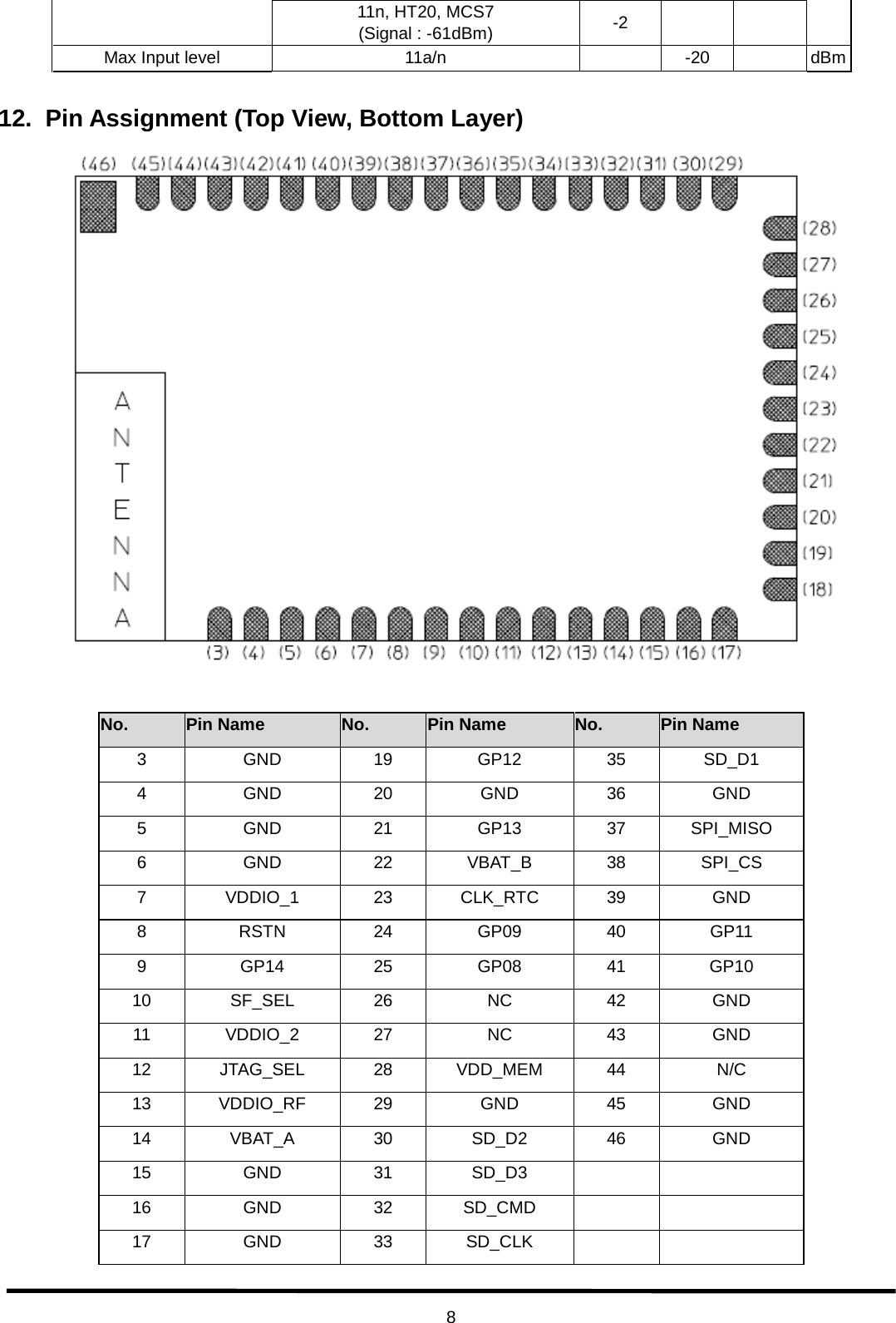
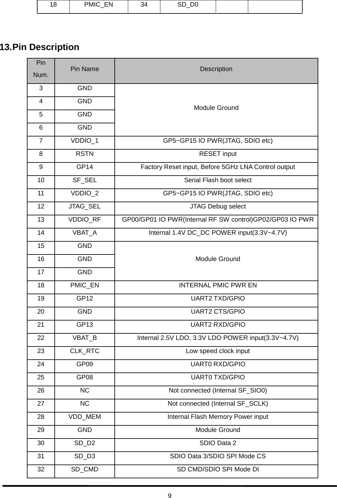
EVERINT WD-MSO WLAN Module User Manual
EVERINT Co.,Ltd. WLAN Module Users Manual
UserManual.wiki
>
EVERINT
>
WD MSO User Manual
Users Manual
Navigation menu
Upload a User Manual
Namespaces
Wiki Guide
HTML
PDF
Info
Views
User Manual
Discussion / Help
Navigation
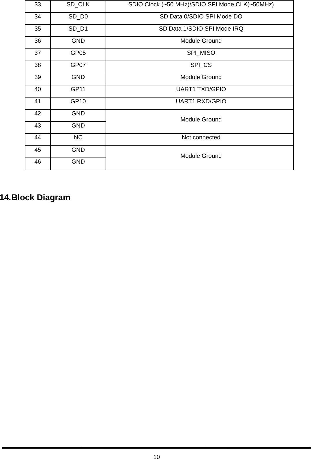
![11 Figure 3. Block Diagram 15. Power Sequence ※ When VCC is below 3.0V, it must be reset. 2.4/5GChip AVDDIO_RF GPIO/UART SDIO/SPI CLK_RTC VDD_MEM VBAT Rx control WF5000 Wi-Fi Chip 2.4GHz Switch Ref CLK (40MHz) Serial Flash (32Mbit) control Shield CAN VDDIO Tx Rx Tx 5GHz FEM DIPLEXER VDD_FEM VBAT_3.3[V]~4.7[V] PMIC_EN RESET Min 10uS Min 10mS Power down VDDIO_3.3[V] SF_SEL Min 10uS](https://usermanual.wiki/EVERINT/WD-MSO/User-Guide-3279831-Page-11.png)