Ingenu NODE102 Wireless network module User Manual microNode Integration Specification

On-Ramp Wireless Wireless network module microNode Integration Specification
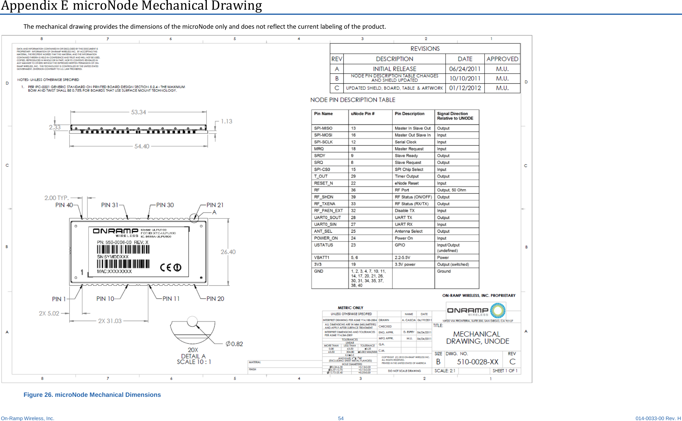
User Manual

            TOTAL REACH NETWORK On-Ramp Wireless Confidential and Proprietary. This document is not to be used, disclosed, or distributed to anyone without express written consent from On-Ramp Wireless, Inc. The recipient of this document shall respect the security of this document and maintain the confidentiality of the information it contains. The master copy of this document is stored in electronic format, therefore any hard or soft copy used for distribution purposes must be considered as uncontrolled. Reference should be made to On-Ramp Wireless, Inc. to obtain the latest revision. microNode Integration Specification
  On-Ramp Wireless, Inc. 10920 Via Frontera, Suite 200 San Diego, CA 92127 U.S.A.  Copyright © 2015 On-Ramp Wireless, Inc. All Rights Reserved.  The information disclosed in this document is proprietary to On-Ramp Wireless, Inc. and is not to be used or disclosed to unauthorized persons without the written consent of On-Ramp Wireless, Inc. The recipient of this document shall respect the security of this document and maintain the confidentiality of the information it contains. The master copy of this document is stored in electronic format, therefore any hard or soft copy used for distribution purposes must be considered as uncontrolled.  Reference should be made to On-Ramp Wireless, Inc. to obtain the latest version. By accepting this material the recipient agrees that this material and the information contained therein is to be held in confidence and in trust and will not be used, copied, reproduced in whole or in part, nor its contents revealed in any manner to others without the express written permission of On-Ramp Wireless, Inc. On-Ramp Wireless, Inc. reserves the right to make changes to the product(s) or information contained herein without notice. No liability is assumed for any damages arising directly or indirectly by their use or application. The information provided in this document is provided on an “as is” basis.  This document contains On-Ramp Wireless, Inc. proprietary information and must be shredded when discarded. This documentation and the software described in it are copyrighted with all rights reserved. This documentation and the software may not be copied, except as otherwise provided in your software license or as expressly permitted in writing by On-Ramp Wireless, Inc. Any sample code herein is provided for your convenience and has not been tested or designed to work on any particular system configuration. It is provided “AS IS” and your use of this sample code, whether as provided or with any modification, is at your own risk. On-Ramp Wireless, Inc. undertakes no liability or responsibility with respect to the sample code, and disclaims all warranties, express and implied, including without limitation warranties on merchantability, fitness for a specified purpose, and infringement. On-Ramp Wireless, Inc. reserves all rights in the sample code, and permits use of this sample code only for educational and reference purposes. This technology and technical data may be subject to U.S. and international export, re-export or transfer (“export”) laws. Diversion contrary to U.S. and international law is strictly prohibited. RPMA® (Random Phase Multiple Access) is a registered trademark of On-Ramp Wireless, Inc. Other product and brand names may be trademarks or registered trademarks of their respective owners.  microNode Integration Specification 014-0033-00 Rev. H April 8, 2015
 On-Ramp Wireless, Inc. iii 014-0033-00 Rev. H Contents 1 Overview ................................................................................................................ 1 1.1 On-Ramp Total Reach Wireless Network .................................................................................. 1 1.2 microNode .................................................................................................................................. 2 1.3 Referenced Documents ............................................................................................................. 3 2 DC and AC Characteristics .................................................................................. 4 2.1 Absolute Maximum Ratings ....................................................................................................... 4 2.2 Recommended Operating Conditions ........................................................................................ 4 2.3 Effects of Temperature and Voltage .......................................................................................... 6 3 Electrical Interface .............................................................................................. 10 3.1 Signal Descriptions .................................................................................................................. 12 3.1.1 VBATT ............................................................................................................................ 12 3.1.2 POWER_ON ................................................................................................................... 12 3.1.3 RESET_N ....................................................................................................................... 12 3.1.4 MRQ ............................................................................................................................... 13 3.1.5 SRDY .............................................................................................................................. 13 3.1.6 SRQ ................................................................................................................................ 13 3.1.7 USTATUS ....................................................................................................................... 13 3.1.8 SPI System ..................................................................................................................... 13 3.1.9 ANT_SEL ........................................................................................................................ 13 3.1.10 UART_SIN .................................................................................................................... 13 3.1.11 UART_SOUT ................................................................................................................ 13 3.1.12 TOUT ............................................................................................................................ 14 3.1.13 RF_PAEN_EXT ............................................................................................................ 14 3.1.14 RF_TXENA ................................................................................................................... 14 3.1.15 RF_SHDN ..................................................................................................................... 14 3.1.16 RF ................................................................................................................................. 14 3.2 Environmental .......................................................................................................................... 14 3.2.1 ESD ................................................................................................................................ 14 3.2.2 Harsh Environments ....................................................................................................... 15 4 SPI Interface and Sequences ............................................................................. 16 4.1 SPI System Interface Overview ............................................................................................... 16 4.2 SPI Mode and Timing............................................................................................................... 17 4.3 Host Initialization ...................................................................................................................... 17 4.4 Startup (Power On) Sequence ................................................................................................. 17 4.5 Wake Sequence ....................................................................................................................... 19
microNode Integration Specification Contents On-Ramp Wireless, Inc. iv 014-0033-00 Rev. H 4.5.1 Wake Sequence (Synchronous) ..................................................................................... 19 4.5.2 Wake Sequence (Asynchronous) ................................................................................... 20 4.6 Host-Driven Reset Sequence .................................................................................................. 21 4.7 Host MRQ Release/microNode Allowed to Sleep Sequence .................................................. 22 5 Power States ....................................................................................................... 23 5.1 Operating States ...................................................................................................................... 23 5.1.1 Power Off State .............................................................................................................. 23 5.1.2 Deep Sleep State ........................................................................................................... 24 5.1.3 Oscillator Calibration State ............................................................................................. 24 5.1.4 Idle State ........................................................................................................................ 25 5.1.5 RX State ......................................................................................................................... 25 5.1.6 TX State .......................................................................................................................... 25 5.2 System ..................................................................................................................................... 25 6 Messaging Protocol ............................................................................................ 27 6.1 Arbitration ................................................................................................................................. 27 6.2 Message Protocol .................................................................................................................... 27 6.3 Host Interface SPI Bus State Machine..................................................................................... 30 6.4 SPI Bus Timing Example ......................................................................................................... 31 6.5 Host Message SPI Example .................................................................................................... 32 6.6 Host Message “Connect” SPI Example ................................................................................... 34 7 microNode Provisioning .................................................................................... 37 8 Antenna Diversity ............................................................................................... 38 8.1 Antenna Design Considerations .............................................................................................. 39 8.2 Diversity Considerations .......................................................................................................... 39 9 Regulatory Considerations ................................................................................ 40 9.1 Block Diagram .......................................................................................................................... 40 9.2 Antennas .................................................................................................................................. 41 9.3 Certifications ............................................................................................................................ 42 9.4 FCC Warnings .......................................................................................................................... 43 9.5 IC Warnings ............................................................................................................................. 43 9.6 ETSI Warnings ......................................................................................................................... 44 9.7 Usage ....................................................................................................................................... 44 9.7.1 Product Labels ................................................................................................................ 44 9.7.2 RF Exposure Statement ................................................................................................. 45 9.8 WEEE Directive ........................................................................................................................ 45 9.9 REACH Directive ...................................................................................................................... 45 9.10 RoHS Directive ....................................................................................................................... 46 9.11 Export Compliance ................................................................................................................. 46
microNode Integration Specification Contents On-Ramp Wireless, Inc.  v  014-0033-00 Rev. H 10 Manufacturing Considerations ........................................................................ 47 10.1 Mechanical Outline................................................................................................................. 47 10.2 Host PCB Constraints ............................................................................................................ 47 10.3 Handling Procedures for microNode ...................................................................................... 47 11 Errata ................................................................................................................. 48 Appendix A Abbreviations and Terms ................................................................. 49 Appendix B PCB Land Pattern and Vias .............................................................. 51 Appendix C REACH AND RoHS Compliance....................................................... 52 Appendix D On-Ramp Wireless RMA Process .................................................... 53 Appendix E microNode Mechanical Drawing ...................................................... 54  Figures Figure 1. On-Ramp Total Reach Wireless Network ......................................................................... 1 Figure 2. microNode (Top and Bottom Views) ................................................................................. 2 Figure 3. Typical Application Diagram ............................................................................................. 3 Figure 4. microNode Deep Sleep Power Consumption (mW Power vs VBATT Input) ................... 7 Figure 5. RX State Power Consumption (mW Power vs VBATT Input) .......................................... 8 Figure 6. microNode1: TX Power Consumption at 20.8 dBm (mW Power vs VBATT Input) .......... 8 Figure 7. microNode2: TX Power Consumption at 23.3 dBm (Watts Power vs VBATT Input) .......................................................................................................................................... 9 Figure 8. SPI Timing, CPOL = 0, CPHA = 0 .................................................................................. 17 Figure 9. microNode Power-up Timing Sequence ......................................................................... 18 Figure 10. Host-Initiated microNode Wake Sequence – SRDY Low (Synchronous) .................... 19 Figure 11. Host-Initiated microNode Wake Sequence – SRDY High (Asynchronous) .................. 20 Figure 12. Host-Driven Reset Sequence ....................................................................................... 21 Figure 13. Host MRQ Release/microNode Allowed to Sleep Sequence ....................................... 22 Figure 14. microNode Oscillator Calibration: Current (Amps) vs Time (Seconds) ........................ 24 Figure 15. Representative Current Consumption During Deep Sleep, Idle, RX, and TX; x16 Spreading Factor (Amps vs Seconds) .............................................................................. 26 Figure 16. SPI Master and Slave Message Sequences ................................................................ 29 Figure 17. Host Interface SPI Bus State Machine ......................................................................... 30 Figure 18. SPI Timing Example ..................................................................................................... 31 Figure 19. Host Message on SPI – MMsg Pair .............................................................................. 32
microNode Integration Specification Contents On-Ramp Wireless, Inc. vi 014-0033-00 Rev. H Figure 20. Host Message on SPI – MHdr Pair ............................................................................... 33 Figure 21. Antenna Diversity Circuit .............................................................................................. 38 Figure 22. microNode Block Diagram ............................................................................................ 41 Figure 23. Product Label ................................................................................................................ 45 Figure 24. microNode PCB Land Pattern ...................................................................................... 51 Figure 25. microNode/Host Vias .................................................................................................... 51 Figure 26. microNode Mechanical Dimensions ............................................................................. 54  Tables Table 1. microNode Version Comparison ........................................................................................ 2 Table 2. Absolute Maximum Ratings ............................................................................................... 4 Table 3. Operating Conditions ......................................................................................................... 4 Table 4. Operating Characteristics .................................................................................................. 4 Table 5. microNode Pin Descriptions ............................................................................................. 10 Table 6. ESD Information ............................................................................................................... 14 Table 7. microNode1: On-Ramp Wireless EMC Certified Antennas ............................................. 41 Table 8. microNode2: On-Ramp Wireless EMC Certified Antenna ............................................... 42 Table 9. microNode Certifications .................................................................................................. 42 Table 10. RF Certification IDs ........................................................................................................ 44 Table 11. Label Statements ........................................................................................................... 45 Table 12. ECCN and CCATS Information...................................................................................... 46
 On-Ramp Wireless, Inc. vii 014-0033-00 Rev. H Revision History Revision Release Date Change Description A  January 18, 2012 Initial release. B  March 13, 2012  Expanded information for regulatory considerations and certifications.  Removed errata section that is no longer relevant. C  May 24, 2012  Updated DC and AC characteristics.  Added new antenna information to the certification chapter. D  July 11, 2012 Updated the Maximum RF Conducted Power. E  September 14, 2012 Added more detail about the microNode in the Overview chapter. Updated notes below the Operating Characteristics table relating to transmit power configuration during provisioning. F  May 13, 2014  Clarified Absolute Maximum Ratings (Input Voltage), pin and signal descriptions, SPI Interface overview, configuration information, antenna diversity information, and manufacturing considerations.  Updated regulatory information and added conformance and compliance information.  Added appendices for: − On-Ramp Wireless RMA information. − microNode Tray mechanical drawing  Updated document references.  Updated to current publishing standards. G  September 29, 2014 Updated manufacturing considerations and recommendations for cleaning the microNode. H  April 8, 2015  Updated for microNode2 and MTBF.  Updated appendices for regulatory and manufacturing considerations.
 On-Ramp Wireless, Inc.  1  014-0033-00 Rev. H 1 Overview This document provides a brief overview of the On-Ramp Total Reach wireless network as well as guidelines allowing an integrator to design a Host product that utilizes the microNode and ensures that the system meets all of its technical objectives and requirements. 1.1 On-Ramp Total Reach Wireless Network The On-Ramp Total Reach wireless network is comprised of microNodes and Access Points (AP). The microNode is designed to easily integrate, through standard interfaces, with sensors enabling robust wireless communication with one or more Access Points interfaced with a customer’s local or wide area network.    Figure 1. On-Ramp Total Reach Wireless Network
microNode Integration Specification Overview On-Ramp Wireless, Inc.  2  014-0033-00 Rev. H 1.2 microNode The microNode is a small form factor wireless network module that easily integrates with various devices and sensors using an industry standard Serial Peripheral Interface (SPI). There are two versions of the microNode. The primary difference between the two versions of the microNode is transmit power. The following table summarizes the differences and recommendations. Table 1. microNode Version Comparison Version Transmit Power  Benefits  Comments microNode1 (PN 550-0006-00) +20.8 dBm (max)    This is the first version of the microNode and is not recommended for new designs. microNode2 (PN 550-0075-00) +23.3 dBm (max)  More power efficient for its transmitter functions  More liberal on its FCC allowances This is the second version of microNode and is the recommended version for new designs.  NOTE: This document refers to both microNode1 and microNode2 generically as “microNode.” Where there are differences, the microNode version is specified (i.e., microNode1 or microNode2). The top side of the printed circuit board (PCB) is enclosed with a radio frequency (RF) shield. The microNode is soldered directly onto a host board via SMT processes. For details, see Appendix B. Dimensions (per unit):  54.40 mm long by 26.40 mm wide Weight (per unit):  0.30 oz (8.5 g) For more details about the microNode, refer to the mechanical drawing in Appendix E.  To order, use the part numbers provided in Table 1.  Figure 2. microNode (Top and Bottom Views)
microNode Integration Specification Overview On-Ramp Wireless, Inc.  3  014-0033-00 Rev. H The following figure shows how a microNode interfaces with a Host application.  Figure 3. Typical Application Diagram 1.3 Referenced Documents The following documents are referenced and provide more detail.  EMC Compliance Guide (010-0037-00) Provides information for “driving” the Node through various modes in order to perform regulatory tests for FCC and ETSI.  ATE Transmit Test Mode Guide (010-0089-00) This guide provides commands for factory testing the device’s transmitter and antenna ports.  Provisioning Guide (010-0074-00)  Describes the function and use of the software packages used to configure a node for a particular application and target network.  RMA Request Form (007-0003-00) This is the form to use for returning material/product to On-Ramp Wireless for repair and/or replacement.  microNode Label Specification (014-0031-00) This document specifies  label and revision information for the microNode.  rACM Developer Guide (010-0105-00) Describes the necessary steps to build, download, and test the reference Application Communication Module (rACM) software. It is used by external partners in the development of a sensor application on the reference host platform using On-Ramp Total Reach wireless technology.  The rACM software serves as a design template and is optimized for very low power usage applications and battery-powered systems.  Host Common Software Integration Application Note (010-0024-00) Describes the software interfaces and implementation considerations regarding the On-Ramp Wireless Total Reach Host Common software component – a library of portable C code which facilitates all interactions between a host application and an On-Ramp Wireless Total Reach Network node.
 On-Ramp Wireless, Inc.  4  014-0033-00 Rev. H 2 DC and AC Characteristics 2.1 Absolute Maximum Ratings Operating outside of these ranges may damage the unit. The microNode is MSL 3-rated and should be handled as an MSL 3 device per IPC/JEDEC J-STD-033 (latest revision). See section 10.3 for further information. Table 2. Absolute Maximum Ratings Parameter Min Max Unit Storage Temperature  -40 85 ⁰C Operating Temperature  -40 85 ⁰C Input Voltage 2.2 6.0  V 3 Digital Interface Signals, 3.3V nominal    3.6  V 2.2 Recommended Operating Conditions Table 3. Operating Conditions Parameter Min Max Unit Input voltage, VBATT 2.2 5.5  V Ambient Temperature, Ta  -40 85 ⁰C  The following characteristics apply across the -40°C to +85°C temperature range unless otherwise noted. Table 4. Operating Characteristics Description Min Typ Max Units DC Characteristics Voltage – VBATT  2.2 3.6 5.5  Volt Off Current – Note 1 0.05 0.1 2.0  µA Deep Sleep Current - Note 1 10 20 40 µA Idle Current – Note 1 10 15 25 mA Receive Current – Note 1 75 85 90 mA microNode1: Transmit Current – Note 2 200 245 280 mA microNode2: Transmit Current – Note 2 220 250 280 mA Digital VOL – Voltage Output, Low (4mA sink)  0    0.1  V VOH – Voltage Output High (4mA source)   2.4    3.2  V SPI Clock – Note 11 0.1    8.6 MHz
microNode Integration Specification DC and AC Characteristics On-Ramp Wireless, Inc.  5  014-0033-00 Rev. H Description Min Typ Max Units Environmental Operating Temperature  -40    +85 °C Storage Temp  -40    +85 °C Humidity – non-condensing  5    95  % Ramp Temperature (maximum rate at which operating temperature should change)     30 °C/Hr. MTBF (microNode1)    10.5     MHrs MTBF (microNode2)    6.4    MHrs Receiver Receiver Sensitivity – Note 3  -130  -133  -135  dBm Receiver Image Reject 38 45 50 dB Noise Figure  3.5 5.0 6.7 dB Input IP3 (high LNA gain mode)    -11    dBm Maximum RF input level for specification compliance      -20  dBm General RF Characteristics Frequency Range – Note 4 2402    ~2482 MHz Channel Spacing  N/A 1.99 N/A MHz Transmitter Maximum RF Conducted Power –Note 5 FCC/IC markets: ETSI markets:  20.0 8.5  20.4 9.5  20.8 10.0  dBm dBm Carrier Rejection  -35  -40  -50  dBc Signal Modulation     DSSS- DBPSK     Signal Bandwidth    1.0    MHz BT Factor    0.3     Peak to Average Ratio    2.3    dB Spectral bandwidth at maximum RF power: -6dB BW -20dB BW    0.96 1.75    MHz MHz ACPR – Note 6      -30  dBc Harmonics – Note 7      -43  dBm Transmit Power Level Accuracy – Note 8      ±1.5 dB Transmitter Spurious Outputs – Note 9     30MHz to 2400MHz:     2482MHz to 8000MHz:      < -43 < -43  dBm dBm VSWR Tolerance   Maximum VSWR for spec compliance – Note 10:   Maximum VSWR for stability.      1.5:1 9:1   NOTES: 1. Tested at 3.6V input, +25C. Please note the following:
microNode Integration Specification DC and AC Characteristics On-Ramp Wireless, Inc.  6  014-0033-00 Rev. H a. There are power differences between the Voltage/Current numbers in this table and the data provided in Figure 4, Figure 5, and Figure 6. These figures show representative characterization of Power over Voltage/Temperature characterization and are only representative behavior. b. The Table 4 refers to a maximal current draw that the Host system should be designed to accommodate. 2. Measured at:  microNode1:  +20.8 dBm TX output (Typ=50Ω), 3.6V, range includes VSWR ≤ 1.5:1 (Po not compensated).  microNode2:  +23.3dBm TX output (Typ=50Ω), 3.6V, range includes VSWR ≤ 1.5:1 (Po not compensated). 3. Sensitivity at maximum spreading factor of 13 (2048) with 10% FER. 4. The upper frequency range is market dependent: a. FCC/IC: CH38; 2475.63 MHz. b. ETSI: CH40; 2479.61 MHz. c. Japan: CH41; 2481.60 MHz. 5. Maximum TX RF power:  microNode1: This is limited by FCC/IC grant to 20.8 dBm in these markets. Transmit power is configured during the provisioning process to meet country-specific deployment and regulatory requirements. The configurable range is 0 – 20.8 dBm.  microNode2: This is limited by FCC/IC grant to 23.3 dBm in these markets. Transmit power is configured during the provisioning process to meet country-specific deployment and regulatory requirements. The configurable range is 0 – 20.8 dBm. 6. Spec and test method comes from FCC 15.247(d); Band Edge Emissions, 2 MHz offset. 7. At any TX power level, VSWR ≤ 3:1. Harmonics fall into FCC restricted bands. 8. Estimated sum of all contributors with VSWR ≤ 1.5:1. Normal link mode. 9. At any TX power level, VSWR ≤ 3:1. Applies to spurious, not ACPR or harmonics. Generally the largest spurious output outside the 2.40-2.48GHz band is at 2/3LO and 4/3LO. 10. Maximum VSWR for spec compliance applies at 25°C only. Slightly degraded ACPR/mask and power variation can be expected at temperature extremes. 11. The SPI clock has a maximum rate of 26 MHz/3 and a minimum of 100 kHz. There is no physical limitation on the minimum clock rate but the 100 kHz is deemed “marginal” and is not absolute. Depending on the data traffic model and level of debug traffic, 100 kHz may cause a backup of SPI traffic, which then causes buffer overflow conditions.  The application must be validated to ensure that the SPI clock is sufficient to support required traffic. 2.3 Effects of Temperature and Voltage The microNode is based largely on Complementary Metal–Oxide–Semiconductor (CMOS) technology. The current drain of CMOS circuitry can vary substantially over Temperature. The RF circuitry and its performance also vary substantially over Temperature.  The microNode utilizes two main power domains when it is functioning:
microNode Integration Specification DC and AC Characteristics On-Ramp Wireless, Inc.  7  014-0033-00 Rev. H 1. LDO Regulators that work from 2.2V up to 5.5V.  These are enabled when the POWER_ON signal for the microNode is active. These can act as a linear load as voltage increases from minimum to maximum – although these circuits do not normally consume much power. 2. Switching power domains.  When the microNode wakes up to communicate with the Host or for networking events, its switching regulators are enabled. These buck-boost switching regulators supply the 3.3V and other logic supplies over the input range of 2.2-5.5V. The power efficiency of these regulators change dramatically over input voltage, load levels, and temperature. Nominally, the power efficiency is best at 3-4.0V. The efficiency becomes poor below 3.0V and is moderately efficient at the higher input levels. The following graphs show the relative differences across the operating voltages and their effect on current consumption.    Figure 4. microNode Deep Sleep Power Consumption (mW Power vs VBATT Input)  00.050.10.150.20.2522.5 33.5 44.5 55.5-40C Sleep-30C Sleep-20C Sleep-10C Sleep0C Sleep10C Sleep20C Sleep30C Sleep40C Sleep50C Sleep60C Sleep70C Sleep
microNode Integration Specification DC and AC Characteristics On-Ramp Wireless, Inc.  8  014-0033-00 Rev. H  Figure 5. RX State Power Consumption (mW Power vs VBATT Input)   Figure 6. microNode1: TX Power Consumption at 20.8 dBm (mW Power vs VBATT Input) 30031032033034035036037038022.5 33.5 44.5 55.5-40C RX-30C RX-20C RX-10C RX0C RX10C RX20C RX30C RX40C RX50C RX60C RX70C RX8909109309509709901010103022.5 33.5 44.5 55.5-40C TX max-30C TX max-20C TX max-10C TX max0C TX max10C TX max20C TX max30C TX max40C TX max50C TX max60C TX max70C TX max80C TX max85C TX max
microNode Integration Specification DC and AC Characteristics On-Ramp Wireless, Inc.  9  014-0033-00 Rev. H  Figure 7. microNode2: TX Power Consumption at 23.3 dBm (Watts Power vs VBATT Input)  0.60.650.70.750.80.850.90.9511.051.11.5 2.5 3.5 4.5 5.5 6.5-40C-20C0+25C+50C+85C
 On-Ramp Wireless, Inc. 10 014-0033-00 Rev. H 3 Electrical Interface This chapter describes the electrical interface of the microNode and how the Host processor controls the microNode. Table 5. microNode Pin Descriptions Pin # Pin Name Signal Direction Relative to microNode Signal Type Comment 1, 2, 3, 4, 7, 10 Ground Power Power Ground return. Should be low RF impedance to a solid ground plane of the Host 11,14, 17, 20, 21, 26, 30, 31, 34, 35, 37, 38, 40 Ground Power Power    5, 6  VBATT  Power Power Input power to the microNode. It is recommended that the Host integrator allow for decoupling of the microNode by placing space for up to a 100 µF (47 µF nominal) ceramic capacitor. Bypass with an additional 0.1 µF capacitor. This may or may not be required, depending on the Host's power supply and its impedance. 8  SRQ Output CMOS_O Slave Request 9  SRDY Output CMOS_O Slave Ready 12  SCLK Input CMOS_I SPI Clock 13 MISO Output CMOS_O  SPI Master Input Slave Output 15 CS Input CMOS_I SPI Chip Select 16 MOSI Input CMOS_I  SPI Master Output Slave Input 18 MRQ Input CMOS_I Master Request 19  3V3  Output CMOS_O 3.3V Switcher output from the Node 22  RESET_N  Input OC_1 RESET input 23 USTATUS I/O CMOS_O, CMOS_I USTATUS. To be used by the microNode as a GPIO. Undefined at this time. Float for now. 24  POWER_ON  Input CMOS_A This is used to turn ON/OFF the Internal Power supplies of the microNode. 25  ANT_SEL  Output CMOS_O This is used by the microNode to control its antennas for diversity.  27 UART_SIN Input CMOS_I UART Serial input. Not supported at this time.
microNode Integration Specification Electrical Interface On-Ramp Wireless, Inc. 11 014-0033-00 Rev. H Pin # Pin Name Signal Direction Relative to microNode Signal Type Comment 28 UART_SOUT Output CMOS_O UART Serial output. Not supported at this time. 29  TOUT Output CMOS_O TOUT is a normally low signal that pulses high in response to specific Network Timing Events 32  RF_PAEN_EXT  Input CMOS_I This is used to force the PA off. It is internally pulled low. Do not connect at this time. 33 RF_TXENA Output CMOS_O This signal is used to indicate status of the Power Amplifier for the microNode: Low = OFF, High = Enabled (Transmitting). 36 RF RF RX/TX 50 Ohm This is the RF input/output for the microNode. It is a 50 Ohm castellated “pin.” 39 RF_SHDN RF Shutdown CMOS_O This pin indicates the status of the RF Transceiver for the microNode: Low= Shutdown, High = Active  NOTES: 1. The VDD of the internal logic of the microNode is 3.3Volt. 2. The Host is the SPI Master and the microNode is the SPI Slave. 3. OC_1 The pin-type is unique for the RESET line. Internal to the microNode, this is a simple RC circuit that Resets to GND (0 Volts) and rises to 1.8Volts (maximum). Externally, it is required to drive this pin via an Open Collector/Drain (States:  Ground = microNode Reset, or float = microNode Active). Most Host CPUs have programmable I/Os that allow setting as an output (low) and as input (tri-state or float). A pull-up is not permitted. Voltages above 1.8V can damage the Reset line of the microNode or place the microNode in a latchup state. 4. CMOS_A   a. The CMOS_A pin is used to control two Analog Regulators and their Enable pins.  b. The pin has hysteresis.  Going High (Active):  V input High is 1.2V  Going Low (OFF):  V input Low is 0.4V c. When the microNode is ON, this pin consumes a nominal 0.2 µA but as maximum of 2 µA over the entire temperature range.
microNode Integration Specification Electrical Interface On-Ramp Wireless, Inc. 12 014-0033-00 Rev. H 5. VBATT a. The microNode operating voltage is 2.2V - 5.5V, which drives a buck/boost regulator (3.3V) internal to the microNode. b. The internal 3.3V regulator drives the RF and PA circuitry of the microNode which also drives its operating CMOS I/O voltages. 6. CMOS_I The Node input voltages are 3.3V CMOS levels. VIH = 2.0V (minimum) and VIL = 0.8V (maximum). 7. CMOS_O The Node output voltages are 3.3V CMOS levels (4mA). VOH = 2.4V (minimum) and VOL = 0.4V (maximum). 8. SPI inputs to the node (SCLK, MOSI, CS) must be tri-stated or driven low when the node may be sleeping (MRQ and SRQ are both low). See section 4: SPI Interface and Sequences for more details. 3.1 Signal Descriptions 3.1.1 VBATT This is the main power to the microNode. This needs a low impedance source to the Host’s power source. It is recommended that the Host have provision for up to a 100 µF (47 µF nominal) low ESR capacitor. Use an additional 0.1 µF capacitor to bypass the large bulk capacitor.  These capacitors help shunt high frequency noise (0.1 µF) and aid in smoothing surge currents as the Node turns itself ON/OFF during normal operations. 3.1.2 POWER_ON This signal controls the power-on of the LDO circuitry for the microNode. It must be shut off prior to starting the microNode power-up sequence as defined in section 4.4: Startup (Power On) Sequence. After the microNode is powered up, this signal is to remain logic high during normal operational modes. 3.1.3 RESET_N The microNode has a basic RC Reset circuit that should be cleared during the startup sequence for the microNode. This signal is an Open Collector/Drain style of signal that can be cleared (grounded) for Reset and allowed to float when the microNode is operational.  CAUTION: This pin should never be exposed to a voltage greater than 1.8V. Signals greater than 1.8 V could damage the Node.
microNode Integration Specification Electrical Interface On-Ramp Wireless, Inc. 13 014-0033-00 Rev. H 3.1.4 MRQ The MRQ (Master Request) is the Host’s normal way of waking the microNode to initiate SPI communications. Logic “High” forces the microNode awake. 3.1.5 SRDY SRDY (Slave Ready) is an indication from the microNode that it has fully booted its internal Firmware image, initialized its Hardware and Interfaces, and is ready for communication (arbitration) with the Host. Logic “High” indicates the microNode is ready for communications. 3.1.6 SRQ The SRQ (Slave Request) signal is an indication from the microNode that it wants the Host’s attention. When SRQ is asserted “High,” the Host must read the Status registers of microNode. If SRQ is “High,” SRDY will also be “High.” 3.1.7 USTATUS USTATUS is currently undefined. In software it can be either an Input or Output. Currently it is configured as an input. The Host should not use this signal. 3.1.8 SPI System The SPI system is the generic term used for all SPI signals (MOSI, MISO, CS, SCLK) to be set up for SPI communications to occur between Host and microNode. The microNode SPI is the Slave in the Master/Slave communications and is defined in section 4.2: SPI Mode and Timing. 3.1.9 ANT_SEL The Antenna Select (microNode output) signal is used to control a RF T/R signal to allow Antenna Diversity. This is more fully defined in Chapter 8: Antenna Diversity. 3.1.10 UART_SIN This UART_SIN is a microNode UART input signal. It is reserved for future use and should not be used by the Host. Leave unconnected. 3.1.11 UART_SOUT The UART_SOUT is a UART output signal that is currently reserved. The Host should not use this pin.
microNode Integration Specification Electrical Interface On-Ramp Wireless, Inc. 14 014-0033-00 Rev. H 3.1.12 TOUT This signal is a Time Synchronizing signal that pulses high upon specific network timing events. 3.1.13 RF_PAEN_EXT The RF_PAEN_EXT signal is a direct hardware signal that can be used to disable the Power Amplifier (PA) for the microNode. This signal is pulled low (100k to ground) to allow the PA to work as normal. A microNode external device can temporarily assert this signal high to de-key the PA for the microNode. The purpose of this direct control is to allow simple coexistence algorithms with other RF devices. If the external device is transmitting, its transmitter signal can disable the PA for the microNode thus avoiding a TX collision. 3.1.14 RF_TXENA This signal is a status output of the microNode that allows other RF devices to monitor when the microNode is transmitting. In a simple RF coexistence scheme, the RF_TXENA can disable a coexisting radio’s transmitter, while the microNode is transmitting. The RF_TXENA signal goes active high when transmitting. 3.1.15 RF_SHDN This microNode output indicates status of the RF Transceiver of the microNode. If low, the transceiver sleeps (no RX and no TX). Using RF_SHDN and RF_TXENA in combination, co-existing RF devices can determine the absolute state of the RF Transceiver of the microNode. 3.1.16 RF This is the RF port (TX and RX) for the microNode. It is a nominal 50 Ohm port. For best results ensure the load termination (antenna) has a VSWR of 1.5:1 or better (return loss < -10 dB). 3.2 Environmental 3.2.1 ESD The microNode is designed to be a truly embedded module and can almost be considered an IC. The microNode is to be placed as a direct-connect to the Host CPU. Therefore, the microNode has inherent minimal electrostatic discharge (ESD) protection on its I/O.  Table 6. ESD Information ESD Model Class and Minimum Voltage HBM Class 1C ( >1000V) MM Class A (>100V)
microNode Integration Specification Electrical Interface On-Ramp Wireless, Inc. 15 014-0033-00 Rev. H The RF port does have some protection in the form of an inductor to ground, thus allowing some robustness to direct ESD strikes.  If the application is intended for harsh ESD or lightning strike scenarios it is recommended that the Integrator take extra precautions to guard against accidental resets or ESD damage. 3.2.2 Harsh Environments The microNode employs miniature surface-mounted components in its assembly. If the target design is intended for high humidity or salt environments and intended to have a long service life, it is recommended that the designer take necessary precautions to guard against prolonged exposure to moisture and other contaminants. A sealed enclosure (IP67 or IP68) or potting may be required in extreme environments.
 On-Ramp Wireless, Inc. 16 014-0033-00 Rev. H 4 SPI Interface and Sequences 4.1 SPI System Interface Overview The SPI slave interface is currently the only supported interface for Host-to-Node communication. NOTE: The microNode must be the only SPI slave on the bus.  The SPI slave interface provides communication with an external Host through a 7-wire interface. The Host is the SPI master and the microNode is the SPI slave. In addition to the four standard SPI signals, three additional signals are used to complement the SPI bus: MRQ, SRQ, and SRDY. The additional signals are included to support microNode state transitions and bi-directional message traffic. The SPI signals include four that are controlled by the master and three that are controlled by the slave. Master-controlled Signals (Host)  MOSI  SCLK  CS  MRQ Slave-controlled Signals (microNode)  MISO  SRQ  SRDY When MRQ and SRQ are low, the remaining Master controlled signals (MOSI, SCLK, and CS) must be held low or tri-stated. This is to prevent these signals from back-driving the microNode (Slave) that may be in deep sleep. When either MRQ or SRQ assert high, the Master should set each of the three signals appropriately according to their standard usage. No pull-up resistors should ever be applied to any signals on the microNode since it often needs to fall into a Deep Sleep mode (all internal regulators turned off).
microNode Integration Specification SPI Interface and Sequences On-Ramp Wireless, Inc. 17 014-0033-00 Rev. H 4.2 SPI Mode and Timing  MOSI(from master)1NSS(to slave)MISO(from slave)SPCK(CPOL = 0)2 3 4 5 6 7 8SPCK Cycle (for reference)MSBMSBLSBLSB *6 5 4 3 2 16 5 4 3 2 1 Figure 8. SPI Timing, CPOL = 0, CPHA = 0 4.3 Host Initialization What is described here is the initialization of the Host, its operating software, and the control sequences used to drive the microNode.  Due to specific clock and memory requirements, the microNode must go through specific Initialization and Wake sequences.  NOTE:  Some CPUs have internal pull-up resistors that are active after Power On Reset. Through CMOS leakage, the Host CPU can supply voltages to the microNode I/O bus prior to the Host CPU fully initializing and disabling the pull-up resistors. It must be noted that during the brief initialization period, the POWER_ON signal must be “low.” Activating the POWER_ON signal with other microNode signals being pulled “high” can cause CMOS latchup within the microNode.  4.4 Startup (Power On) Sequence During, and immediately after Power On Reset (POR), the Host has no control of its I/O power states. For instance, some CPUs have GPIO that tri-state or act as inputs during power up. Other CPU brands have programmable pull-ups on its I/O and need the Host CPU to disable those pull-ups for the Host’s GPIO to work correctly with the microNode. This setup and configuration of GPIO takes a finite time during the Host boot process. This is detailed in the following figure. Whereas the power-up sequence is described here, it is recommended the Integrator not attempt this entire startup sequence without assistance. On-Ramp Wireless offers a formal and controlled library to help with this startup and communication interface. For more information, refer to the rACM Developer Guide (010-0105-00) and the Host Common Software Integration Application Note (010-0024-00). These documents are described in section 1.3: Referenced Documents.
microNode Integration Specification SPI Interface and Sequences On-Ramp Wireless, Inc. 18 014-0033-00 Rev. H  t0t1t2t3t4t5t61000 ms 10 ms 4 mst6 – t4 < 300 ms or errorSRDYSPI SystemMRQReset_NPower OnHost Init(not a signal)VBATTHi-Z100 ms Figure 9. microNode Power-up Timing Sequence  The timing sequence shown in Figure 9 above is described below. NOTE: The timing shown in the figure is not to scale.  t0  t1 This phase is where the Host’s System power has been applied and the Host Software must power up and initialize the GPIO interfaces for the microNode to the required states defined at time t1. The t1 state becomes “TRUE” indicating the Host sets all the GPIO to a known and controlled state (Low).   t2 At t2 state, all the output signals to the microNode are set low and the Power On Signal is set high. This turns on the internal LDO regulators of the microNode to initiate a power up sequence. The time between t1-t2 is approximately 100 ms, or longer.  t3 t3 is when the Host releases the microNode from its Reset state. This time allows the 32 kHz of the microNode to turn on and stabilize. The time between t2-t3 is 1 second, or longer.  t4 t4 signals the start of the Host wanting to initiate communications (arbitration) with the microNode. The Host raises MRQ to turn on various circuitries. The time between t3-t4 is 10 ms, or longer.
microNode Integration Specification SPI Interface and Sequences On-Ramp Wireless, Inc. 19 014-0033-00 Rev. H  t5 After the assertion of t4, the microNode begins its “wake sequence.” The microNode must boot, initialize its operating system and hardware and when it is ready for communications it raises its SRDY signal back to the Host. At this point, communications (Arbitration) can begin.  t6 At this point the microNode signals its readiness by asserting the SRDY pin. The Host can now begin communications with the microNode. 4.5 Wake Sequence  The microNode can be awakened in two manners:   MRQ assertion from the Host. The Host desires communications with the microNode and awakens the microNode by asserting the MRQ line. This is a Synchronous Wake Sequence.  The microNode can “self-awaken” due to network events. In this case, a timer internal to the microNode “pops” and triggers the microNode to “wake.” When the microNode is awake it asserts its SRDY as a matter of course to indicate to the Host (if it needs to) that it can start communicating with the microNode while it is awake. This is an Asynchronous Wake Sequence. 4.5.1 Wake Sequence (Synchronous) The following sequence demonstrates the timing required of the Host to awaken the microNode from a sleep state. Assumptions:  The microNode has been previously Powered On and Arbitrated.  The power (VBATT) has remained stable and the microNode has not been Reset (Reset is set to tri-state/float). t0t1t2t3SRDYSPI SystemMRQHi-Z4 ms(Driven as appropriate)3 ms Figure 10. Host-Initiated microNode Wake Sequence – SRDY Low (Synchronous)
microNode Integration Specification SPI Interface and Sequences On-Ramp Wireless, Inc. 20 014-0033-00 Rev. H The timing sequence shown in Figure 10 above is described below. NOTE: The timing shown in the figure is not to scale.  t0 The Host desires to wake the microNode and asserts MRQ high.  t0  t1 After MRQ has gone High, the Host’s SPI system and other I/O can be enabled. Asserting the MRQ has enabled the internal I/O power supply of the microNode and the Host’s SPI can be enabled 4 ms after the rise of MRQ.  t1  t2 After the initial assertion of MRQ, the microNode has to internally power up and initialize its systems. When it is ready to communicate it will assert its SRDY line to signal it is now ready for SPI interaction. From MRQ assertion until the microNode is ready, takes about 80 ms.  t3 The microNode is now ready to communicate with the Host. 4.5.2 Wake Sequence (Asynchronous) In this scenario, the microNode is already awake due to a networking event (SRDY is already High) and the Host wants to communicate with the microNode while it is awake. The Host asserts MRQ to ensure that the microNode stays awake during its communication cycle. NOTE: The timing shown in the figure is not to scale.  t0t1t2t3SRDYSPI SystemMRQHi-Z (Driven as appropriate)< 250 μs Figure 11. Host-Initiated microNode Wake Sequence – SRDY High (Asynchronous)
microNode Integration Specification SPI Interface and Sequences On-Ramp Wireless, Inc. 21 014-0033-00 Rev. H 4.6 Host-Driven Reset Sequence If the microNode fails to communicate (or similar), it may be necessary to Reset the microNode. The following figure shows the proper sequence to reset the device.  NOTE 1: Resetting the device causes it to go through a Cold Acquisition process to reacquire the network. NOTE 2: The timing shown in the figure is not to scale.   Power Ont0t1t2t3t4t5t61000 ms 10 ms 4 msSRDYSPI SystemMRQReset_NVBATTHi-Z100 ms(Driven as appropriate) Figure 12. Host-Driven Reset Sequence
microNode Integration Specification SPI Interface and Sequences On-Ramp Wireless, Inc. 22 014-0033-00 Rev. H 4.7 Host MRQ Release/microNode Allowed to Sleep Sequence If the Host determines there are no more messages or SPI transactions required, it nominally de-asserts the MRQ to allow the microNode to fall back to Deep Sleep (lowest power mode). The figure below shows how this is sequenced by the Host/microNode. A small delay in de-asserting SRDY is enforced to prevent quick toggling (waking) of the microNode. NOTE: The timing shown in the figure is not to scale.  t0t1t2SRDYSPI SystemMRQHi-Z10 ms3 ms Figure 13. Host MRQ Release/microNode Allowed to Sleep Sequence
 On-Ramp Wireless, Inc. 23 014-0033-00 Rev. H 5 Power States The microNode has a number of states it runs through during its various operating modes. General comments: 1. The microNode accepts a wide input voltage range (2.2-5.5V). 2.  The microNode has low drop out (LDO) regulators that will operate 100% of the time the microNode is powered (POWER_ON signal set high).  3. There are 3.3V/1.2V Buck/Boost Switching regulators that use the wide input range to drive key RF and Digital circuits. The 3.3V regulator is only turned on in certain active operating states of the microNode. The microNode always tries to minimize its power consumption but is largely driven by network operating states and modes of operation. This document does not describe all of the modes in detail but, in general, there are two main operating modes for the microNode:  Continuous Mode  In this mode, the microNode is ON (awake) at least 50% of the time (100% of its RX cycle). The microNode starts up, searches for the network, locks on, and Joins. In this mode, the microNode nominally is either in RX or TX modes (radio is ON and in a high power consumption state), or in an Idle state where the clocks and CPU are ON but the radio is OFF (moderately low power mode). The continuous mode is usually for applications where the Host and microNode are AC-powered and system current consumption is not an issue.  Slotted Mode  This mode has the microNode falling into a Deep Sleep state – the lowest power state of the microNode. In this mode, the microNode is mostly powered down – except for a couple of low power LDO Regulators. The microNode can sleep for hours at a time if the network is configured to allow this. The power states are described in the following sections. 5.1 Operating States This section describes the various operating states within the operational modes. 5.1.1 Power Off State When the microNode is totally non-functional, the Host can set the POWER_ON signal Low to deactivate the circuitry of the microNode. This should NOT be confused with Deep Sleep states where the microNode mostly sleeps yet maintains key network timers to wake up synchronously with network activity. If awakened from the Power Off state, the microNode must go through a very power-hungry search/acquisition algorithm to re-acquire the On-Ramp Total Reach Network.
microNode Integration Specification Power States On-Ramp Wireless, Inc. 24 014-0033-00 Rev. H 5.1.2 Deep Sleep State The microNode shuts off all its power regulators except a couple low quiescent LDO regulators. These regulators keep a minimal amount of circuitry alive for tracking network timers, enable a 32 kHz clock, and some minor interface circuitry. 5.1.3 Oscillator Calibration State When the microNode is in Deep Sleep state, it attempts to maintain accuracy of its low power 32 kHz clock to enable faster network synchronizing when it wakes up. The CPU of the microNode is not activated during this calibration state. The microNode will periodically (and briefly) wake up in a very low power mode to calibrate its 32 kHz clock to its very accurate 26 MHz clock. This is especially important when the temperature varies substantially causing the 32 kHz oscillator to drift. This is illustrated in the following figure. This plot is an example of the microNode performing a self-calibration of its 32 kHz oscillator. The pulses represent the TCXO being turned on periodically to perform the calibration. The microNode wakes itself from Deep Sleep, Calibrates, and then falls back to sleep. Minimal power is consumed during this self-calibration process. As can be seen, the microNode does this approximately every 900 seconds.   Figure 14. microNode Oscillator Calibration: Current (Amps) vs Time (Seconds)
microNode Integration Specification Power States On-Ramp Wireless, Inc. 25 014-0033-00 Rev. H 5.1.4 Idle State Idle state has various sub-states but generally refers to a state where the microNode is “awake” and its system clock is on, the CPU is awake, but the RF is OFF. 5.1.5 RX State The microNode turns on all its clocks, the main CPU and the RF in an RX-only state. The RF transceiver, in RX state, consumes a moderate amount of power. 5.1.6 TX State When the microNode transmits, it uses a variable transmit power that is correlated to its received RSSI. In this state, the microNode is likely at its highest power states, but this is somewhat dependent on RSSI. The worst case state (maximum power) is shown in Figure 15. This is at approximately 20.8 dBm output power. This is the highest power state for the microNode. 5.2 System As noted, the microNode can go through various states of Deep Sleep, Idle, RX, and TX. The plot shown in the following figure provides a representative microNode waking up and going through these states and transitions. All systems are different and current consumption is affected by many factors.  Network coverage. How much TX power does a microNode need to transmit its data?  Temperature range  Operating Voltage  Continuous mode vs Slotted mode: What is the Uplink Interval?  Amount of data in the data model  Quality of Service (QoS) for data delivery All of the factors indicated above must be examined carefully and plotted to understand the end result in current profiles and expected battery life projections.
microNode Integration Specification Power States On-Ramp Wireless, Inc. 26 014-0033-00 Rev. H  Figure 15. Representative Current Consumption During Deep Sleep, Idle, RX, and TX; x16 Spreading Factor (Amps vs Seconds)  The plot shown in the figure above represents the nominal transitions for the microNode from Deep Sleep, Idle, Receive, and Transmit states. In this case, a TX spreading factor of 16 is used. It is important that the Host designer understand the System operating profile, operating voltages, different operating modes of the microNode and the ultimate effect on System power consumption. Of course, this is especially true if a battery powered device is being considered.
 On-Ramp Wireless, Inc. 27 014-0033-00 Rev. H 6 Messaging Protocol The details of Host/Node messaging are typically not necessary for integrators to implement; however, low-level understanding of the SPI protocol used may be critical in resolving Host interface issues. For mid-level details of the messages that may be sent over this interface, refer to Node Host Message Specification (014-0020-00). 6.1 Arbitration Arbitration is the process a Host uses to signal to the Node that it supports the On-Ramp Wireless bi-directional messaging protocol. The arbitration sequence is designed to reduce the probability that an arbitrary non-Host transfer sequence can mirror a valid arbitration sequence. Arbitration consists of both Host and Node transmitting an arbitration request/reply pair. After a defined turn-around delay, both transmit a validation request/reply. The turn-around delay avoids race conditions between Host and Node and provides enough time to allow ISR execution to complete before the next SPI transfer. If the Node does not reply to the Host request, the Host needs to wait for a turn-around delay and retry the arbitration request. The Host must perform the arbitration sequence before any other SPI Bus communication can take place between the Host and the Node. The Host must initiate this arbitration sequence on boot up. Additionally, the Host must perform the arbitration sequence when the Node sends to the Host an arbitration message. This can occur due to the Node going into Deep Sleep and then waking up. Since the Node requires the arbitration sequence after waking from Deep Sleep and since the Host is not aware of when the Node goes to Deep Sleep, the Host must be able to detect that the Node is requesting arbitration and the Host must then reset its Host interface state machine and perform arbitration. For more information on the Host interface SPI bus state machine, refer to section 6.3: Host Interface SPI Bus State Machine. 6.2 Message Protocol Host-to-Node transfers use master message command pairs and Node-to-Host transfers use slave message command pairs. Both transfers use identical command sequences with only the encoding of the commands differing. The command sequence for a message transfer consists of a request/acknowledgement pair followed by a defined turn-around delay and then a message composed of a header pair and a payload. Variable length payloads are supported by encoding the payload size in the second half of the message request. The second half of the message reply contains the available receive buffer size. If the message payload size exceeds the receive buffer size, then a new request must be made after a turn-around delay with a payload size that does not exceed the receive buffer size.
microNode Integration Specification Messaging Protocol On-Ramp Wireless, Inc. 28 014-0033-00 Rev. H After a successful message request transfer, the Host waits a turn-around delay and then initiates the transfer with a message header command. The payload immediately follows the header and, if necessary, is zero padded to match the payload size indicated in the message request. After the payload, the Host waits a turn-around delay before proceeding with any other further messages. The Host interface SPI bus is a standard SPI bus (with MISO, MOSI, CS, and SCLK) with the addition of three lines (MRQ, SRQ, and SRDY). These three additional lines are used to provide the Host with the ability to wake up the Node over the SPI Bus as well as providing the Node with the ability to prompt the Host to begin a SPI Bus transaction. The Node is also exceptional in that it must be the only slave present on the SPI Bus, since MOSI, CS, and SCLK must be undriven (tri-stated) any time that MRQ is low. Before any message is communicated over the SPI Bus, the MRQ and SRDY lines must be high. The Host guarantees this by pulling the MRQ line high and waiting for the Node to pull the SRDY line high. The Host cannot proceed with SPI Bus communication until both of these lines are high. Once MRQ and SRDY are high, the Host, being SPI Bus master, can continue with a normal SPI Bus transaction. When the Node wishes to communicate with the Host, it pulls the SRQ line high. The Host must have the ability to detect this and start a SPI Bus transaction (by first pulling the MRQ high and waiting for SRDY to go high). A standard SPI Bus transaction is described and illustrated in Figure 18. Message exchanges between Host and Node are shown below in Figure 16.
microNode Integration Specification Messaging Protocol On-Ramp Wireless, Inc. 29 014-0033-00 Rev. H MRQ=1NodeSRDY=1HostSlaveRequestSlave ReadyArbREQArbACKValREQValACKArbitration RequestArbitration AcknowledgeValidation Acknowledge ValidationRequestMMsgREQ+SizeMMsgACK+SizeMHdrREQMHdrACKMaster MessageRequestMaster MessageAcknowledgeMaster HeaderRequestMaster HeaderAcknowledgePayloadTransmitPayloadReceiveSMsgREQ+SizeSMsgACK+SizeSHdrREQSHdrACKSlave MessageRequest Slave MessageAcknowledgeSlave HeaderRequest Slave HeaderAcknowledgePayloadTransmit PayloadReceiveRepeat 6 steps above PAYLOADSRQ=1SlaveRequestArbitrationHost-to- NodeMessageTransferNode-to-HostMessageTransferwaitwaitwaitwaitwaitwaitwait =  Turn-around DelayMRQ=1SRDY=1   MRQ=1SRDY=1waitwaitPAYLOADRepeat 5 steps aboveif  needed Figure 16. SPI Master and Slave Message Sequences In each of the request/acknowledge command pairs shown, the top command is transmitted by the Host (master) and the bottom command is transmitted by the Node (slave). The wait
microNode Integration Specification Messaging Protocol On-Ramp Wireless, Inc. 30 014-0033-00 Rev. H bubbles indicate a predefined turn-around delay which provides ISR processing time and avoids race conditions between Host and Node. 6.3 Host Interface SPI Bus State Machine This section illustrates the sequence of messages that can take place on the Host interface SPI bus. The design and implementation of the actual state machine on the Host software is up to the Host software designer. This diagram is provided to demonstrate the message sequence over the SPI Bus. Note the usage of the turn-around delay, which is required in between each step of message exchange. This delay is required by the Node and is currently defined as having a time of 200 µs. ARBITRATIONNILVALIDATIONIDLEMMSG_REQ SMSG_REQMMSG_PAYLOAD SMSG_PAYLOADAABBTurn-around DelayATurn-around DelayTurn-around DelayTurn-around DelayTurn-around DelayBBOOTExchange of Arbitration MessageExchange of Validation MessageAnyNon-ValidationExchange of MHDR Message Exchange of SHDR MessageExchange of MMSG MessageAnyOther SPI Bus TrafficAnyOther SPI Bus TrafficExchange of SMSG MessageHost (Master) Has Message to SendSRQ Asserted by Slave (Node)Non-Arbitration ResponseUnexpected SMSG_RSP Figure 17. Host Interface SPI Bus State Machine
microNode Integration Specification Messaging Protocol On-Ramp Wireless, Inc. 31 014-0033-00 Rev. H 6.4 SPI Bus Timing Example This section provides an example illustration of an exchange of messages first from master (Host) to slave (Node) and then from slave (Node) to master (Host). Each step in the timing sequence is described below: SRQMRQSRDYCSSCLKMISOMOSI6951011123478 Figure 18. SPI Timing Example  Note that MRQ state transitions must respect the timing requirements shown in Chapter 4. The following items pertain to the numbered bubbles above: 1. Host has a message that it desires to send to Node. The first thing that it does is drive MRQ and CS high. 2. The Host then waits for the Node to drive SRDY high. No SPI bus transaction with the Node can occur before this. 3. After SRDY is high, the Host can start with the SPI data transaction. This is accomplished by driving the Node CS line low and then having the Host toggle the SCLK, and MOSI lines and having the Node toggle the MISO line according to the data to be transferred. The SPI Host interface specifies that first a MMsg pair is exchanged. 4. A MHdr pair is exchanged. Note that the payload of the message is appended to the MHdr. 5. The Host detects that the transaction is complete and that it does not wish to send more messages to the Node at this time. It drives the MRQ line low. Since MRQ is low, CS, SCLK and MOSI are tri-stated.
microNode Integration Specification Messaging Protocol On-Ramp Wireless, Inc. 32 014-0033-00 Rev. H 6. At some time in the future, the Node desires to send a message to the Host. It indicates this to the Host by driving SRQ high. Since SRQ is high, the Host drives MRQ and then CS high. It then waits for SRDY to go high, which it already is. 7. The Host starts the SPI data transaction. This is accomplished by driving the Node CS line low and then having the Host toggle the SCLK, and MOSI lines and having the Node toggle the MISO line according to the data to be transferred. The SPI Host interface specifies that first a SMsg pair is exchanged. 8. A SHdr pair is exchanged. Note that the payload of the message is appended to the SHdr. 9. The Node detects that the transaction is complete and that it does not wish to send more messages to the Host at this time. It drives the SRQ line low. 10. The Host detects that SRQ has gone low and that it does not have any messages to send to the Node. It drives the MRQ line low. Since MRQ is low, CS, SCLK and MOSI are tri-stated. 11. The Node drives the SRDY line low after MRQ goes low. 6.5 Host Message SPI Example This section provides an example Host message exchange from master (Host) to slave (Node). In this example, the Host is sending a version request message. This example is a zoomed-in view of the example provided previously in Figure 18. This section covers what happens in step 3, which includes the two SPI exchanges initiated by the Host. With any SPI Host interface message, first an MMsg or SMsg pair must be exchanged. This pair contains information on how big the message is (from the message originator) and how much message queue space is available (on the message destination). The following diagram shows such an example:  SCLKMISO  MOSI0  1  1  0  1  0  0  1  1  1  1  1  1  1  1  1 1  0  1  0  1  0  0  1  1 0  0  0  0  0  0  0   Figure 19. Host Message on SPI – MMsg Pair  The SPI clock edging is configurable with a polarity and phase. In order to communicate with the Node, the SPI clock polarity must be set to “the inactive state value of SPI clock is logic level zero” and the SPI clock phase must be set to “data is captured on the leading edge of SPI clock and changed on the following edge of SPI clock.” This means that the data lines (both MISO and
microNode Integration Specification Messaging Protocol On-Ramp Wireless, Inc. 33 014-0033-00 Rev. H MOSI) are read on the SCLK rising edge and are set or cleared on the SCLK falling edge, and is commonly referred to as CPOL=0, CPHA=0. This illustration shows that the bit streams for MISO and MOSI are:  MISO: 0110100111111111  MOSI: 1010100100000100 These bits indicate: MISO: from slave to master (01)  length of message=2 (10)  opcode=MMsgACK (1001)  buffer size=255 (11111111) MOSI: from master to slave (10)  length of message=2 (10)  opcode =MMsgREQ (1001)  payload size=4 (00000100) An MMsg pair or SMsg pair is immediately followed by the corresponding MHdr pair or SHdr pair. This is illustrated below:  SCLK MISO MOSI .  .  . 0 1 1 0 1 0 1 0 0 0 1 0 1 0 1 0 1 0 0 0 .  .  . .  .  . 0 1 0 1 0 0 0 0   Figure 20. Host Message on SPI – MHdr Pair  For purpose of brevity, this timing diagram shows only a portion of the data exchange. The complete bit streams for MISO and MOSI are as follows:  MISO: 01101010000000010000000000000000000000000000000000000000000000000000000000000000  MOSI: 10101010000000010000100000000000000101010100000011110000111100001010010110100101 These bits indicate: MISO: from slave to master (01)  length of message=2 (10)
microNode Integration Specification Messaging Protocol On-Ramp Wireless, Inc. 34 014-0033-00 Rev. H  opcode=MHdrACK (1010)  Hard coded byte=1 (00000001)  Unused Extra Data (0000…...0) MOSI: from master to slave (10)  length of message=2 (10)  opcode =MhdrREQ (1010)  Hard coded byte=1 (00000001)  Payload:   length=8 (0000100000000000)   message type=VERSION (0001010101000000)   trailing sequence (11110000111100001010010110100101) T  The payload is Little Endian. The least significant byte is transmitted over SPI first.  All MHdr and SHdr payloads are terminated by the fixed trailing sequence 11110000111100001010010110100101.  The example above shows a message going from master to slave, thereby having a payload in the master to slave direction appended at the end of the MhdrREQ and no payload appended at the end of the MhdrACK. 6.6 Host Message “Connect” SPI Example This section provides an example Host message exchange of the CONNECT message from master/Host to slave/Node and subsequent response from the slave to the master. The timing is similar to the timing illustrated in the previous section, but the data and length of data is different. The steps involved in this exchange are as follows: The Host desires to send the CONNECT message to the Node. As described in the previous section, this starts with an MmsgREQ/MmsgACK exchange over the SPI bus.  MISO: 0110100111111111  MOSI: 1010100100000110 These bits indicate: MISO: from slave to master (01)  length of message=2 (10)  opcode=MMsgACK (1001)  buffer size=255 (11111111) MOSI: from master to slave (10)  length of message=2 (10)
microNode Integration Specification Messaging Protocol On-Ramp Wireless, Inc. 35 014-0033-00 Rev. H  opcode =MmsgREQ (1001)  payload size=6 (00000110) The MMsg exchange is followed by the MHdr exchange, which includes the payload of the CONNECT message.  MISO: 0110101000000001000000000000000000000000000000000000000000000000000000000000000000000000000000000000000000000000  MOSI: 1010101000000001000011000000000000110010010000000000000100000000000000000000000011110000111100001010010110100101 These bits indicate: MISO: from slave to master (01)  length of message=2 (10)  opcode=MHdrACK (1010)  Hard coded byte=1 (00000001)  Unused Extra Data (0000…...0) MOSI: from master to slave (10)  length of message=2 (10)  opcode =MhdrREQ (1010)  Hard coded byte=1 (00000001)  Payload:   length=12 (0000110000000000)   message type=CONNECT (0011001001000000)   host interface=True (00000001000000000000000000000000)   trailing sequence (11110000111100001010010110100101) The payload of the message includes first the length, which is the number of bytes in the payload including the length and the trailing sequence. It is followed by the message type, which in this case is 0x4032, and corresponds with CONNECT. The CONNECT message has a 4-byte field that is a Boolean flag specifying whether or not the Node should send asynchronous SPI messages to the Host. To specify that the Node should send messages to the Host, the value of 0x00000001 is used. It is then followed by the standard fixed trailing sequence. This message exchange is followed by a Node-initiated message exchange for the purpose of sending an ACK of the CONNECT message to the Host. This starts with a SmsgREQ/SMsgACK exchange over the SPI bus.  MISO: 0110101100000100  MOSI: 1010101111111111
microNode Integration Specification Messaging Protocol On-Ramp Wireless, Inc. 36 014-0033-00 Rev. H These bits indicate: MISO: from slave to master (01)  length of message=2 (10)  opcode=SMsgACK (1011)  buffer size=255 (11111111)  payload size=4 (00000100) MOSI: from master to slave (10)  length of message=2 (10)  opcode =SmsgREQ (1011)  buffer size=255 (11111111) The SMsg exchange is followed by the SHdr exchange, which includes the payload of the ACK message.  MISO: 01101100000000010000100000000000001100000000000011110000111100001010010110100101  MOSI: 10101100000000010000000000000000000000000000000000000000000000000000000000000000 These bits indicate: MISO: from slave to master (01)  length of message=2 (10)  opcode=SHdrACK (1100)  Hard coded byte=1 (00000001)  Payload:   length=8 (0000100000000000)   message type=ACK (0011000000000000)   trailing sequence (11110000111100001010010110100101) MOSI: from master to slave (10)  length of message=2 (10)  opcode =ShdrREQ (1100)  Hard coded byte=1 (00000001)  Unused Extra Data (0000…...0)
 On-Ramp Wireless, Inc. 37 014-0033-00 Rev. H 7 microNode Provisioning Provisioning a node consists of updating (if necessary) node firmware version, applying a configuration to the node, and providing security keys to the node. The node configuration and security keys must match the target network where the node will be deployed and, after provisioning, the node-specific key must be provided to the network operator. The provisioning software package is used to perform these steps. For further information, please see the provisioning documentation in the Provisioning Guide (0010-0074-00).
 On-Ramp Wireless, Inc. 38 014-0033-00 Rev. H 8 Antenna Diversity The microNode supports Antenna Diversity for optimal System performance. In many cases, the microNode and Host system are mounted in fixed locations that often experience nulls in the RF coverage. Antenna Diversity can help with optimization of the RX and TX paths. In marginal coverage areas, an RF null could easily disadvantage the microNode to force it to transmit at a higher TX Power (more current) or cause network loss and frequent rescanning to reacquire the network (again, more current). These scenarios produce customer dissatisfaction as well as increased battery drain. On-Ramp Wireless has designed numerous diversity solutions and has found the circuit in shown in the following figure to work well. NOTES: 1. It is not normally recommended to use the Node’s 3V3 output. However, this is one ideal case for its use. VCC of U402 can use the Node’s 3V3 to allow optimal power consumption. If the Node turns off its 3V3 supply, it cannot use its RF path and the entire diversity circuit powers down.  2. The antennas (and associated matching values) are dependent on the antennas used and the PCB layout. 3. The U400 CEL part crosses to a Skyworks AS214-92LF.  Figure 21. Antenna Diversity Circuit
microNode Integration Specification Antenna Diversity On-Ramp Wireless, Inc. 39 014-0033-00 Rev. H 8.1 Antenna Design Considerations Good antenna design is also crucial to success. It is important to consider some pertinent issues.  Ceramic antennas can work well but may sometimes have issues. Careful testing must be done to ensure desired gains and radiation patterns.   The product must be researched in conjunction to the Access Point, its deployment, and its antenna radiation pattern. Nominally the Access Point will be mounted on a tower or mountain with a downward tilt. The microNode and System may be mounted vertically or horizontally—forcing requirements on the optimal radiation pattern of the microNode.  The antenna must be well matched and with low loss between microNode and antenna. It is important to follow the manufacturer’s recommendations. The use of low tolerance ceramic capacitors and low tolerance thin film inductors are recommended. Examples include the Murata GJM series of capacitors and LQP series of inductors. If using stripline RF port feeds, care must be employed to ensure low loss and proper impedance. The antenna match may change when fully integrated into a product. Is advised to recheck the match after full integration. During tuning this may require the use of so called “RF pigtails” in an ad hoc fashion. If the Bill of Materials (BOM) cost will allow, a special connector can be implemented to support this verification/optimization.  Metallic objects nearby to the antenna can affect radiation gains, patterns, and power match. Typically anything within about 4-5 inches can affect the match significantly particularly if the nearby metal is resonant at 2.4 GHz. A little pattern distortion usually is not of too much concern unless deep wide angular nulls in the antenna pattern results. Other types of pattern distortion can be caused by absorptive losses due to lossy dielectrics nearby the antenna, which represents real power loss dissipated as heat in the loss object. This represents power that is completely lost and not radiated in a useful direction.  Noisy System clocks with harmonics can fall into the operating band of the microNode and can be picked up by the antennas—degrading sensitivity, or causing Electromagnetic Compatibility (EMC) regulatory failures. 8.2 Diversity Considerations The operating frequency of the microNode is the ISM 2.4GHz band. This has a wavelength of 12.3 cm in air. For optimal null/peak diversity detection, the antennas must be separated by at least 2.5” (5cm). It is a good idea on the diversity antenna to orient it 90 degrees from the main antenna in order to improve on polarization diversity between antennas in addition to spatial de-correlation. Practical ground plane-independent antennas are preferable to those that require the printed circuit board (PCB) copper for the antenna counterpoise. Examples of these are dipole antennas and some chip patch antennas. However these can be cost adders in certain cases. It should be noted however that some chip antennas that use the PCB for ground return have been shown to produce reasonable performance.
 On-Ramp Wireless, Inc. 40 014-0033-00 Rev. H 9 Regulatory Considerations The microNode uses a castellation for its RF port. This lowers the unit cost and provides greater host configuration flexibility in the final application.  On-Ramp Wireless has obtained modular certifications (FCC, IC, ETSI, Japan and others) for the microNode. The existence of the modular certification minimizes cost and time to market for our customers. The certification documents and the results of the certification tests are available to system integrators upon request. The modular certification of the microNode can be re-used by customers that utilize an equivalent layout and stack-up as our reference design platform known as the reference Application Communication Module (rACM). In doing so, the customer must use the same RF path to the antennas as does rACM, that is, 50 Ohm traces, SPDT RF switch, and antennas of the same type with gain less than or equal to the approved antennas. Additional testing for verification purposes may still be required per FCC or other regulatory body guidelines and requirements but will vary on a case-by-case basis. Customers are advised to consult with the regulatory compliance test house of their choice for the best way to proceed. For details about the rACM, refer to the rACM Developer Guide (010-0105-00). Additionally, On-Ramp Wireless has prepared certification guidelines on how to use the software and system tools required for certification. Some markets (such as FCC/IC) are fairly straight forward for certification and are largely TX Spectrum-based. Other markets may require a much more sophisticated FER process involving an Access Point and Quick Start System. These procedures are defined in the document entitled EMC Compliance Guide (010-0037-00). This document also includes hints and recommendations to help make the process as easy as possible. For more information about this document, see section 1.3: Referenced Documents. 9.1 Block Diagram Some regulatory domains require a block diagram of the module for their documentation similar to that shown in the following figure.
microNode Integration Specification Regulatory Considerations On-Ramp Wireless, Inc. 41 014-0033-00 Rev. H  Figure 22. microNode Block Diagram  9.2 Antennas This microNode has been certified to operate with the antennas listed below. To adhere to these certifications requires the antennas to be of the types specified below and of lower gain. In all instances, the combinations of microNode maximum transmit power and antenna gain must not exceed the regulatory Effective Isotropic Radiated Power (EIRP). Antennas that are not of the specified type or are of greater gain are strictly prohibited for use with the microNode, per On-Ramp Wireless’ EMC certifications. The required antenna impedance is 50 ohms. Table 7. microNode1: On-Ramp Wireless EMC Certified Antennas Manufacturer Part Number Gain Type Connector Comment L-com HG2402RD-RSF 2 dBi Monopole RP-SMA Plug MMCX Plug to RP-SMA Jack adaptor required. Ethertronics   1001013 2.1 dBi  Monopole Internal PCB chip antenna  Embedded Antenna Design (EAD) FZTP35095-SFP-XX-B  1dBi Monopole    MMCX Plug to RP-SMA Jack adaptor required.
microNode Integration Specification Regulatory Considerations On-Ramp Wireless, Inc. 42 014-0033-00 Rev. H Table 8. microNode2: On-Ramp Wireless EMC Certified Antenna Manufacturer Part Number Gain Type Connector Comment Alfa Network ARS-N19 9 dBi Monopole RP-SMA Plug MMCX Plug to RP-SMA Jack adaptor required.  Customers are free to follow one of two paths in their final product:  Customers can use one of On-Ramp Wireless’ approved antenna types shown above that are of equal and lesser gain. This path allows customers to use On-Ramp Wireless’ certifications. While ideal from the perspective of program cost and schedule, the ability to reuse this antenna is highly dependent on the application.  Customers can recertify the final product with any antenna type and gain desired.  In the case of FCC/IC EMC certifications, if a different antenna type or higher gain antenna is used, it is required that the final product be recertified with the microNode. NOTE: For customers opting to re-certify on their own with different layout, stack-ups, and antennas, etc., it is important that the microNode is presented with a 50Ω load. To that end, it is recommended that the RF trace from the microNode to the antenna be outfitted with a Pi network, near the antenna, for matching during the development phase of a host board. 9.3 Certifications The microNode is designed to meet regulations for world-wide use. It is certified in the United States, Canada, and Europe as a Limited Single Module.  The certifications currently achieved are listed in the following table. Table 9. microNode Certifications Country Certifying Agency Certification(s) United States Federal Communications Commission (FCC)  15.207 for powerline conducted emissions.  15.215 for RF TX bandwidth, power, conducted and radiated emissions. Canada Industry Canada (IC)  RSS210e, includes FCC tests and IC-specific tests (RX radiated emissions). Europe European Telecommunications Standards Institute (ETSI)  300 440-1 and 440-2, ETSI Emissions.  301 489-1, ETSI Immunity. Additional details can be found in the document entitled EMC Compliance Guide (010-0037-00) referenced in Chapter 1: Overview. The integrator of the final product is often required to do additional compliance tests.  The integration application and market will determine specifics. The integrator is advised to consult with local experts in compliance certifications for complete information.  FCC/IC The microNode is Single-Modular Certified, therefore the final product may only need Class
microNode Integration Specification Regulatory Considerations On-Ramp Wireless, Inc. 43 014-0033-00 Rev. H B unintentional radiator and powerline conducted emissions tests. This should be done with the actual production antenna.  ETSI Europe’s system is a self-declaration system. There are no documents to submit or certification grants to obtain. One must have the passing test results available for all applicable requirements at any time if challenged.  Other countries will vary. 9.4 FCC Warnings This device complies with part 15 of the Federal Communications Commission (FCC) Rules. Operation is subject to the following two conditions:  1. This device may not cause harmful interference. 2. This device must accept any interference received, including interference that may cause undesired operation. Changes or modifications not expressly approved by the manufacturer could void the user’s authority to operate the equipment. NOTE: This equipment has been tested and found to comply with the limits for a Class B digital device, pursuant to Part 15 of the FCC Rules. These limits are designed to provide reasonable protection against harmful interference in a residential installation.  WARNING: This equipment generates, uses, and can radiate radio frequency energy. If not installed and used in accordance with the instructions, this equipment may cause harmful interference to radio communications. However, there is no guarantee that interference will not occur in a particular installation. If this equipment does cause harmful interference to radio or television reception, which can be determined by turning the equipment off and on, the user is encouraged to try to correct the interference by one or more of the following measures:  Re-orient or relocate the receiving antenna.  Increase the separation between the equipment and receiver.  Connect the equipment into an outlet on a circuit different from that to which the receiver is connected.  Consult the dealer or an experienced radio/TV technician for help. 9.5 IC Warnings The installer of this radio equipment must ensure that the antenna is located or pointed so that it does not emit RF field in excess of Health Canada limits for the general population. Consult Safety Code 6 which is obtainable from Health Canada’s website http://www.hc-sc.gc.ca/index-eng.php.
microNode Integration Specification Regulatory Considerations On-Ramp Wireless, Inc. 44 014-0033-00 Rev. H Operation is subject to the following two conditions: 1. This device may not cause harmful interference. 2. This device must accept any interference received, including interference that may cause undesired operation. To reduce potential radio interference to other users, select the antenna type and its gain so that the equivalent isotropically radiated power (EIRP) is not more than that permitted for successful communication. Canadian Two Part Warning Statement:  This device complies with Industry Canada licence-exempt RSS standard(s). Operation is subject to the following two conditions: (1) this device may not cause interference, and (2) this device must accept any interference, including interference that may cause undesired operation of the device. Le présent appareil est conforme aux CNR d'Industrie Canada applicables aux appareils radio exempts de licence. L'exploitation est autorisée aux deux conditions suivantes : (1) l'appareil ne doit pas produire de brouillage, et (2) l'utilisateur de l'appareil doit accepter tout brouillage radioélectrique subi, même si le brouillage est susceptible d'en compromettre le fonctionnement.  9.6 ETSI Warnings None known. 9.7 Usage This device is only authorized for use in fixed and mobile applications. To meet FCC and other national radio frequency (RF) exposure requirements, the antenna for this device must be installed to ensure a separation distance of at least 20cm (8 inches) from the antenna to a person.   Table 10. RF Certification IDs microNode Version RF Certification ID microNode1 FCC ID:  XTE-ULPU100 IC ID:  8655A-ULPU100 microNode2 FCC ID:  XTE-NODE102 IC ID:  8655A-NODE102 9.7.1 Product Labels If the microNode is visible in a product, the label showing the FCC ID and IC designators (listed above) must be visible from the exterior of the product. A representative label is shown below.
microNode Integration Specification Regulatory Considerations On-Ramp Wireless, Inc. 45 014-0033-00 Rev. H  Figure 23. Product Label  If the microNode is contained within a product and is not visible, a label showing the FCC ID and IC designators (listed above) must be affixed to the exterior of the device containing the microNode. The exterior label must state the following:  Table 11. Label Statements microNode Version RF Certification ID microNode1 Contains FCC ID: XTE-ULPU100, IC: 8655A-ULPU100 microNode2 Contains FCC ID: XTE-NODE102, IC: 8655A-NODE102 9.7.2 RF Exposure Statement  The air interface supports operation on channels in the 2402 MHz – 2476 MHz range for FCC/IC regulatory domains and 2402 MHz – 2481 MHz for the ETSI regulatory domain.  Before the microNode becomes operational, it must undergo a commissioning procedure, during which critical information required for operation is entered into the device and stored in non-volatile storage. It is during the initial commissioning procedure that the regulatory domain, under which the device will operate, is set. Subsequent configuration of the device during operation is checked against the commissioned regulatory domain and non-permitted channels or transmit power levels are rejected and the device will not transmit until a permissible configuration per the commissioned regulatory domain is set. 9.8 WEEE Directive The WEEE directives do not apply to microNodes as they are not considered “end products” that would put them under the WEEE initiatives in the EU.  9.9 REACH Directive The microNodes are REACH compliant under 1907/2006/EC. This certification is located in Appendix C.
microNode Integration Specification Regulatory Considerations On-Ramp Wireless, Inc. 46 014-0033-00 Rev. H 9.10 RoHS Directive The microNodes comply with RoHS directive 2002/95/EC. On-Ramp Wireless has received Certificates of Conformance (CoC) for all components, printed circuit boards, and contract manufacturers for the microNodes. The RoHS Certification of Conformance is provided in Appendix C. 9.11 Export Compliance The microNode complies with the export requirements of the Bureau of Industry and Security and relevant information is provided below. For details relating to export compliance for the microNode, refer to the CCATS numbers provided in the following table.   Table 12. ECCN and CCATS Information microNode Version ECCN CCATS microNode1 ECCN 5A002a.1 G137225 microNode2 ECCN 5A002a.1 G159589
 On-Ramp Wireless, Inc. 47 014-0033-00 Rev. H 10 Manufacturing Considerations This section deals with manufacturing details such as:  Design of Host PCB for mounting the microNode  The manufacturing process and soldering profile  The validation and configuration of the microNode after the assembly process. 10.1 Mechanical Outline The microNode is a bottom termination component (BTC) that is designed to be directly surface-mounted onto a Host PCB. All signals (including power, grounds, RF, and digital interface) are brought through the 40 bottom terminations of the module. The mechanical outline of the PCB is detailed in Appendix E: microNode Mechanical Drawing. 10.2 Host PCB Constraints For Host layout, please refer to Appendix B: PCB Land Pattern. It is important to use the recommended land pattern as well as consider coplanarity of the Host in order to get optimal yield in manufacturing. Coplanarity is defined as the bow and twist of the microNode and Host PCBs. Careful measurements of the microNode have been made such that it meets flatness specifications.  10.3 Handling Procedures for microNode microNodes are packaged in trays that are then sealed in moisture-barrier bags. The microNode printed circuit assemblies are moisture sensitive to MSL Class III per IPC/JEDEC J-STD-033. The microNode is manufactured using lead free, no clean processes. It is recommended that the module not be washed due to the difficulty of ensuring cleanliness after processing. All processes used to manufacture the microNode are RoHS compliant. The following is recommended:  Solder Type:  SAC305 ROLO/No Clean per IPC J-STD-004  Solder Wire Type:  SAC305 ROLO/No Clean per IPC-J-STD-006  SMT Reflow Profile:  Per IPC-7530  Workmanship:  Per IPC-A-610  Cleaning and Cleanliness Testing: Per J-STD-001 (Requirements for Soldered Electrical Electronic Assemblies)
 On-Ramp Wireless, Inc. 48 014-0033-00 Rev. H 11 Errata Degraded RF Channels The microNode uses a Channel scheme such as the following:  Channel 1 = 2402 MHz and each successive channel is 1.99 MHz offset to that Channel 1.  Channel 2 = 2403.99 MHz  Channel 3 = 2405.98 MHz  Etc. The microNode uses a 26 MHz reference clock for processing and for the direct conversion radio. It has been found that 26 MHz harmonics can create strong tones that cause some RF sensitivity degradation on these harmonic channels.  93*26 MHz = 2418 MHz. This affects channel 9.  94*26 MHz = 2444 MHz. This affects channel 22.  95*26 MHz = 2470 MHz. This affects channel 35. System integrators should NOT use these 3 channels as microNode RX sensitivity can be degraded by a nominal 3-10 dB. Refer to On-Ramp Wireless Issues #2319 and #2616.
 On-Ramp Wireless, Inc. 49 014-0033-00 Rev. H Appendix A Abbreviations and Terms Abbreviation/Term Definition AGC Automatic Gain Control ALC  Automatic Level Control AP  Access Point API  Application Programming Interface ASIC  Application-Specific Integrated Circuit BOM  Bill of Materials BW Bandwidth CCATS Commodity Classification Automated Tracking System. An alphanumeric code assigned by the Bureau of Industry and Security (BIS) to products that it has classified against the Export Administration Regulations (EAR). CMOS Complementary Metal-Oxide-Semiconductor CPOL Clock Polarity (for SPI) CPU Central Processing Unit DFS Dynamic Frequency Selection DPLL Digital Phase-Locked Loop EMC Electromagnetic Compatibility ESD  Electrostatic Discharge ETSI  European Telecommunications Standards Institute EVM  Error Vector Magnitude FCC Federal Communications Commission FER  Frame Error Rate GND Ground GPIO General Purpose Input/Output HBM Human Body Model IC Industry Canada IIP3 Input Third-Order Intercept Point LDO Low Drop Out LNA Low Noise Amplifier LO Local Oscillator microNode A second generation, small form factor, wireless network module developed by On-Ramp Wireless that works in combination with various devices and sensors and communicates data to an Access Point. MISO Master Input, Slave Output MM Machine Model MOSI Master Output, Slave Input MRQ Master Request MSL Moisture Sensitivity Level
microNode Integration Specification Abbreviations and Terms On-Ramp Wireless, Inc. 50 014-0033-00 Rev. H Abbreviation/Term Definition Node The generic term used interchangeably with microNode. On-Ramp Total Reach The On-Ramp Wireless’ proprietary wireless communication technology and network. OTA Over-the-Air PA   Power Amplifier PAPR  Peak-to-Average Power Ratio PCB Printed Circuit Board POR Power On Reset QoS Quality of Service RF Radio Frequency RFIC Radio Frequency Integrated Circuit RoHS Restriction of Hazardous Substances RSSI  Receive Signal Strength Indicator RT Remote Terminal RTC Real Time Clock RX Receive/Receiver SCLK Serial Clock SMT Surface Mount Technology SNR Signal-to-Noise Ratio SPI  Synchronous Peripheral Interface SRDY Slave Ready SRQ Slave Request TX Transmit/Transmitter UART Universal Asynchronous Receiver/Transmitter VCO Voltage Controlled Oscillator VCTCXO  Voltage Controlled Temperature Compensated Crystal Oscillator VSWR Voltage Standing Wave Ratio XO Crystal Oscillator
 On-Ramp Wireless, Inc. 51 014-0033-00 Rev. H Appendix B PCB Land Pattern and Vias KEEP OUT AREA(See the note below.) KEEP OUT AREA NOTE: There are exposed vias on the bottom of the microNode to facilitate reflow soldering of components with thermal paddles. Traces and vias on the microNode host board should be minimized under the microNode. To avoid potential shorts between the microNode and the host board, the host board should not have signal vias with exposed copper that can come into contact with the un-tented vias on the microNode. Figure 24. microNode PCB Land Pattern  Figure 25. microNode/Host Vias
 On-Ramp Wireless, Inc. 52 014-0033-00 Rev. H Appendix C REACH AND RoHS Compliance
 On-Ramp Wireless, Inc. 53 014-0033-00 Rev. H Appendix D On-Ramp Wireless RMA Process For full details about On-Ramp Wireless’ Return Material Authorization (RMA) process, refer to the document entitled Return Material Authorization Procedure (008-0013-00).To obtain an RMA Request Form, contact your On-Ramp Wireless representative and request document number 007-0003-00.
 On-Ramp Wireless, Inc. 54 014-0033-00 Rev. H Appendix E microNode Mechanical Drawing The mechanical drawing provides the dimensions of the microNode only and does not reflect the current labeling of the product.  Figure 26. microNode Mechanical Dimensions

Navigation menu