LuxLabs MeshNetics ZIGBIT-A2 2.4GHz 802.15.4/ZigBee OEM-module User Manual Product Datasheet
LuxLabs Ltd. dba MeshNetics 2.4GHz 802.15.4/ZigBee OEM-module Product Datasheet
UserManual.wiki
>
LuxLabs MeshNetics
>
ZIGBIT A2 User Manual
Manual
Navigation menu
Upload a User Manual
Namespaces
Wiki Guide
HTML
PDF
Info
Views
User Manual
Discussion / Help
Navigation
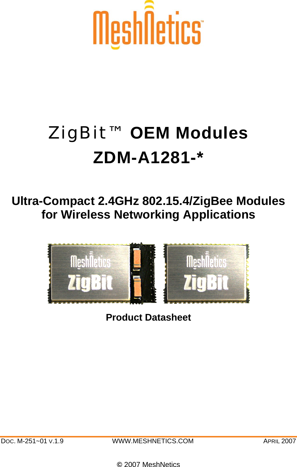
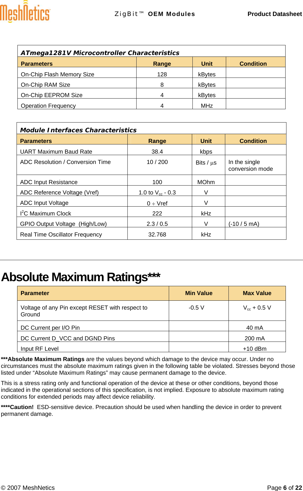
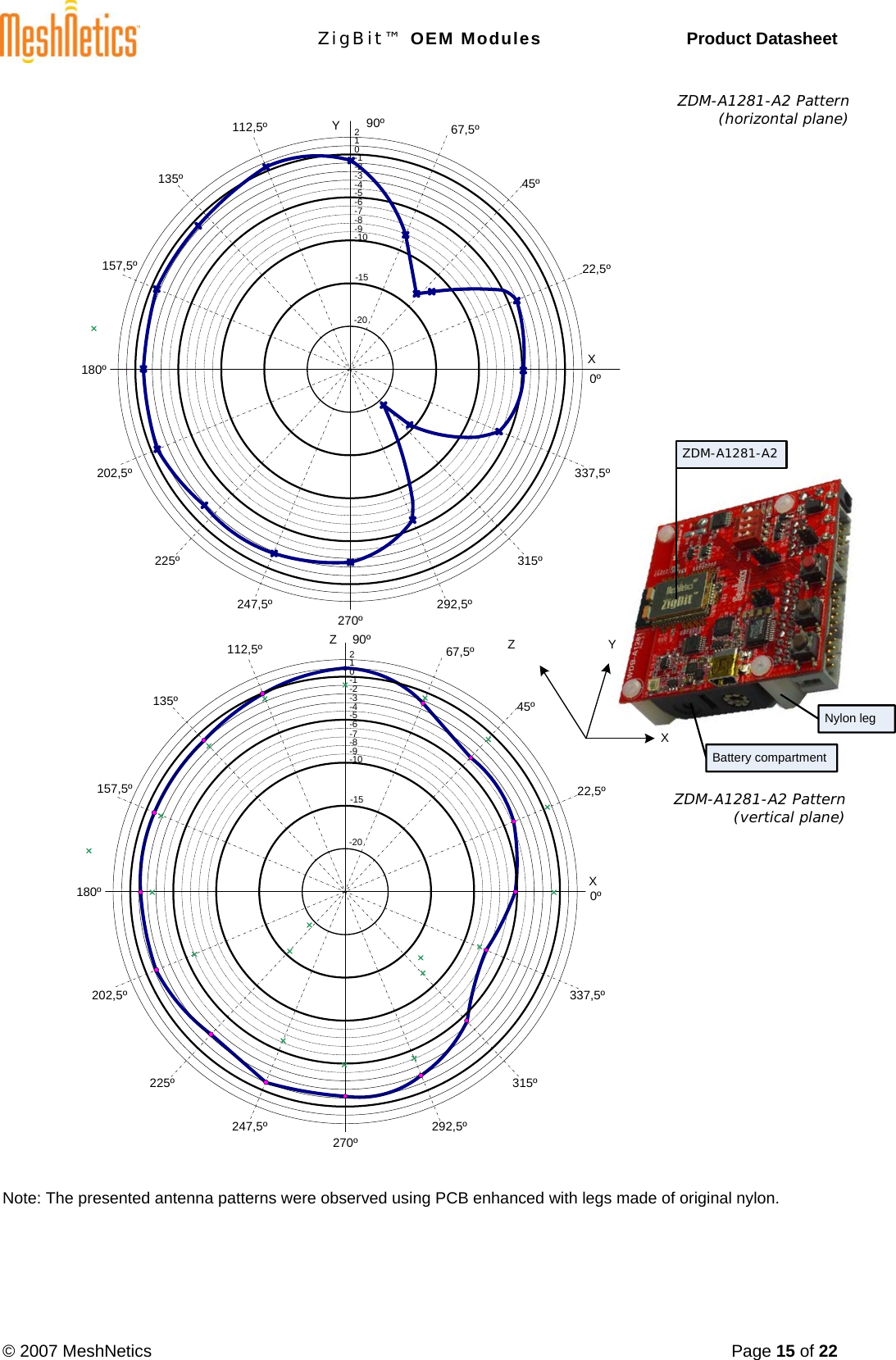
![ZigBit™ OEM Modules Product Datasheet © 2007 MeshNetics Page 4 of 22 AT86RF230RFTransceiverATmega1281Microcontroller RF I/OSPI BusGPIOVCC (1.8 – 3.6V)UARTI2CJTAGAnalogIRQUSART/SPIATmega1281MicrocontrollerSPI BusGPIOVCC (1.8 – 3.6V)UARTI2CJTAGAnalogIRQAT86RF230RFTransceiverChip AntennaUSART/SPI ZigBit™ Module Overview ZigBit is a low-power, high-sensitivity IEEE802.15.4/ ZigBee-2006 compliant OEM module. This multi-functional device occupies less than a square inch of space, which is comparable to a typical size of a single chip. Based on a solid combination of Atmel’s latest AVR Z-Link hardware platform [1], the ZigBit offers superior radio performance with exceptional ease of integration. ZigBit modules comply with the FCC (Part 15), IC and ETSI (CE) rules applicable to the devices radiating in uncontrolled environment. For details, see section Agency Certifications below. ZigBit fully satisfies the requirements of the “Directive 2002/95/EC of the European Parliament and the Council of 27January 2003 on the restriction of the use of certain hazardous substances in electrical and electronic equipment” (RoHS). MeshNetics provides fully compliant product in all regions where the directive is enforced July 1, 2006. The ZigBit contains Atmel’s ATmega1281V Microcontroller [1] and AT86RF230 RF Transceiver [2]. The module features 128kb flash memory and 8 kb RAM. The ZigBit already contains a complete RF/MCU-related design with all the necessary passive components included. The module can be easily mounted on a simple 2-layer PCB. Compared to a single-chip, a module-based solution offers considerable savings in development time & NRE cost per unit during the design & prototyping phase. Innovative (patent-pending) chip antenna design in ZDM-A1281-A2 module eliminates the balun and achieves good performance over ZigBee frequency band. MeshNetics provides tools for building ready-to-use applications around the ZigBit module. The Evaluation Kit and the Development Kit help prototyping and testing an 802.15.4 or ZigBee networking solution. It includes the sensor boards with multiple interfaces, an out-of-the-box data acquisition software suite, as well as accessories and documentation. The sample sensor data acquisition application allows network monitoring and data collection, all visualized via graphic interface. The ZigBit modules come bundled with the eZeeNet networking firmware. The eZeeNet enables the module-based OEM products to form self-healing, self-organizing mesh networks. The eZeeNet stack conforms to IEEE802.15.4/ ZigBee specifications [3], [4], [5]. Depending on your design requirements, you can use the ZigBit to operate a sensor node, where it would function as a single MCU. Or you can pair it to a host processor, where the module would serve essentially as a modem. In the former case, a user application should be bundled with the eZeeNet software. The eZeeNet’s programming interface gives users flexibility to manage network and minimize power consumption. ZDM-A1281-B0 Block Diagram ZDM-A1281-A2 Block Diagram eZeeNet™ Block Diagram](https://usermanual.wiki/LuxLabs-MeshNetics/ZIGBIT-A2/User-Guide-784667-Page-4.png)
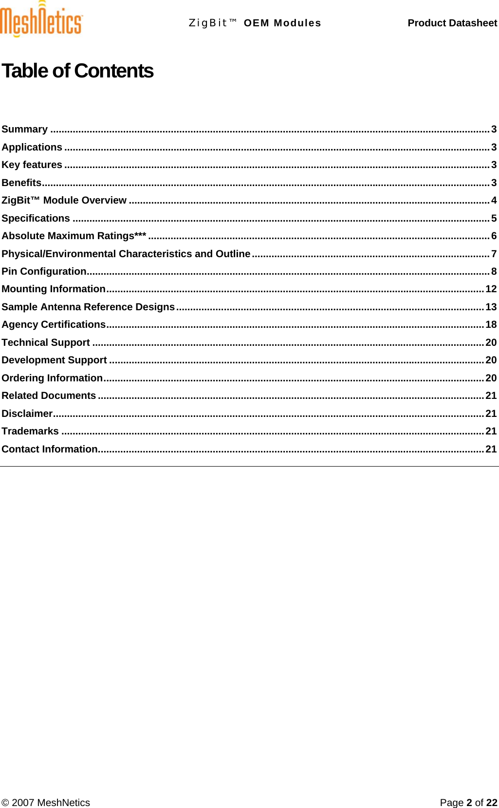
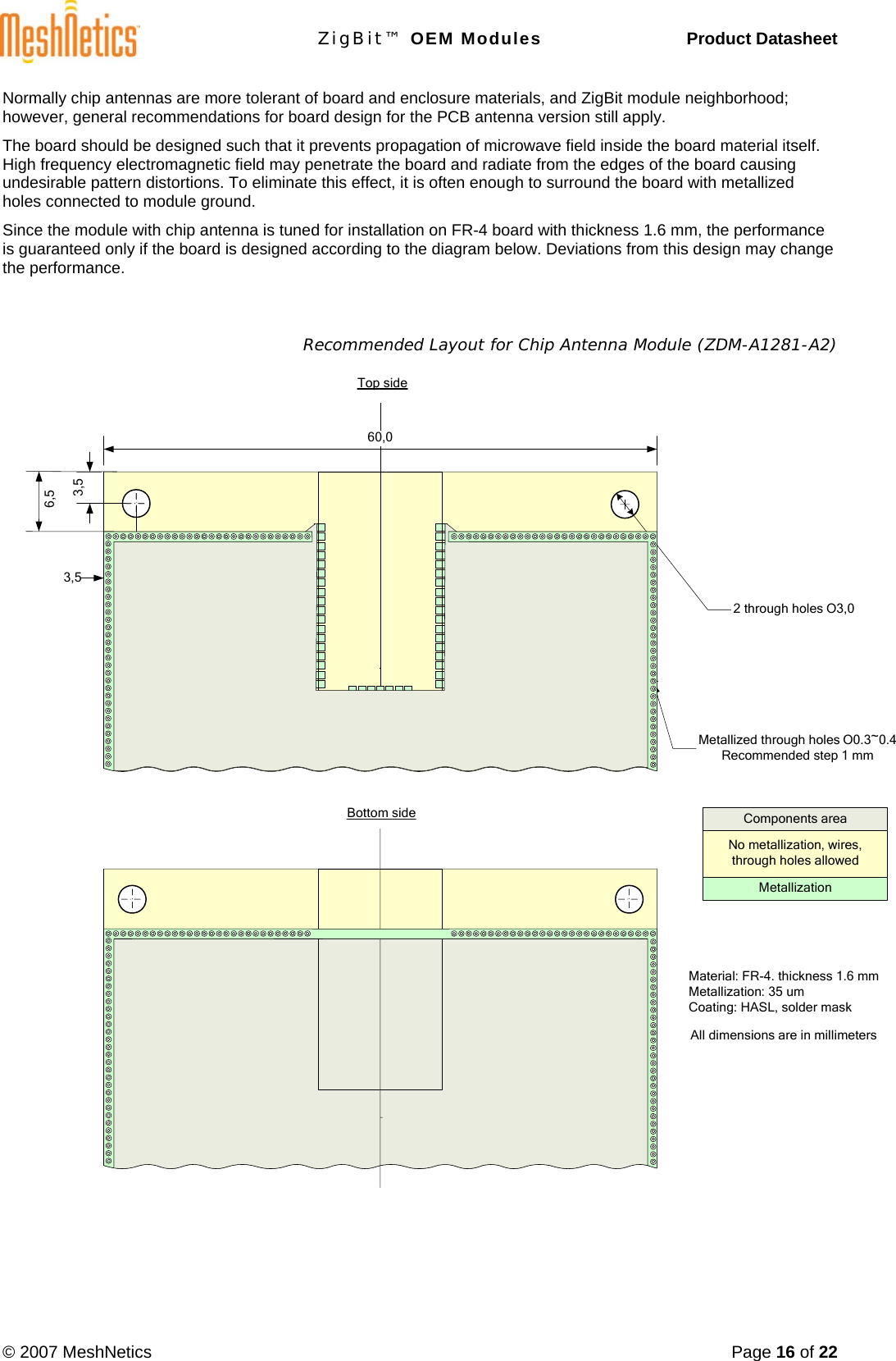
![ZigBit™ OEM Modules Product Datasheet © 2007 MeshNetics Page 10 of 22 Connector Pin Pin Name Description I/O Default State after power on Port ATmega 1281V ATmega 1281v Datasheet Reference* Notes, see list below 27 JTAG_TDI JTAG test data input I PF7 1, 2, 3, 5 28 JTAG_TDO JTAG test data output O PF6 1, 2, 3, 5 29 JTAG_TCK JTAG test clock I PF4 97, 288 1, 2, 3, 5 30 ADC_INPUT_3 ADC input channel 3 I tri-state PF3 1, 2, 6 31 ADC_INPUT_2 ADC input channel 2 I tri-state PF2 1, 2, 6 32 ADC_INPUT_1 ADC input channel 1 I tri-state PF1 1, 2, 6 33 BAT ADC input channel 0. Used by the stack for battery level measurement. Nominal voltage is 1 V in respect to AGND. I tri-state PF0 Pages 97, 266-287 1, 2, 6 34 A_VREF Output/Input reference voltage for ADC I/O tri-state AREF Pages 274, 280 35 AGND Analog ground 36 GPIO9 General purpose digital input/output 9 I/O PG5 1, 2, 3, 6 37 UART_DTR DTR input (Data Terminal Ready) for UART. Active low. I tri-state PE4 Pages 73, 93 1, 2, 3, 6 38 USART0_RXD UART/SPI receive pin I tri-state PE0 1, 2, 3, 6 39 USART0_TXD UART/SPI transmit pin O tri-state PE1 1, 2, 3, 6 40 USART0_EXTCLK UART/SPI external clock I tri-state PE2 Pages 198, 224, 198-232 1, 2, 3, 6 41 GPIO8 General purpose digital input/output 8 I/O tri-state PE3 1, 2, 3, 6 42 IRQ_7 Digital input interrupt request 7 I tri-state PE7 1, 2, 3, 6 43 IRQ_6 Digital input interrupt request 6 I tri-state PE6 Pages 73, 93-96 1, 2, 3, 6 44, 46, 48 RF_GND RF analog ground 9 45 RFP_IO Differential RF input/output. I/O 9 47 RFN_IO Differential RF input/output. I/O 9 Notes: 1. *Most of pins can be configured for general purpose I/O or for some alternative functions as described in details in the ATmega1281V Datasheet [1]. 2. GPIO pins can be programmed either for output, or input with/without pull-up resistors. Output pin drivers are strong enough to drive LED displays directly (refer to figures on pages 387-388, [1]). 3. All digital pins are provided with protection diodes to D_VCC and DGND 4. It is strongly recommended to avoid assigning an alternative function for OSC32K_OUT pin because it is used by eZeeNet Framework. However, this signal can be used if another peripheral or host processor requires 32.768 kHz clock, otherwise this pin can be disconnected. 5. Normally, JTAG_TMS, JTAG_TDI, JTAG_TDO, JTAG_TCK pins are used for on-chip debugging and flash burning. They can be used for A/D conversion if JTAGEN fuse is disabled. 6. eZeeNet software can configure as general-purpose I/O lines the following pins: GPIO0, GPIO1, GPIO2, GPIO3, GPIO4, GPIO5, GPIO6, GPIO7, GPIO8, GPIO9, I2C_CLK, I2C_DATA, UART_TXD, UART_RXD, UART_RTS, UART_CTS, ADC_INPUT_3, ADC_INPUT_2, ADC_INPUT_1, BAT, UART_DTR, USART0_RXD, USART0_TXD, USART0_EXTCLK, IRQ_7, IRQ_6. Additionally, four JTAG lines could be](https://usermanual.wiki/LuxLabs-MeshNetics/ZIGBIT-A2/User-Guide-784667-Page-10.png)
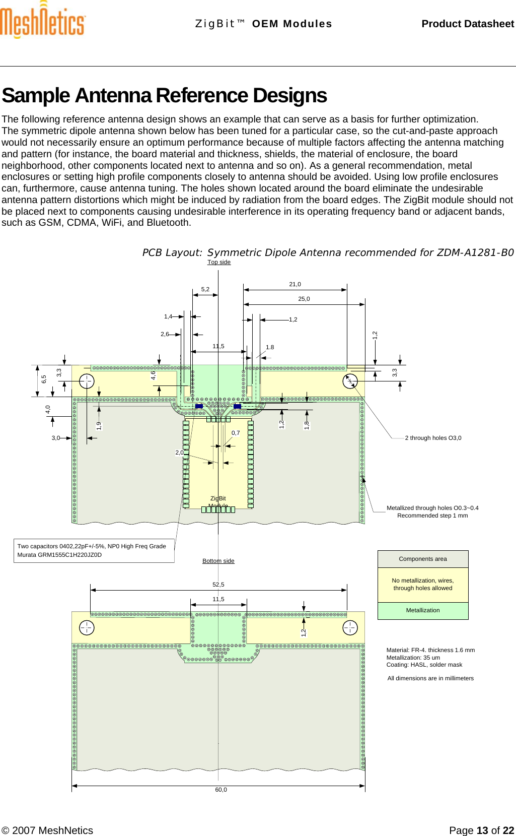
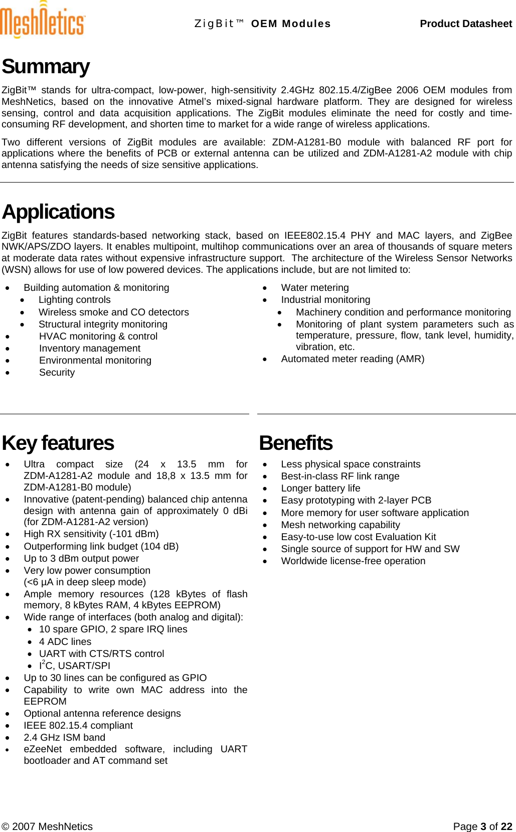
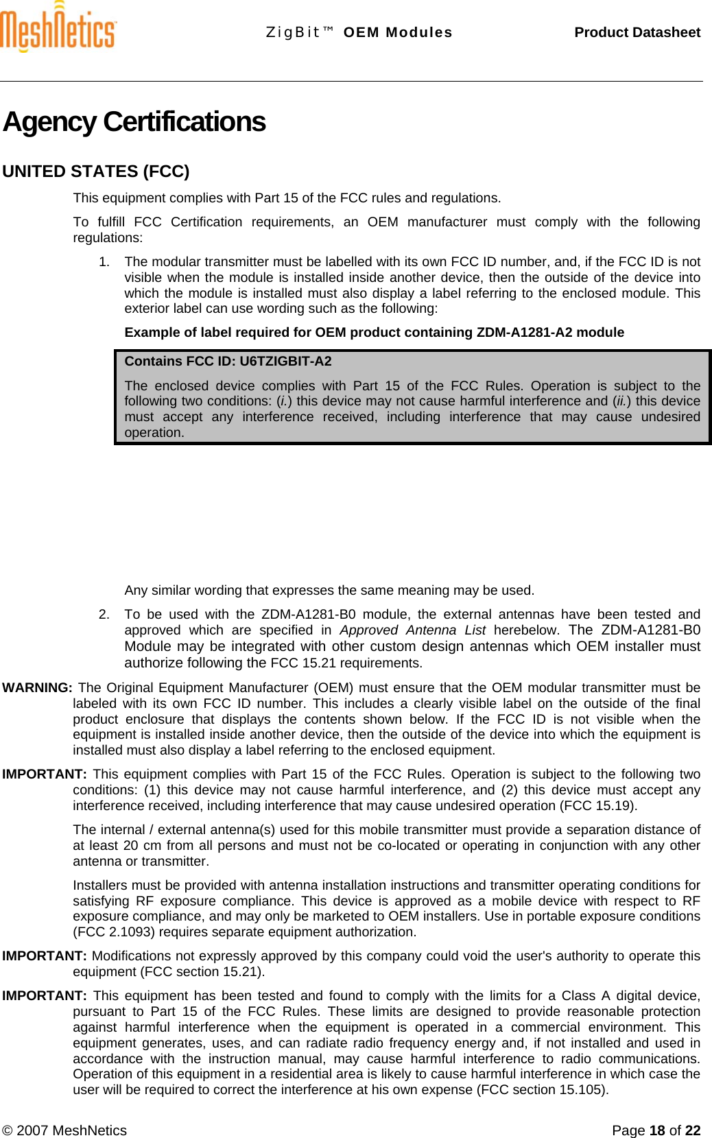
![ZigBit™ OEM Modules Product Datasheet © 2007 MeshNetics Page 17 of 22 Recommended PCB Layout for 50 Ohm External Antenna (ZDM-A1281-B0) Material: FR-4. thickness 1.6 mmMetallization: 35 umCoating: HASL, solder maskDetailed dimensions: see datasheets for Balun and SMA-ConnectorNo metallization, wires, through holes allowedMetallizationComponents areaTop sideBottom sideAll dimensions are in millimeters2,07,52,60,71,75,1Balun TDK’s HHM1520SMA-ConnectorMetallized through holes O0,3~0,4Recommended step 1 mm0,93,45,00,95,04 through holes O1,9Two capacitors 0402,22pF+/-5%, NP0 High Freq GradeMurata GRM1555C1H220JZ0D In case an external antenna or a 50 Ohm unbalanced antenna is required, they can be easily interfaced to ZigBit module ZDM-A1281-B0 by using 2:1 balun as shown above. This recommended sample demonstrates how to use low-profile Murata connector. It can be simply replaced with 50 Ohm microstrip line as shown in TDK’s HHM1520 Balun Datasheet [6].](https://usermanual.wiki/LuxLabs-MeshNetics/ZIGBIT-A2/User-Guide-784667-Page-17.png)

![ZigBit™ OEM Modules Product Datasheet © 2007 MeshNetics Page 21 of 22 Related Documents [1] Atmel 8-bit AVR Microcontroller with 64K/128K/256K Bytes In-System Programmable Flash. 2549F-AVR-04/06 [2] Atmel Low-Power Transceiver for ZigBee Applications. AT86RF230 Target Specification. 5131A-ZIGB-08/15/05 [3] IEEE Std 802.15.4-2003 IEEE Standard for Information technology – Part 15.4 Wireless Medium Access Control (MAC) and Physical Layer (PHY) Specifications for Low-Rate Wireless Personal Area Networks (LR-WPANs) [4] ZigBee Specification. ZigBee Document 053474r14, November 03, 2006 [5] eZeeNet™ IEEE802.15.4/ZigBee Software. Product Datasheet. MeshNetics Doc. M-251~02 [6] Multilayer Baluns, HHM Series. HHM1520 For Bluetooth & IEEE802.11b/g, www.tdk.co.jp/tefe02/e8balun_hhm.pdf Disclaimer MeshNetics believes that all information is correct and accurate at the time of issue. MeshNetics reserves the right to make changes to this product without prior notice. Please visit MeshNetics website for the latest available version. MeshNetics does not assume any responsibility for the use of the described product or convey any license under its patent rights. Trademarks MeshNetics®, ZigBit, eZeeNet, ZigBeeNet, SensiLink, LuxLabs, Luxoft Labs, and MeshNetics, Luxoft Labs and ZigBit logos are trademarks of LuxLabs Ltd. All other product names, trade names, trademarks, logos or service names are the property of their respective owners. © 2007 MeshNetics. All rights reserved. No part of the contents of this manual may be transmitted or reproduced in any form or by any means without the written permission of MeshNetics. Contact Information MeshNetics 9 Dmitrovskoye Shosse Moscow 127434, Russia Tel: +7 (495) 725 8125 Fax: +7 (495) 725 8116 E-mail: zigbit@meshnetics.com Website: www.meshnetics.com Office hours: 8:00am – 5:00pm (Central European Time)](https://usermanual.wiki/LuxLabs-MeshNetics/ZIGBIT-A2/User-Guide-784667-Page-21.png)