MMB Research ZGB357PA10 RAPIDSE ZIGBEE SMART ENEGRY User Manual
MMB Research Inc. RAPIDSE ZIGBEE SMART ENEGRY Users Manual
UserManual.wiki
>
MMB Research
>
ZGB357PA10 User Manual
Users Manual
Navigation menu
Upload a User Manual
Namespaces
Wiki Guide
HTML
PDF
Info
Views
User Manual
Discussion / Help
Navigation
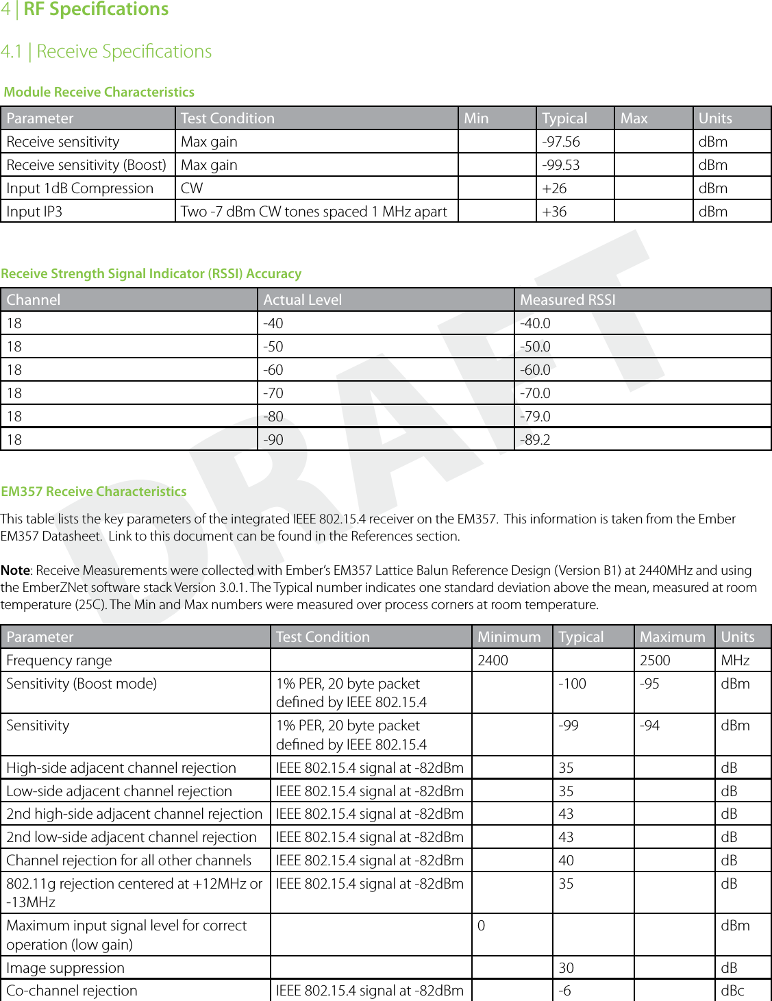
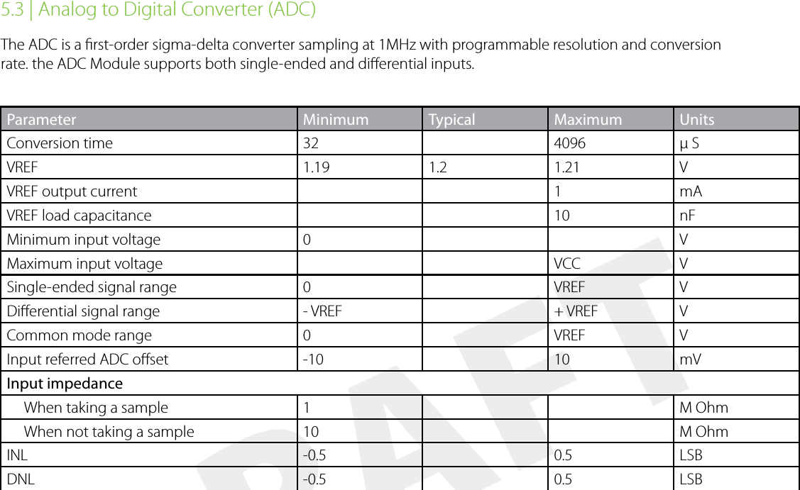
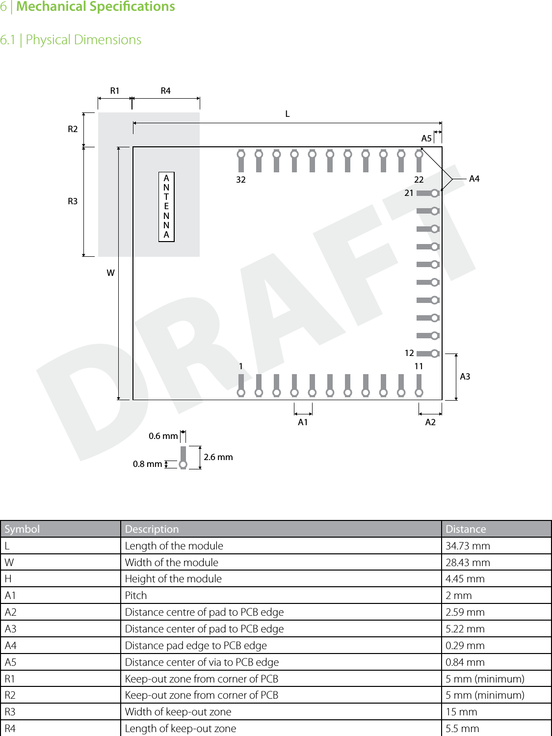
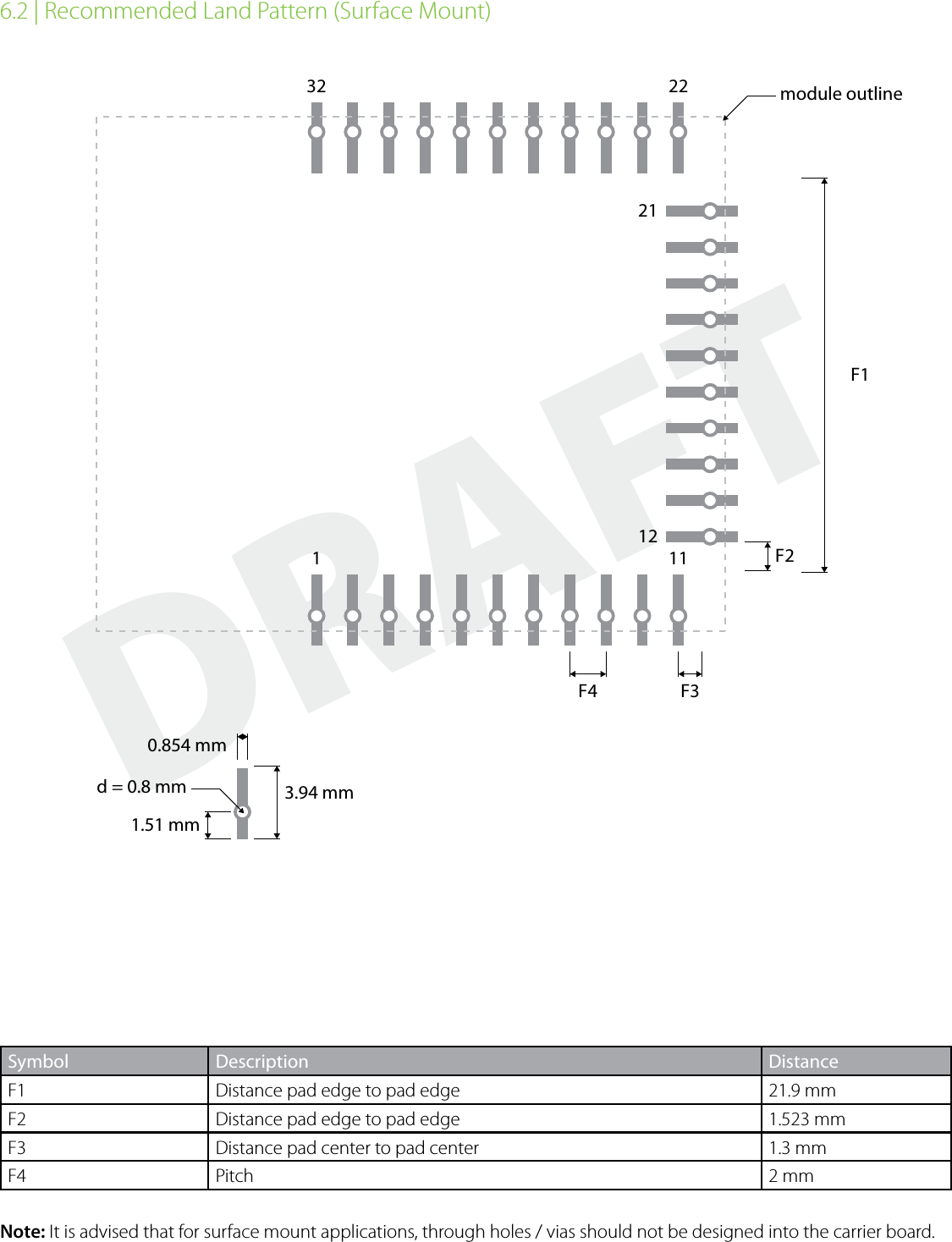
![DRAFT3 | Electrical Specications3.1 | Absolute Maximum Ratings3.2 | Recommended Operating Conditions3.3 | DC Electrical CharacteristicsParameter Minimum Maximum UnitsSupply Voltage (VCC) -0.3 3.6 VVoltage on any GPIO[0:16], SIF CLK, SIF MISO, SIF MOSI, nSIF LOAD, nReset -0.3 VCC +0.3 VAmbient Operating Temperature -40 +85 °CStorage Temperature -40 +125 °CParameter Minimum Typical Maximum UnitsSupply Voltage (VCC) 2.7 3.3 3.6 VTemperature Range -40 +85 °CParameter Test Condition Minimum Typical Maximum UnitsDeep sleep current At 25 °C, VCC = 3.3v, shutdown mode10.5 µAIdle current At 25 °C, VCC = 3.3v, sleep mode7.8 mARX current At 25 °C, VCC = 3.3v 36 mATX current At 25 °C, VCC = 3.3v, boost mode220 mATX current At 25 °C, VCC = 3.3v, normal mode190 mAInput voltage for logic 0 0 0.2 x VCC VInput voltage for logic 1 0.8 x VCC VCC VInput current for logic 0 -0.5 µAInput current for logic 1 0.5 µAInput pull-up resistor value 30 kΩInput pull-down resistor value 30 kΩOutput voltage for logic 0 0 0.18 x VCC VOutput voltage for logic 1 0.82 x VCC VCC VOutput source current(standard current pad)4 mAOutput sink current (standard current pad)4 mAOutput source current (high current pad: GPIO[16:13] )8 mAOutput sink current(high current pad: GPIO[16:13] )8 mATotal output current(for I/O pads)40 mA](https://usermanual.wiki/MMB-Research/ZGB357PA10/User-Guide-1348875-Page-3.png)
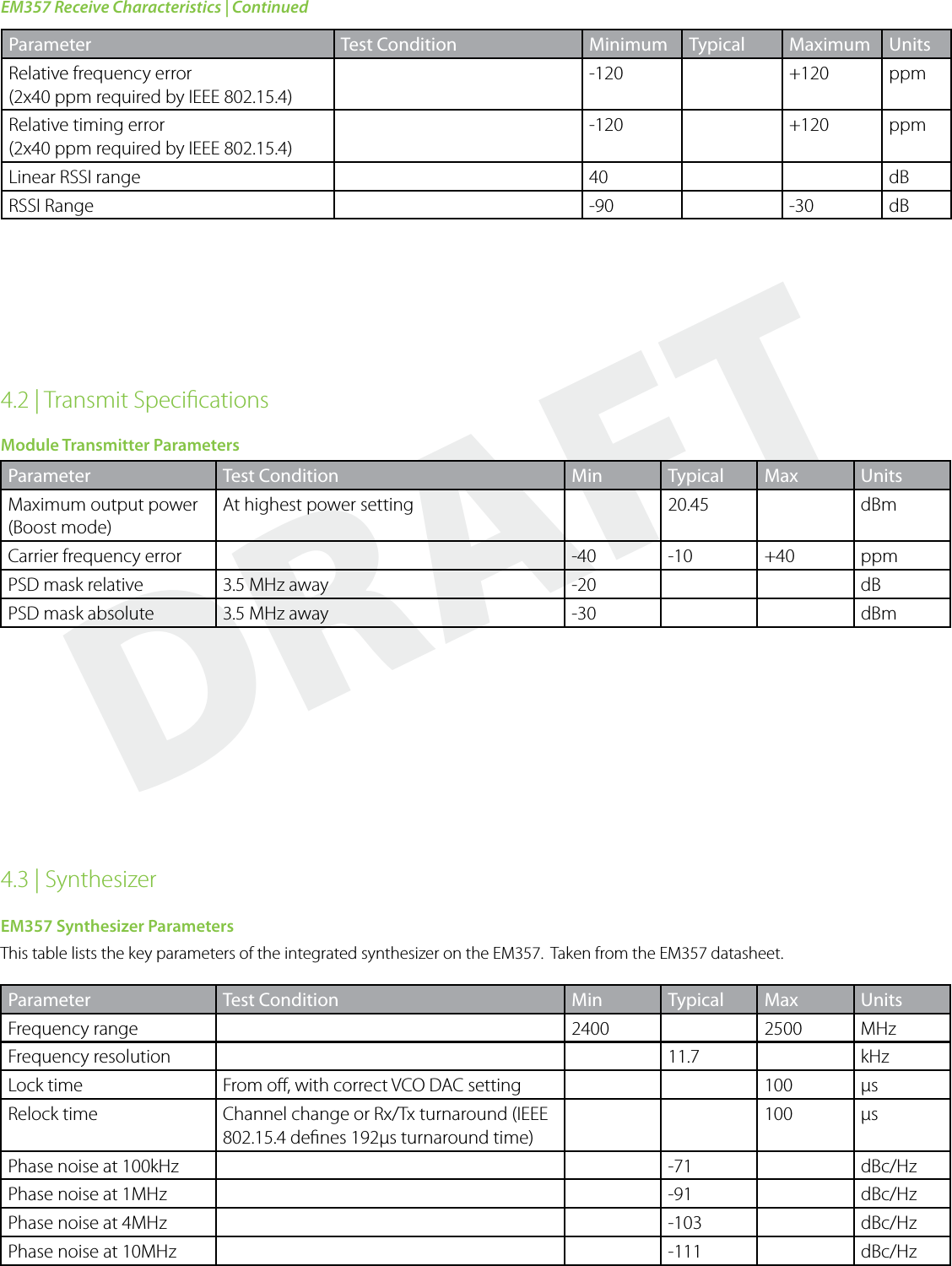
![DRAFT7 | Soldering Temperature Time Prole for reow soldering (Lead-free solder)150˚C - 190˚C220˚C30 +20/-10s90 ±30s230˚C - 240˚C maxTemp[ ˚C ]Time [ s ]Maximum reflow cycles: 2Opposite-side reflow is prohibited due to the module weight. You must not place the module on the bottom / underside of your PCB and re-flow.6.3 | Connector Specifications6.4 | Labelling6.3.1 | Edge Mount (USNAP) Connector6.3.2 | SIP Header / Socket10 pin 2mm pitch right angle female header11 + 11 + 10 (if no USNAP populated) pin 2mm pitch 0.8mm diameter through hole footprint20 mm20 mm](https://usermanual.wiki/MMB-Research/ZGB357PA10/User-Guide-1348875-Page-11.png)