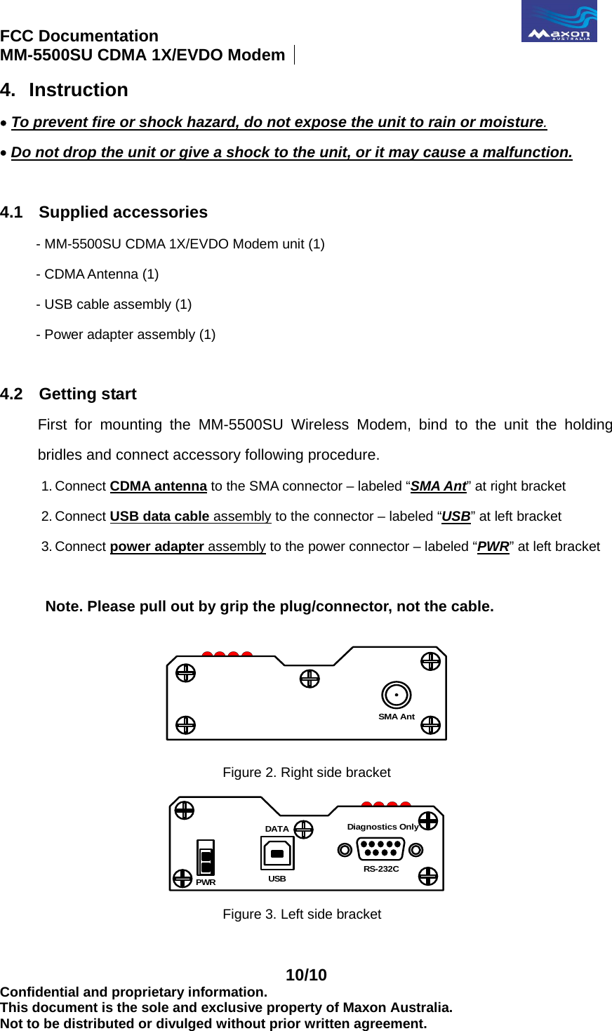
Maxon Electronics Australia MM-5500SU 800 MHz EVDO CDMA Wireless USB Modem User Manual FCC MM5500SU
Maxon Electronics Australia Pty. Ltd. 800 MHz EVDO CDMA Wireless USB Modem FCC MM5500SU
UserManual.wiki
>
Maxon Electronics Australia
>
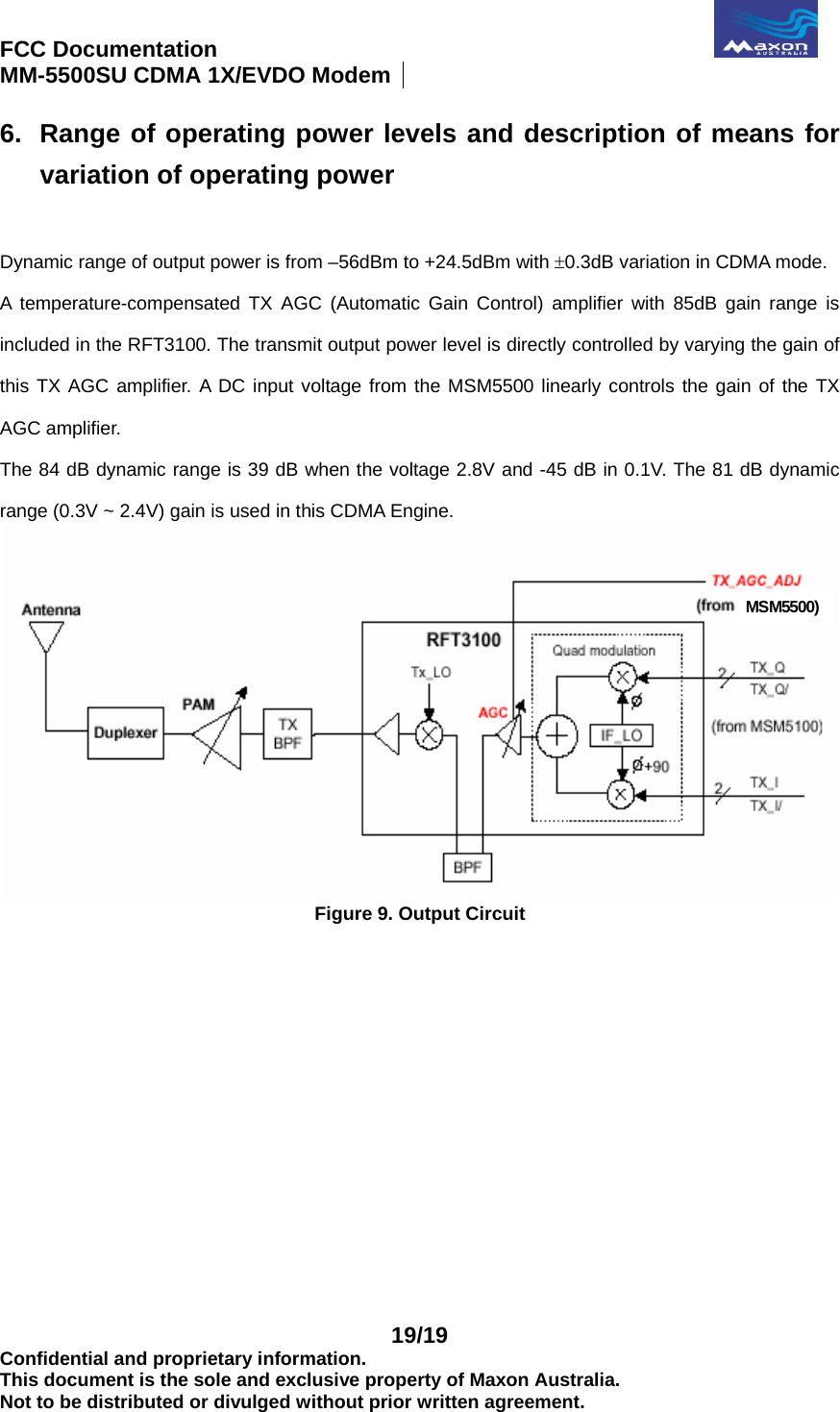
MM 5500SU User Manual
Users Manual
Navigation menu
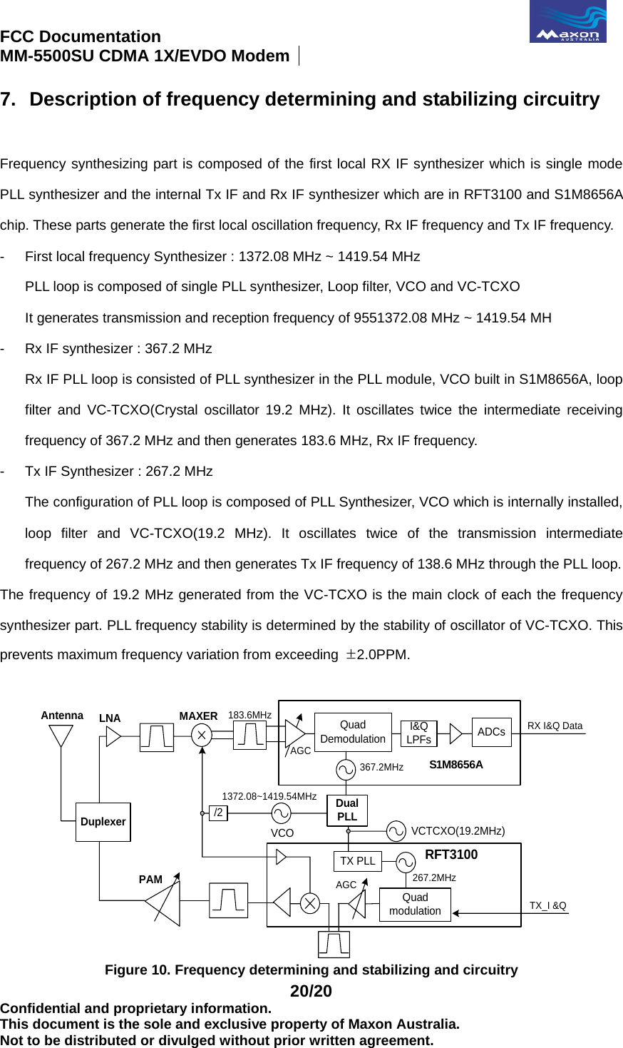
Upload a User Manual
Namespaces
Wiki Guide
HTML
PDF
Info
Views
User Manual
Discussion / Help
Navigation
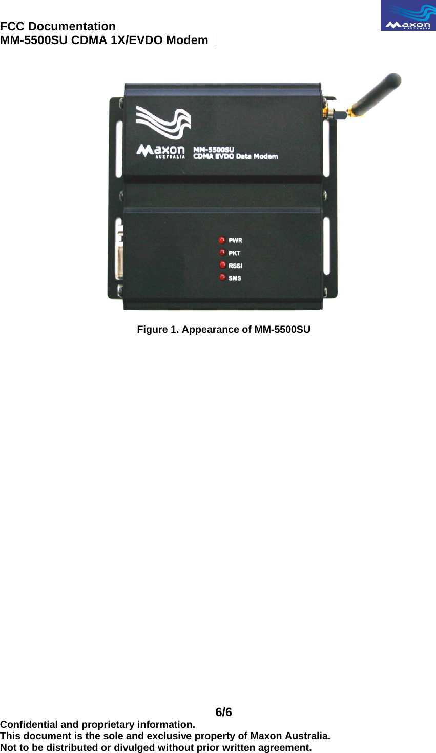
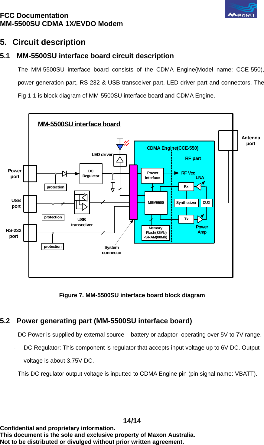
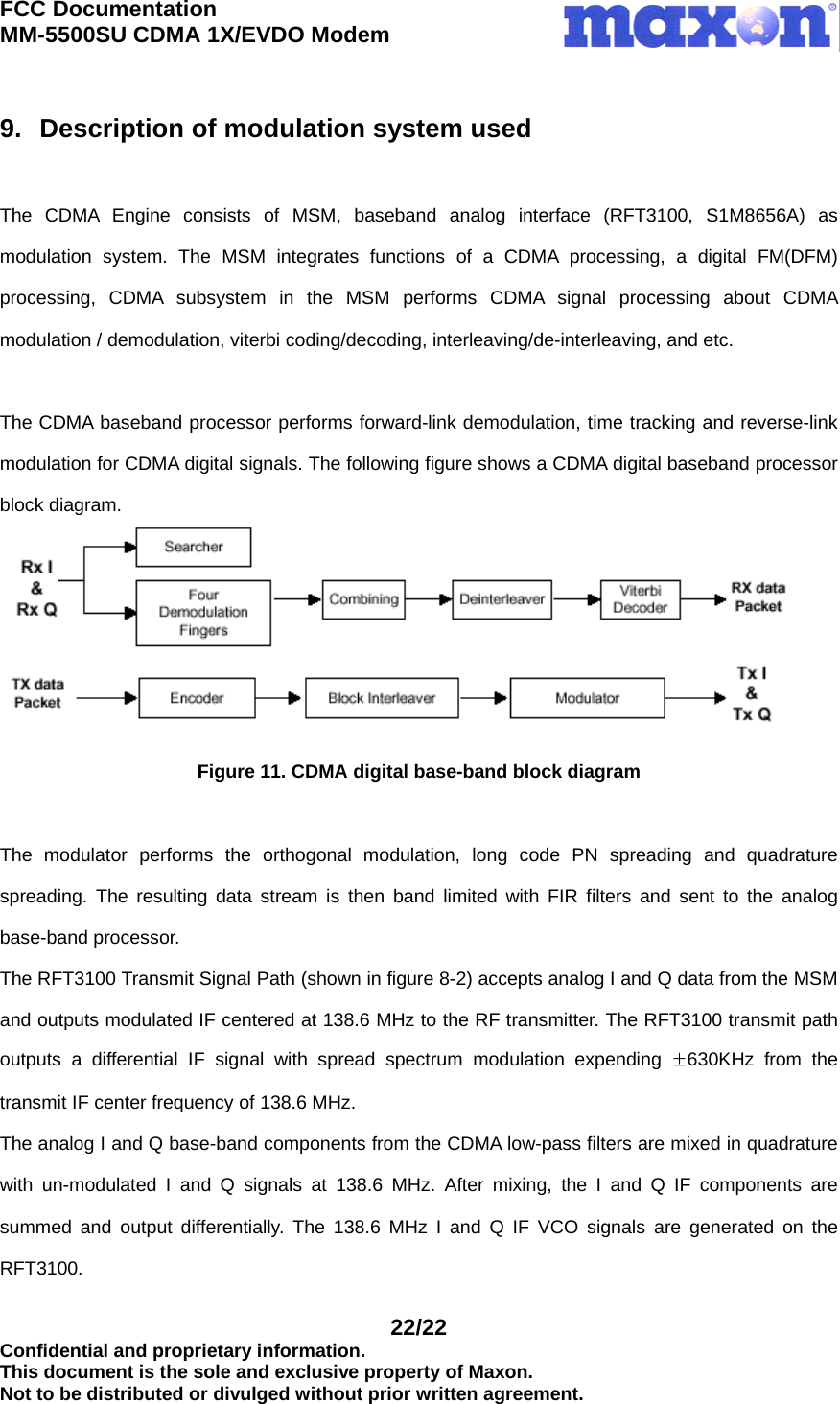
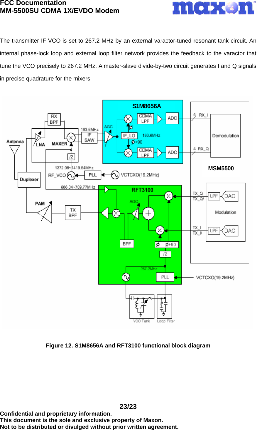
![FCC Documentation MM-5500SU CDMA 1X/EVDO Modem 5/5 Confidential and proprietary information. This document is the sole and exclusive property of Maxon Australia. Not to be distributed or divulged without prior written agreement. 2. Product Overview 2.1 Overview The MM-5500SU Wireless Modem performs data communication functions between Host and IS-95A, B, CDMA2000-1X/EVDO CDMA Cellular station. The MM-5500SU Wireless Modem incorporates the wireless-modem functionality with the USB driver and power adaptor interface. The MM-5500SU Wireless Modem connects directly to HOST computer utilizing an USB V1.1 interface. The MM-5500SU Wireless Modem functionality is specifically controlled from the Host via AT command sets. Range of supply voltage is from 5V to 7V on communication and 5V to 9V on idle. The power saving mode of the MM-5500SU Wireless Modem is controlled from the Host via USB port using AT command. 2.2 What is the MM-5500SU Wireless Modem - IS-95A, B, and CDMA2000-1XEVDO CDMA Protocol Support - USB1.1 Interface for data communication & Standard RS-232C for DM(Diagnostic Mode) - Remote controlled by AT commands - Comprehensive internal monitoring alerts - 5 user profiles - DATA Transmission up to 2.4[Mbps] (network limited) - LED indicating of the modem status - SMS 2-way support - SMA antenna connector - Secure 2-pin power jack - Operating voltage of DC 5~9[V] - Contemporary design - Small size and light-weight](https://usermanual.wiki/Maxon-Electronics-Australia/MM-5500SU/User-Guide-506360-Page-5.png)