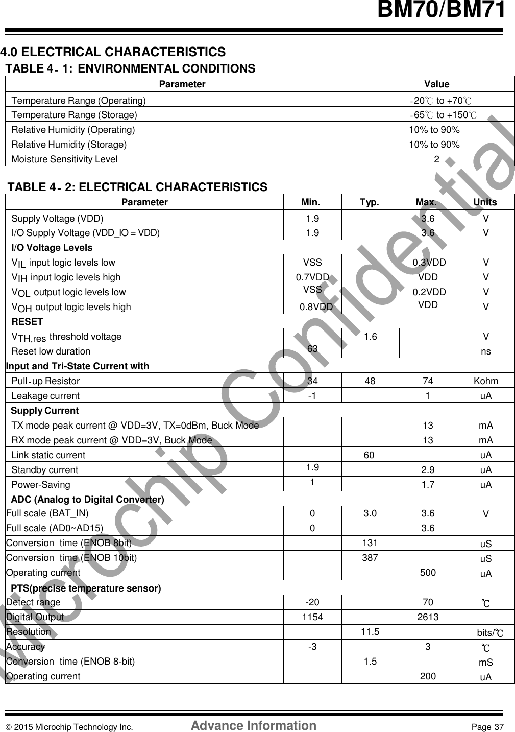
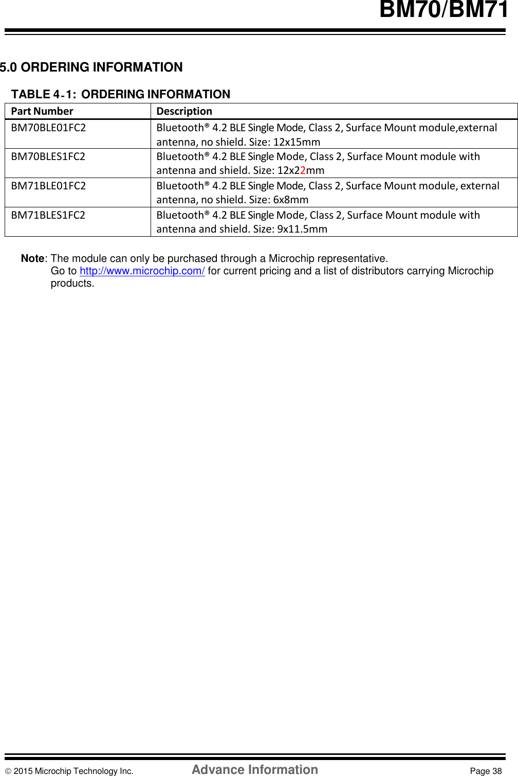
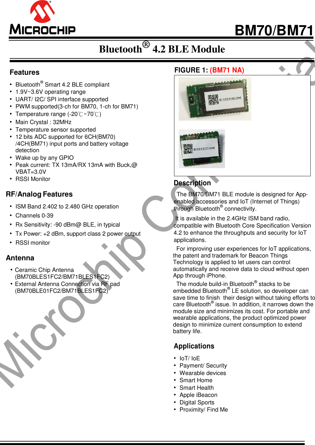
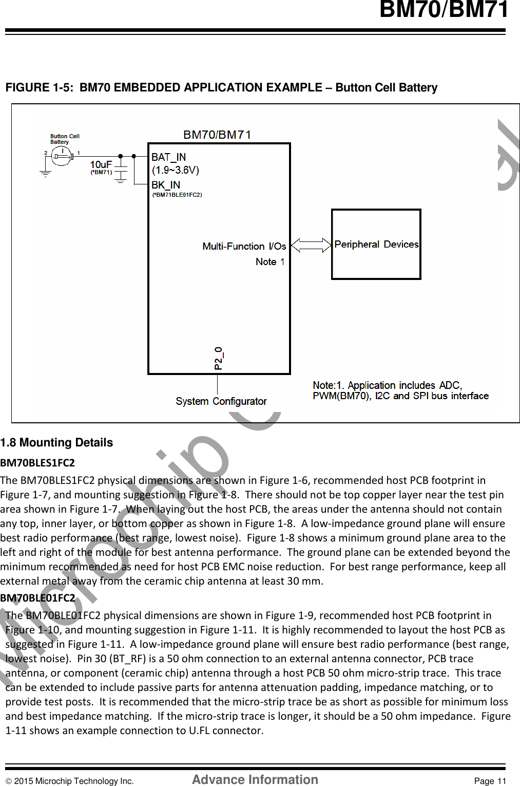
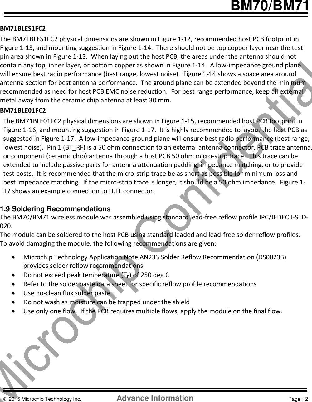
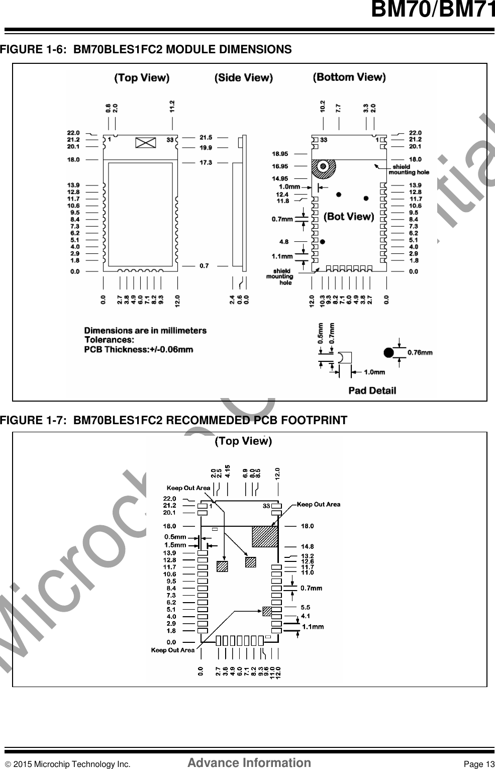
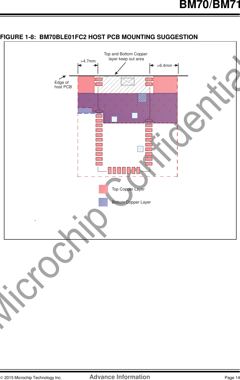
Microchip Technology BM70ABCDEFGH Bluetooth Module User Manual RN4020 Bluetooth Low Energy Module Data Sheet
Microchip Technology Inc. Bluetooth Module RN4020 Bluetooth Low Energy Module Data Sheet
UserManual.wiki
>
Microchip Technology
>
BM70ABCDEFGH User Manual
Manual
Navigation menu
Upload a User Manual
Namespaces
Wiki Guide
HTML
PDF
Info
Views
User Manual
Discussion / Help
Navigation

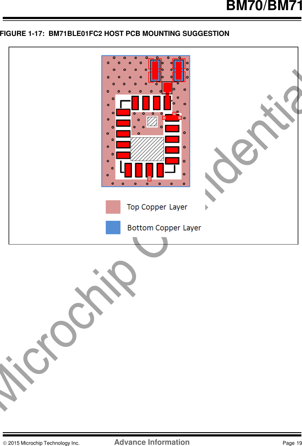
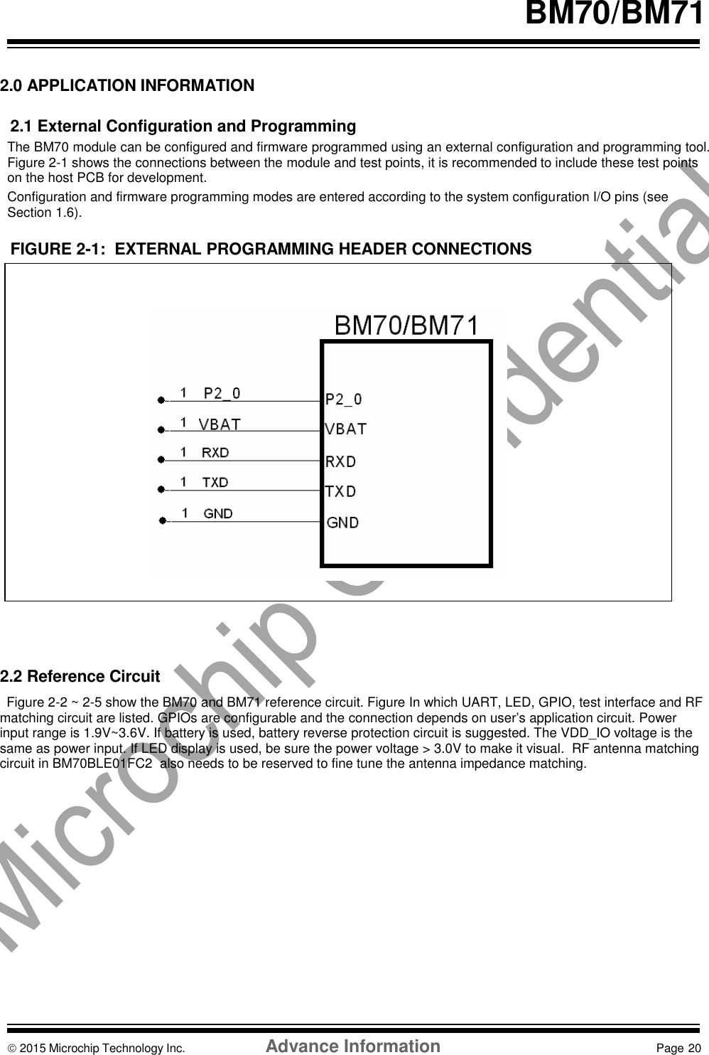
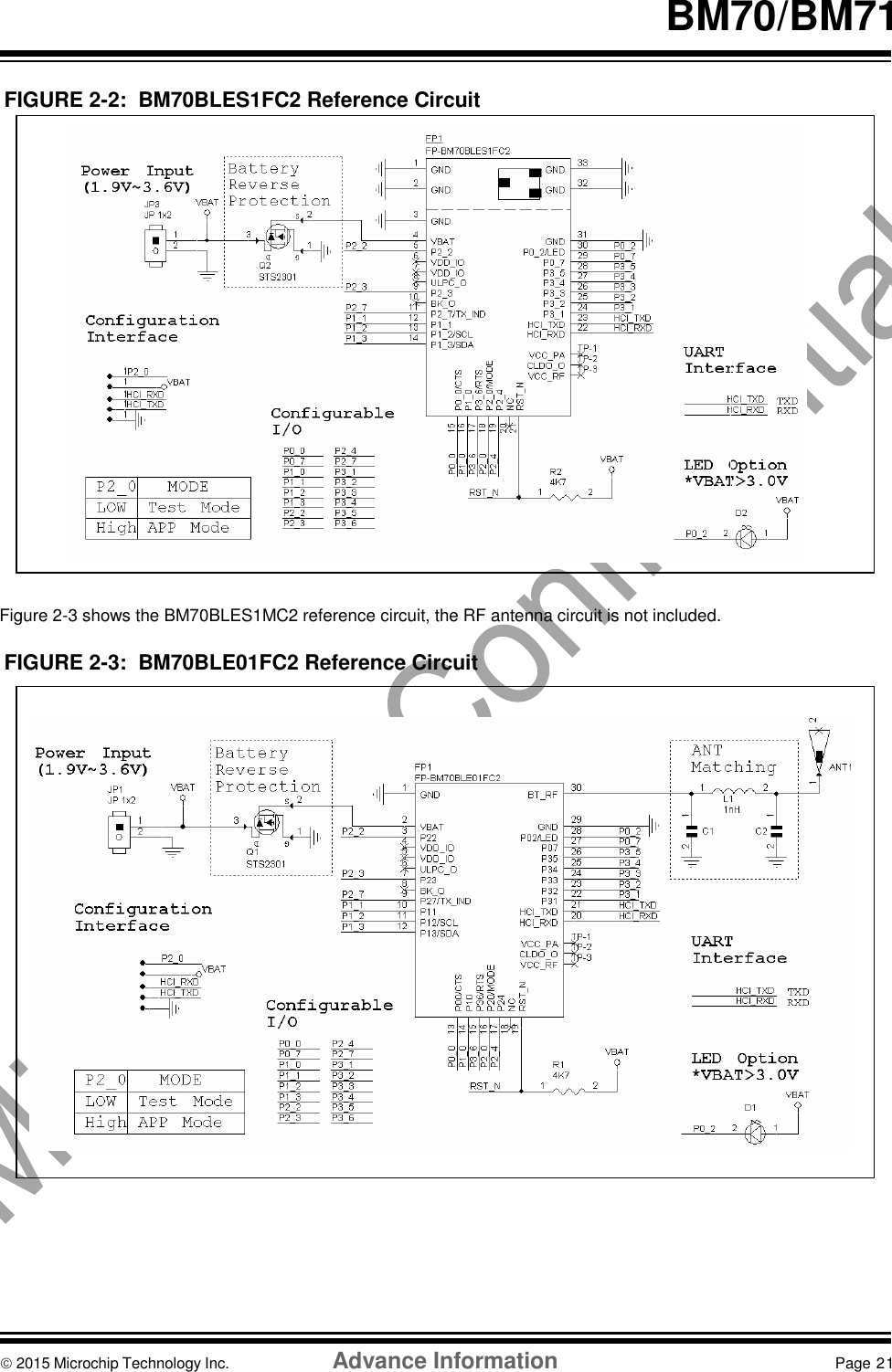
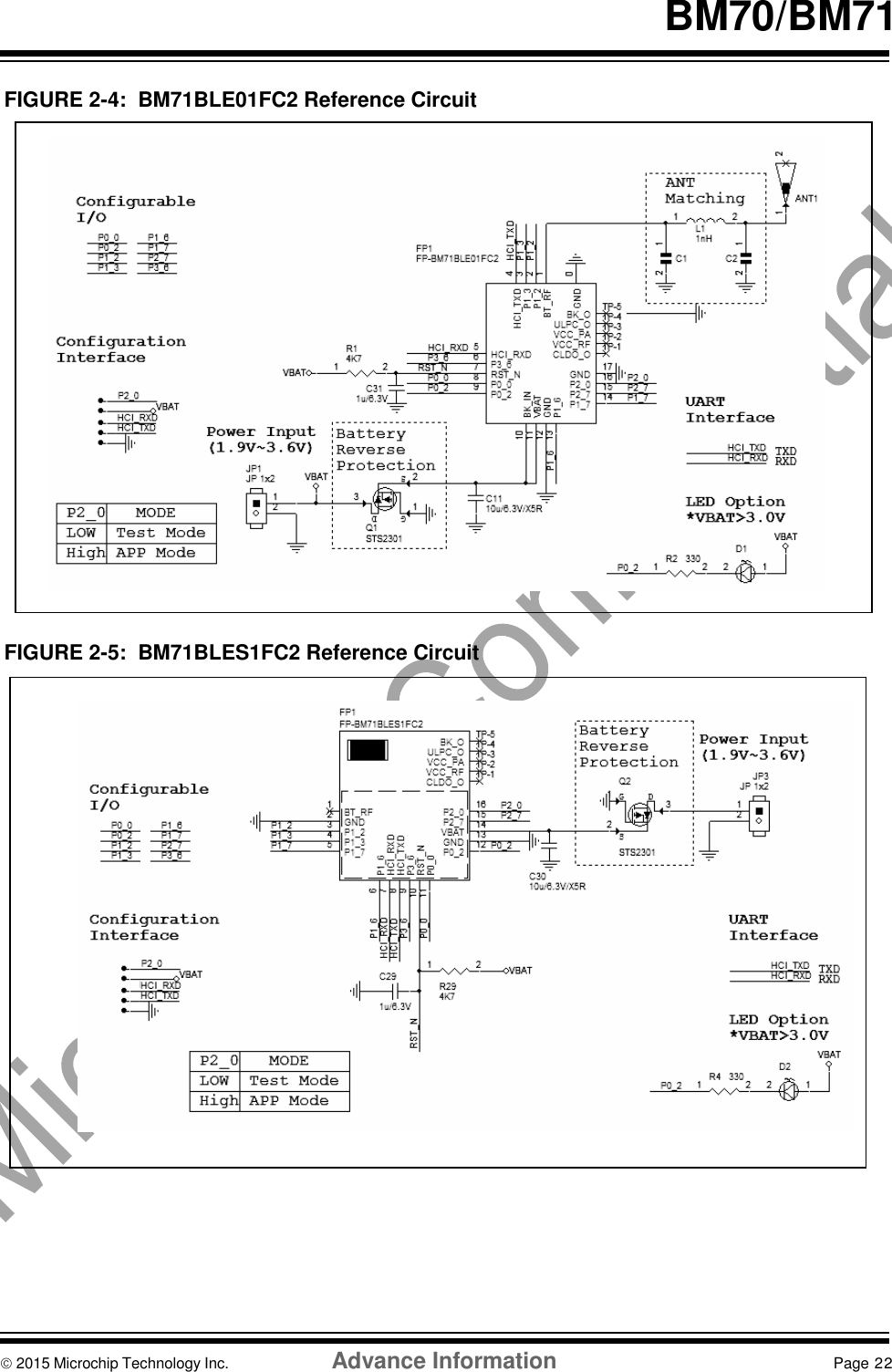
![BM70/BM71 3.3 Europe The BM70BLES1FC2 module is an R&TTE Directive assessed radio module that is CE marked and has been manufactured and tested with the intention of being integrated into a final product. The BM70 module has been tested to R&TTE Directive 1999/5/EC Essential Requirements for Health and Safety (Article (3.1(a)), Electromagnetic Compatibility (EMC) (Article 3.1(b)), and Radio (Article 3.2) and are summarized in Table 3‐1: European Compliance Testing. A Notified Body Opinion has also been issued. All test reports are available on the BM70 product web page at http://www.microchip.com/bm70. The R&TTE Compliance Association provides guidance on modular devices in document Technical Guidance Note 01 available at http://www.rtteca.com/html/download_area.htm. Note: To maintain conformance to the testing listed in Table 3‐1: European Compliance Testing, the module shall be installed in accordance with the installation instructions in this data sheet and shall not be modified. When integrating a radio module into a completed product the integrator becomes the manufacturer of the final product and is therefore responsible for demonstrating compliance of the final product with the essential requirements of the R&TTE Directive. 3.1.3 LABELING AND USER INFORMATION REQUIREMENTS The label on the final product which contains the BM70 module must follow CE marking requirements. The R&TTE Compliance Association Technical Guidance Note 01 provides guidance on final product CE marking. 3.1.4 ANTENNA REQUIREMENTS From R&TTE Compliance Association document Technical Guidance Note 01: Provided the integrator installing an assessed radio module with an integral or specific antenna and installed in conformance with the radio module manufacturer’s installation instructions requires no further evaluation under Article 3.2 of the R&TTE Directive and does not require further involvement of an R&TTE Directive Notified Body for the final product. [Section 2.2.4] The European Compliance Testing listed in Table 3‐1 was performed using the integral ceramic chip antenna. TABLE 3‐1: EUROPEAN COMPLIANCE TESTING Certification Standards Article Laboratory Report Number Date Safety EN 60950‐1:2006+A11:2009+A1:2010 (3.1(a)) Health EN 50371:2002‐03 EMC EN 301 489‐1 V1.8.1 (2008‐04) (3.1(b)) EN 301 489‐17 V2.1.1 (2009‐05) Radio EN 300 328 V1.7.1 (2006‐10) (3.2) Notified Body Opinion 2015 Microchip Technology Inc. Advance Information Page 32 BM70/BM71 3.3.3 HELPFUL WEB SITES](https://usermanual.wiki/Microchip-Technology/BM70ABCDEFGH/User-Guide-2759438-Page-33.png)