MtM Plus Technology M905 M905 User Manual M905 Product Specification v1 0 20161214
MtM Plus Technology Corporation M905 M905 Product Specification v1 0 20161214
UserManual.wiki
>
MtM Plus Technology
>
M905 User Manual
Users Manual
Navigation menu
Upload a User Manual
Namespaces
Wiki Guide
HTML
PDF
Info
Views
User Manual
Discussion / Help
Navigation
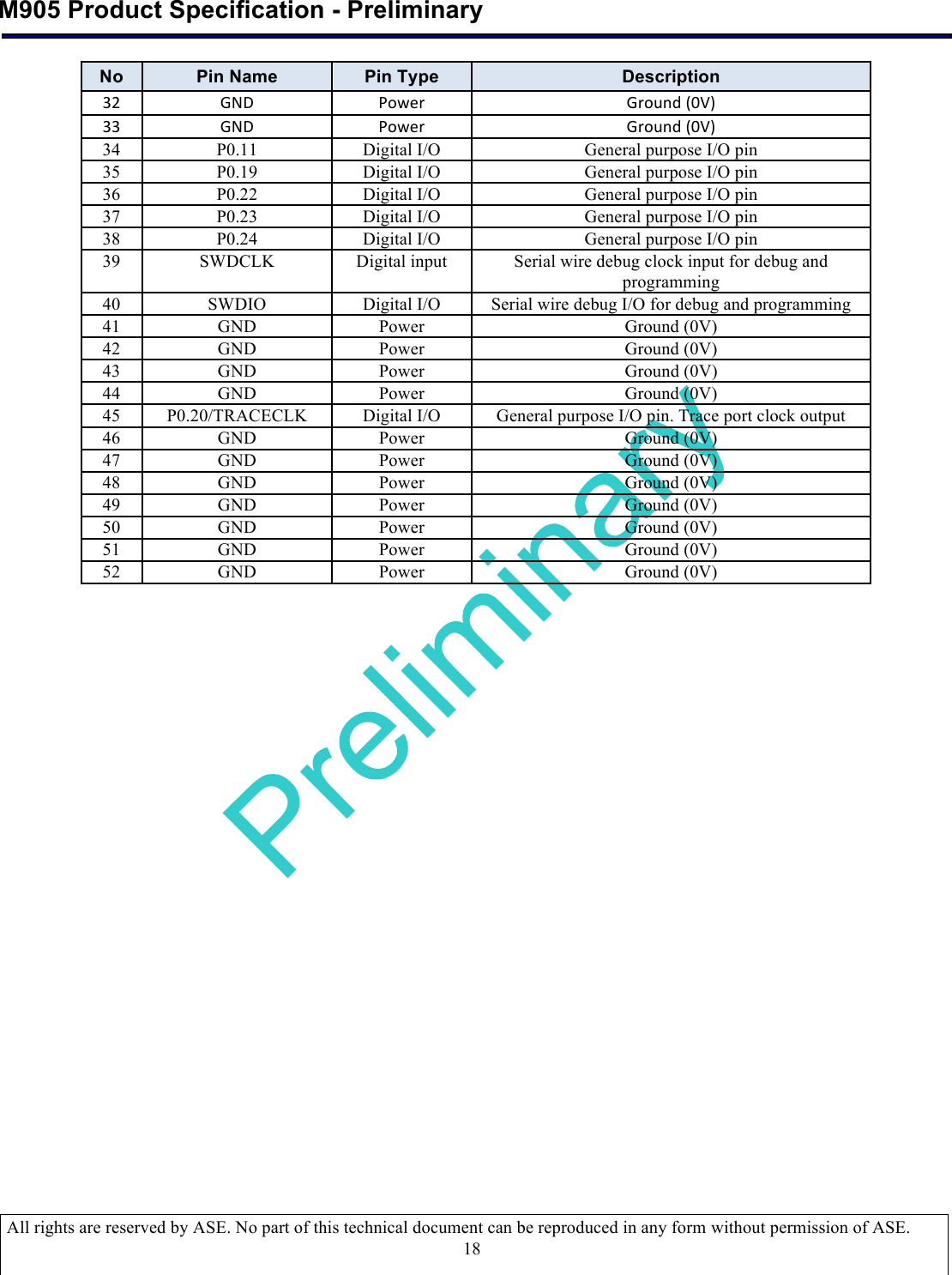
![M905 Product Specification - Preliminary All rights are reserved by ASE. No part of this technical document can be reproduced in any form without permission of ASE. 17 6. PIN DEFINITION The foot print dimension and pin definition is defined as below No Pin Name Pin Type Description 1!Antenna!Leg!RF!Scenario!B!2!GNDA1!RF!Scenario!A!3!GNDA2!RF!Scenario!A!4!GND!Power!Ground!(0V)!5!ANT!RF!Single-endded!radio!antenna!connection!6!RF!RF!Single-endded!radio!antenna!connection!7!GND!Power!Ground!(0V)!8!GND!Power!Ground!(0V)!9!VDD!Power!Power!supply!10!GND!Power!Ground!(0V)!11!GND!Power!Ground!(0V)!12!P0.21/nRESET!Digital!I/O!General!purpose!I/O!pin.!Configurable!as!system!RESET!pin!13!P0.14/TRACEDATA[3]!Digital!I/O!General!purpose!I/O!pin.!Trace!port!output!14!P0.15/TRACEDATA[2]!Digital!I/O!General!purpose!I/O!pin.!Trace!port!output!15!P0.16/TRACEDATA[1]!Digital!I/O!General!purpose!I/O!pin.!Trace!port!output!16!P0.18/TRACEDATA[0]!Digital!I/O!General!purpose!I/O!pin.!Trace!port!output!17!P0.00/XL1!Digital!I/O!Analog!input!General!purpose!I/O!pin.!Connection!for!32.768kHz!crystal!(LFXO)!18!P0.01/XL2!Digital!I/O!Analog!input!General!purpose!I/O!pin.!Connection!for!32.768kHz!crystal!(LFXO)!19!P0.03/AIN1!Digital!I/O!Analog!input!General!purpose!I/O!pin.!SAADC/COMP/LPCOMP!input!20!P0.02/AIN0!Digital!I/O!Analog!input!General!purpose!I/O!pin.!SAADC/COMP/LPCOMP!input!21!P0.09/NFC1!Digital!I/O!NFC!input!General!purpose!I/O!pin.!NFC!antenna!connection!22!P0.10/NFC2!Digital!I/O!NFC!input!General!purpose!I/O!pin.!NFC!antenna!connection!23!P0.05/AIN3!Digital!I/O!Analog!input!General!purpose!I/O!pin.!SAADC/COMP/LPCOMP!input!24!P0.04/AIN2!Digital!I/O!Analog!input!General!purpose!I/O!pin.!SAADC/COMP/LPCOMP!input!25!P0.31/AIN7!Digital!I/O!Analog!input!General!purpose!I/O!pin.!SAADC/COMP/LPCOMP!input!26!P0.30/AIN6!Digital!I/O!Analog!input!General!purpose!I/O!pin.!SAADC/COMP/LPCOMP!input!27!P0.29/AIN5!Digital!I/O!Analog!input!General!purpose!I/O!pin.!SAADC/COMP/LPCOMP!input!28!P0.28/AIN4!Digital!I/O!Analog!input!General!purpose!I/O!pin.!SAADC/COMP/LPCOMP!input!29!P0.27!Digital!I/O!General!purpose!I/O!pin!30!P0.25!Digital!I/O!General!purpose!I/O!pin!31!P0.26!Digital!I/O!General!purpose!I/O!pin!](https://usermanual.wiki/MtM-Plus-Technology/M905/User-Guide-3642735-Page-16.png)