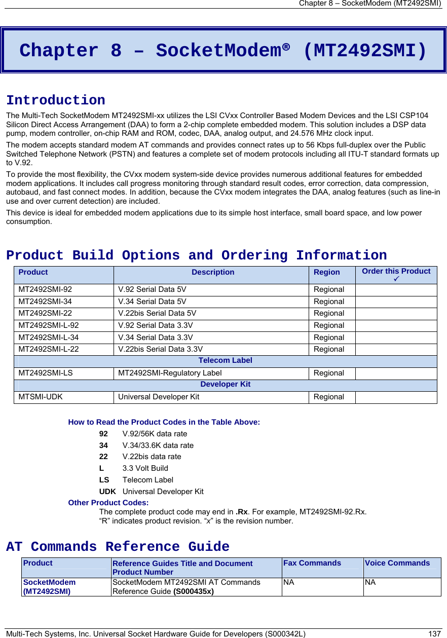
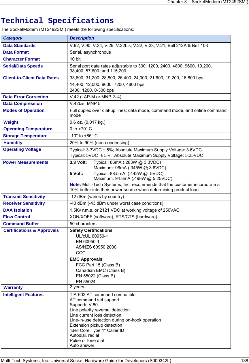
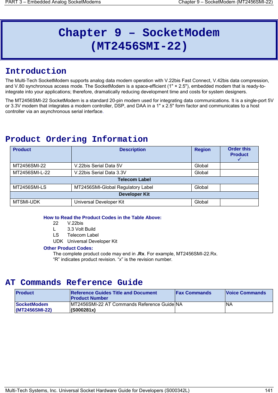
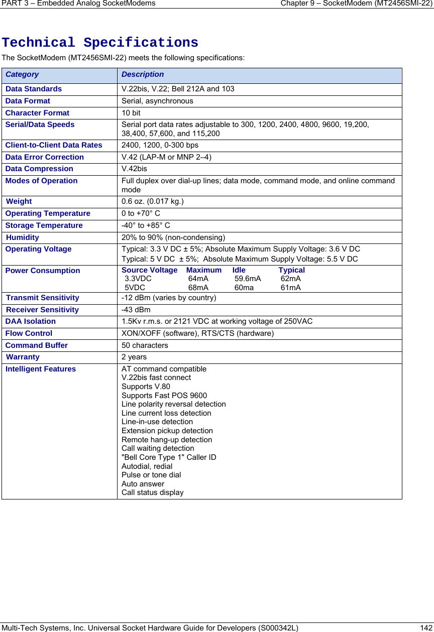
Multi Tech Systems 92U09G17825 SocketModem CDMA User Manual MTSMC C1 DRAFT S000342L
Multi Tech Systems Inc SocketModem CDMA MTSMC C1 DRAFT S000342L
UserManual.wiki
>
Multi Tech Systems
>
92U09G17825 User Manual
>
User Manual
Contents
1.
Setup Note_CDMA-82003640
2.
SocketModem CDMA_Darasheet
3.
User Manual
User Manual
Navigation menu
Upload a User Manual
Namespaces
Wiki Guide
HTML
PDF
Info
Views
User Manual
Discussion / Help
Navigation
![Universal Socket Connectivity Embedded Device Networking Solutions Hardware Guide for Developers Comment [DAR1]: Resaved as cover page graphic.jpg 65KB 09/17/09 – filed under graphics new in K (poreviously COVER_UniversalSocket-techclouds.jpg 9/02/09 555KB in Universal_SocketModem/Graphics_Rev_F)](https://usermanual.wiki/Multi-Tech-Systems/92U09G17825.User-Manual/User-Guide-1204041-Page-1.png)
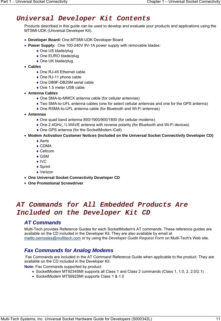
![Part 1 Universal Socket Connectivity Chapter 1 – Universal Socket Connectivity Multi-Tech Systems, Inc. Universal Socket Hardware Guide for Developers (S000342L) 10 Chapter 1 – Universal Socket Connectivity Multi-Tech Embedded Solutions Multi-Tech’s embedded device networking solutions instantly add communication ability to your existing or new product with minimal engineering effort giving you an edge on your competition while accelerating your time-to-market. Our universal socket family of embedded solutions is designed around a flexible comm-port architecture to provide analog dial-up, cellular, Wi-Fi or Bluetooth wireless, or Ethernet socket connectivity with interchangeable socket devices. This means you can utilize one system design and populate it with your preferred connectivity option giving you flexibility and a seamless migration path to future technologies. Universal Socket Connectivity Features Flexible comm-port architecture Interchangeable socket devices Cost-effective system design Easy migration to future technologies Complete global compliance The Universal Socket Design Each pin on a SocketModem corresponds to a particular function. The universal socket design provides a universal location for each function pin. This allows each SocketModem to be used in a common board. Comment [DAR2]: Saved as Universal SocketModem with pins.png 81KB saved in New graphics for K Comment [DAR3]: Pin Out_assignment_overview_fromDean_p5.png](https://usermanual.wiki/Multi-Tech-Systems/92U09G17825.User-Manual/User-Guide-1204041-Page-10.png)
![Part 1 Universal Socket Connectivity Chapter 1 – Universal Socket Connectivity Multi-Tech Systems, Inc. Universal Socket Hardware Guide for Developers (S000342L) 12 Universal Socket Pin Out Top View – Universal SocketModem Pin Out Universal Pin Descriptions Pin Signal Name In/Out Description 1 Tip I/O Tip Signal from Telco. Tip connection to the phone line (RJ-11 Pin 4). The SocketModem is Tip/Ring polarity insensitive. 2 Ring I/O Ring Signal from Telco. Ring connection to the phone line (RJ-11 Pin 3). The SocketModem is Tip/Ring polarity insensitive. 3 Safety Void NA Safety Clearance. 2.5 mm is required between TNV circuits and SELV circuits. 4 TX+ O Transmit Outputs (TX+ and TX-). Differential transmit outputs for Ethernet and ISDN. 5 TX- O Transmit Outputs (TX+ and TX-). Differential transmit outputs for Ethernet and ISDN. 6 RX- I Receive Inputs. Differential receive input pins for Ethernet. Dummy pin for MT810SWM-IP. 7 RX+ I Receive Inputs. Differential receive input pins for Ethernet. 8 Safety Void NA Safety Clearance. 2.5 mm is required between TNV circuits and SELV circuits. 9 Dummy Dummy pin for EDGE. 11 TCLK O Transmit Data Sync Clock. TX synchronous data clock for ISDN sync data mode. 12 RCLK O Receive Data Sync Clock. RX synchronous data clock for ISDN sync data mode. 22 MIC+ I Microphone positive input. See microphone sections in GPRS, CDMA, EDGE chapters. 23 MIC- I Microphone negative input. See microphone sections in GPRS, CDMA, EDGE chapters. Comment [DAR4]: Pin Out_Universal_July_2008_p14..png & FH9 7/14/08 Comment [DAR5]: SocketModem Uiversal Pinout flat view. png -- saved in Graphics new in Rev K -- 50 KB](https://usermanual.wiki/Multi-Tech-Systems/92U09G17825.User-Manual/User-Guide-1204041-Page-12.png)
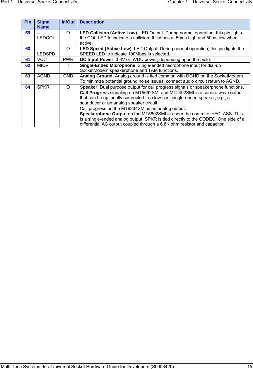
![Part 1 Universal Socket Connectivity Chapter 1 – Universal Socket Connectivity Multi-Tech Systems, Inc. Universal Socket Hardware Guide for Developers (S000342L) 13 Pin Signal Name In/Out Description 24 –RESET* I Device Reset (with pull-up). The active low –RESET input resets the device logic and returns the configuration of the device to the original factory default values or "stored values" in the NVRAM. –RESET is tied to VCC through a time-constant circuit for “Power-on-Reset” functionality. The SocketModem is ready to accept commands after a fixed amount of time (“X” Time) after power-on or reset. Model Time Constant "X" Time Minimum Reset Pulse* MTSMC-G2 250 ms 6 seconds 100us MTSMC-C1 250 ms 3-15 seconds 500us MTSMC-E1 250 ms 3-15 seconds 500us MTSMC-H 250 ms 10 seconds 100us MT9234SMI 400 ms 6 seconds 100us MT5692SMI 250 ms 6 seconds 100us MT2492SMI 250 ms 6 seconds 100us MT100SEM-IP 250 ms 6 seconds 100us MT810SWM-IP 250 ms 6 seconds 100us MTS2BTSMI 250 ms 6 seconds 100us *The SocketModem device may respond to a shorter reset pulse. Reset Line Interface for the MT5692SMI. The modem’s reset line employs a 10K pull up resistor. If an open collector driver is to be used, run that output to the modem only and use a separate driver for other embedded components. The modem’s reset signal may also be driven by a circuit that both sinks and sources current if desired. It is also important to note that these modems do not require an external reset. They have their own internal reset circuitry and voltage monitor and will function correctly even if the reset input is open. Reset GPRS and CDMA (MTSMC-G2 and MTSMC-C1). This signal is used to force a reset procedure by providing low level during reset of at least 500us. The signal is considered an emergency reset only. A reset procedure is already driven by internal hardware during the power-up sequence. If no external reset is necessary, this input can be left open. If used (emergency reset), it has to be driven by an open collector or an open drain. Reset EDGE with pull-up (MTSMC-E1). The active low –RESET input resets the device logic and returns the configuration of the device to the original factory default values of "stored values" in the NVRAM. The SocketModem is ready to accept commands after a fixed amount of time after power-on or reset. 25 USB_VBUS I USB Voltage Sense. Senses the voltage level of the USB to determine if the bus is available. 26 GND GND Logic Ground. 27 USB_DP I/O USB Data Positive. Positive pin of the USB data pair. 28 USB_DN I/O USB Data Negative. Negative pin of the USB data pair. 29 LED DCD O DCD (Active High). Output from 74LCX14 with a 1000 Ohms resistor in series. SocketWireless Bluetooth (MTS2BTSMI): When lit, indicates a connection. No series resistor. 30 LED RX O RX (Active High). Output from 74LCX14 with a 1000 Ohms resistor in series. SocketWireless Bluetooth (MTS2BTSMI): No series resistor. 31 LED DTR O DTR (Active High). Output from 74LCX14 with a 1000 Ohms resistor in series. SocketWireless Bluetooth (MTS2BTSMI): No series resistor. 32 LED TX O TX (Active High). Output from 74LCX14 with a 1000 Ohms resistor in series. SocketWireless Bluetooth (MTS2BTSMI): No series resistor. 33 –RTS I Request to Send (Active Low). –RTS is controlled by the DTE to indicated whether or not the DTE is ready to receive data. –RTS ON (low) indicates that the DTE is ready to receive data from the modem on RXD. –RTS OFF indicates to the SocketModem that it should not transfer data on the RXD. In the command state, the modem ignores –RTS. Note: When the –RTS pin is not in use, it should be tied low. * RESET – A Design Consideration: Allowing the host processor to control the RESET line of the SocketModem provides the benefit of allowing the host to reset the device in the event of a failure to respond normally. Resetting the SocketModem will return it to a known functional state. Comment [DAR6]: For all builds --Dustin 8/24/09 Comment [DAR7]: New from Tim Gunn 07/14/09Comment [DAR8]: Bud wondered if this text is for E1 too (it was used with initial EDGE). It’s in the section that describes the pin functionality. 9/8/09 review: Reset EDGE with pull-up (MTSMC-E1). Dustin's answer Original edge documentation is incorrect. You could probably remove: –RESET is tied to VCC through a time-constant circuit for “Power-on-Reset” functionality.](https://usermanual.wiki/Multi-Tech-Systems/92U09G17825.User-Manual/User-Guide-1204041-Page-13.png)
![Part 1 Universal Socket Connectivity Chapter 1 – Universal Socket Connectivity Multi-Tech Systems, Inc. Universal Socket Hardware Guide for Developers (S000342L) 18 Mechanical Drawing in Inches for the Listed Products Comment [DAR9]: Mechanical Drawing for Analog Modems from Dean 4-16-09.png](https://usermanual.wiki/Multi-Tech-Systems/92U09G17825.User-Manual/User-Guide-1204041-Page-18.png)
![Part 1 Universal Socket Connectivity Chapter 1 – Universal Socket Connectivity Multi-Tech Systems, Inc. Universal Socket Hardware Guide for Developers (S000342L) 19 Mechanical Drawing in Millimeters for Listed Products Comment [DAR10]: Mechanical Drawing for Analog Modems-Metric from Dean 4-16-09.png](https://usermanual.wiki/Multi-Tech-Systems/92U09G17825.User-Manual/User-Guide-1204041-Page-19.png)
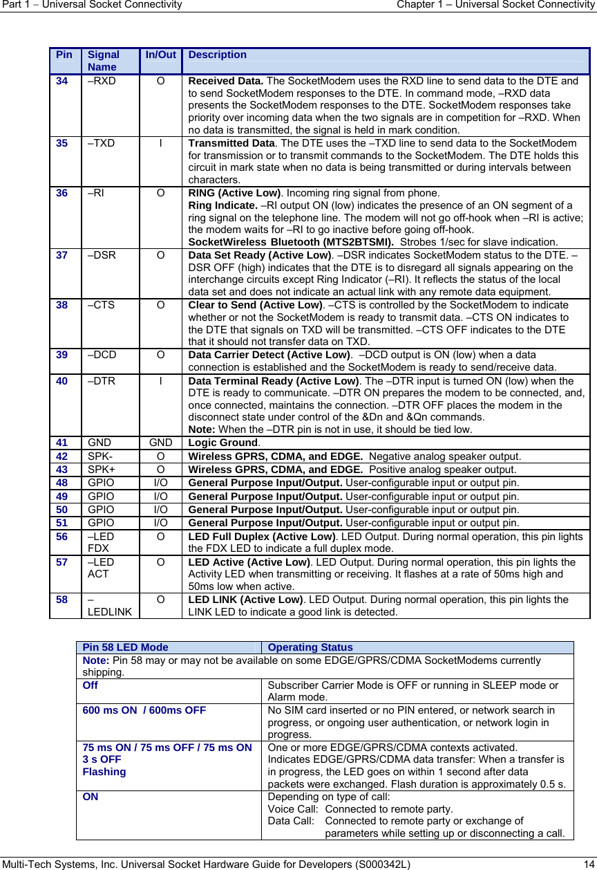
![Part 1 Universal Socket Connectivity Chapter 1 – Universal Socket Connectivity Multi-Tech Systems, Inc. Universal Socket Hardware Guide for Developers (S000342L) 21 SocketModem Developer Board This developer board drawing shows the major board components for all SocketModems. Board Revision B See the next page for description of Board Components Comment [DAR11]: Board B for Universal 260b0_forRev J jumper fixed 2 29grayscale50percent.gif done 8/5/09](https://usermanual.wiki/Multi-Tech-Systems/92U09G17825.User-Manual/User-Guide-1204041-Page-21.png)
![Part 1 Universal Socket Connectivity Chapter 1 – Universal Socket Connectivity Multi-Tech Systems, Inc. Universal Socket Hardware Guide for Developers (S000342L) 23 SocketModem Developer Board Block Diagram Comment [DAR12]: C:\ Universal SocketModem\Graphics ETC Rev I\Block diagram board B\Block diagram board B w antenna.png. 38 KB](https://usermanual.wiki/Multi-Tech-Systems/92U09G17825.User-Manual/User-Guide-1204041-Page-23.png)
![Part 1 Universal Socket Connectivity Chapter 1 – Universal Socket Connectivity Multi-Tech Systems, Inc. Universal Socket Hardware Guide for Developers (S000342L) 24 Developer Board Schematics Board Revision B Comment [DAR13]: Schematics Board B page 2 Scan0576_000.jpg did not change to gif -- file was already small](https://usermanual.wiki/Multi-Tech-Systems/92U09G17825.User-Manual/User-Guide-1204041-Page-24.png)
![Part 1 Universal Socket Connectivity Chapter 1 – Universal Socket Connectivity Multi-Tech Systems, Inc. Universal Socket Hardware Guide for Developers (S000342L) 26 Board Revision B Developer Board Schematics Board Revision B Comment [DAR14]: Schematics Board B page 3 Scan0577_000 grayscale50percent.gif (changed from jpg to make the file size smaller 8/5/09) Comment [DAR15]: Schematics Board B page 4 Scan0575_000grayscale.gif (was jpg - now a gif for a smaller file 8/5/09](https://usermanual.wiki/Multi-Tech-Systems/92U09G17825.User-Manual/User-Guide-1204041-Page-26.png)
![Part 1 Universal Socket Connectivity Chapter 1 – Universal Socket Connectivity Multi-Tech Systems, Inc. Universal Socket Hardware Guide for Developers (S000342L) 27 Developer Board Schematics Board Revision B Comment [DAR16]: Schmatics Board B page 5 Scan0574_000grayscale50percent.gif (was jpg but file was too large. Now gif 8/5/09)](https://usermanual.wiki/Multi-Tech-Systems/92U09G17825.User-Manual/User-Guide-1204041-Page-27.png)
![Part 1 Universal Socket Connectivity Chapter 1 – Universal Socket Connectivity Multi-Tech Systems, Inc. Universal Socket Hardware Guide for Developers (S000342L) 28 Developer Board Schematics Board Revision B Comment [DAR17]: Schematics Board B page 6 Scan0573_000.jpg did not change to gif -- file was aleady small](https://usermanual.wiki/Multi-Tech-Systems/92U09G17825.User-Manual/User-Guide-1204041-Page-28.png)
![Part 1 Universal Socket Connectivity Chapter 1 – Universal Socket Connectivity Multi-Tech Systems, Inc. Universal Socket Hardware Guide for Developers (S000342L) 30 XMODEM Serial Port Upgrade This upgrade procedure applies only to the MT810SWM-IP and the older product MTXCSEM. The IP communications device, for example, contains a 2 MB flash wherein the boot image, the firmware and configuration files are stored in a compressed format. The flash can easily be upgraded both locally as well as remotely. Serial Port Upgrade The flash of the can be upgraded locally through serial port using the upload feature of serial applications. Serial Port Configuration The default serial port parameters should be: Data length – 8 bits Parity – None Stop bits – 1 Baud-rate of the serial port to which the communications device is connected should be set to 115200 bps for proper operation. Example of a Serial Flash Upgrade Following steps explain the procedure to upgrade a flash using the serial COM port (serial flash upgrade). Connect the communications device to a PC COM Port. Open an application through which we can access the serial device (e.g., Meterm, zoc, hyperterm). Reboot the communications device. Wait for the boot message and prompt “press d to download” to appear. Press d when prompted. Select the XMODEM Protocol from the Terminal application. Choose a file to be uploaded. Perform a file upload. The communications device reboots and will be up after a few seconds (10-15 seconds). Caution: Refrain from powering off the device during flash upgrade.Comment [DAR18]: Removed all direct references to the SocketEthernet IP. Kevin said this applies to these 2 products 8/09 Comment [DAR19]: Removed "TFTP Ethernet Upgrade" section. Darrick said it applied only to the MTXCSEM which this manual no longer covers.](https://usermanual.wiki/Multi-Tech-Systems/92U09G17825.User-Manual/User-Guide-1204041-Page-30.png)
![Part 1 Universal Socket Connectivity Chapter 1 – Universal Socket Connectivity Multi-Tech Systems, Inc. Universal Socket Hardware Guide for Developers (S000342L) 31 Multi-Tech Systems, Inc. Flash Programming Protocol This information is provided exclusively for the users of Multi-Tech Systems, Inc. SocketModems, specifically the MT9234SMI. Multi-Tech Systems, Inc. SocketModem owners have the right to use, modify, and incorporate this code into other products provided they include the Multi-Tech Systems, Inc. notice and the associated copyright notice with any such product. Copyright (C) Multi-Tech Systems, Inc. 1995 All Right Reserved The flash programming protocol is provided "AS IS” without warranty. Important: When interacting with the boot code, it is possible to make the modem inoperable. Use extreme caution. Programming the Modem There are two ways to start flash programming a modem. It can be programmed 1. From “AT” mode 2. When the modem powers up. The following table shows how a modem is programmed. DTE Modem Comments AT*FS\r This effectively “restarts” the modem so that it enters the boot code. Handshake Sequence M’s Many M’s are sent (10 milliseconds apart) at 19200 baud. This is where the handshake starts if the modem is just powered up. U U is sent at 19200 baud if M’s are received within 100 milliseconds of power up. If the M’s are not received within 100 milliseconds, then the modem starts up normally. If the AT*FS command is used, then you have 1 second (1000mS) to perform the handshake. D Sent at 19200 baud. M M if can receive at 9600/19200/38400/57600/115200 I|J|K|L|M I if modem will be programmed at 9600 J if modem will be programmed at 19200 K if modem will be programmed at 38400 L if modem will be programmed at 57600 M if modem will be programmed at 115200 \r\nOK\r\n Modem is ready to be programmed Program Sequence: DTE Modem Comments ATFLP\r Request to the modem to program G Modem is ready for next program packet [Length High] High byte of data packet length [Length Low] Low byte of data packet length Packet lengths can be up to 4096 bytes in size for most boot code versions [Address High] High byte of program address [Address Middle] Middle byte of program address [Address Low] Low byte of program address Addresses are 3 byte values with a range of 00000h-FFFFFh [Data Bytes] These are the data bytes to be programmed at the address specified above. They must be the same number of bytes as specified above. [Checksum] This checksum is generated by exclusive ORing together all of the Data Bytes (do not include the Length or Address bytes in that calculation). \nOK\r\n \nERROR\r\n If bytes are programmed and verified. If verify fails or checksum is bad. Retry the block 3 times on an ERROR. …. …. More of the above sequence until all the data bytes have been sent to the modem. ATFLEND\r This ends programming and restarts the modem.](https://usermanual.wiki/Multi-Tech-Systems/92U09G17825.User-Manual/User-Guide-1204041-Page-31.png)
![Part 1 Universal Socket Connectivity Chapter 1 – Universal Socket Connectivity Multi-Tech Systems, Inc. Universal Socket Hardware Guide for Developers (S000342L) 35 Coax Cables MMCX-to-SMA and MMCX to RSMA Coax Cable This cable shown below is included in the Developer Kit for the CDMA, EDGE SocketModems, and the SocketWireless Bluetooth. Cable Specifications Cable Type: Coax Cable Attenuation: <1.0db Connector Impedance: 50 Ohms An optional antenna cable (SMA to MMCX) can be ordered from Multi-Tech Systems, Inc. Part Number Description CASMA-MMCX-1 SMA to MMCX COAX RF 6 inch cable (Single Pack) CASMA-MMCX-10 SMA to MMCX COAX RF 6 inch cable (Ten Pack) MMCX-to-SMA Adapter An antenna with an SMA connector may be directly connected to a SocketModem GPRS/CDMA through a mating MMCX-to-SMA adapter. SMA-to-MMCX Connector Available from Amphenol Amphenol http://www.amphenol.com/ Order No: 908-31100 Comment [DAR20]: Adapter_Amphenol.gif Comment [DAR21]: Now new from Dean. (was Wireless Antenna Cable from Ken 20903C_cable only.jpg Wireless Antenna Cable from Ken_20903c_generic.FH9f Wireless Antenna Cable from Ken_20903c_generic.pdf)](https://usermanual.wiki/Multi-Tech-Systems/92U09G17825.User-Manual/User-Guide-1204041-Page-35.png)
![Part 1 Universal Socket Connectivity Chapter 1 – Universal Socket Connectivity Multi-Tech Systems, Inc. Universal Socket Hardware Guide for Developers (S000342L) 36 UFL-to-SMA and UFL-to-RSMA Coax Cable The UFL-to-SMA cable is included in the Developer Kit for the GPS (Global Positioning), GPRS and HSDPA SocketModems. Cable Specifications Cable Type: Coaxial Cable Attenuation: <1.0db Connector Impedance: 50 ohm An optional antenna cables can be ordered from Multi-Tech Systems, Inc. Part Number Description CASMA8-UFL-1 SMA to UFL COAX RF 8 inch cable (Single Pack) CASMA8-UFL-10 SMA to UFL COAX RF 8 inch cable (Ten Pack) CARSMA8-UFL-1 RSMA to UFL COAX RF 8 inch cable (Single Pack) CARSMA8-UFL-10 RSMA to UFL COAX RF 8 inch cable (Ten Pack) PTCRB Requirements for the Antenna There cannot be any alteration to the authorized antenna system. The antenna system must be the same type with similar in-band and out-of-band radiation patterns and maintain the same specifications. FCC Requirements for the Antenna The antenna gain, including cable loss, must not exceed 3.0 dBi at 1900 MHz / 1.6 dBi at 850 MHz for mobile operating and fixed mounted operations, as defined in 2.1091 and 1.1307 of the rules for satisfying RF exposure compliance. Comment [DAR22]: Now new from Dean SocketModem_SS_Auxiliary Cable. PNG 2/4/2009](https://usermanual.wiki/Multi-Tech-Systems/92U09G17825.User-Manual/User-Guide-1204041-Page-36.png)
![Part 1 Universal Socket Connectivity Chapter 1 – Universal Socket Connectivity Multi-Tech Systems, Inc. Universal Socket Hardware Guide for Developers (S000342L) 37 Account Activation for Wireless Devices Pre-Configured Multi-Tech Products Some Multi-Tech wireless modems have been pre-configured to operate on a specific wireless network, such as Sprint and Verizon. However, before you can begin to use the modem, you must set up a wireless data account with your wireless network provider. Then, follow the activation procedures covered on the Activation Notices available from Multi-Tech. Wireless Approvals and Labeling Requirements Approvals and Certification The Multi-Tech SocketModem is Industry and/or Carrier Approved as an End Product modem. In most cases, when integrated and used with an antenna system that was part of the Multi-Tech modem certification, no additional approvals or certifications are required (however, CDMA has a few exceptions) for the device you develop as long as the following are met: PTCRB Requirements: The antenna system cannot be altered. Model Identification: IMPORTANT When the wireless carrier asks you to provide the modem's model identification, give the Multi-Tech wireless model identification, not the identification of the host device model. See the label example below. The Multi-Tech model identification allows the carrier to verify the modem as one of its approved models. This information is located on the modem's label. The Following Is an Example of an End Product GPRS Label: Host Device Model Identification Multi-Tech SocketModem Model Identification IMEI (International Mobile Equipment Identity) Comment [DAR23]: Now Label F4.png saved in Graphics new in Rev K 62kb](https://usermanual.wiki/Multi-Tech-Systems/92U09G17825.User-Manual/User-Guide-1204041-Page-37.png)
![Part 1 Universal Socket Connectivity Chapter 1 – Universal Socket Connectivity Multi-Tech Systems, Inc. Universal Socket Hardware Guide for Developers (S000342L) 38 The Following Is an Example of an End Product CDMA Label: Multi-Tech Model Identification Multi-Tech Ordering Part Number ESN: Electronic Serial Number in Hexadecimal Format and Decimal Format Other Information the Wireless Carrier Asks You to Provide: For CDMA SocketModems: The modem's 8-character ESN (Electronic Serial Number) number printed next to the barcode on the modem. The ESN may vary in format by various CDMA carriers; some use a decimal number while others use a hexadecimal number. For GSM SocketModems: The modem's 15-character IMEI (International Mobile Equipment Identity) number printed on the modem's label. Comment [DAR24]: Label Small-C.png 23KB 6/16/09](https://usermanual.wiki/Multi-Tech-Systems/92U09G17825.User-Manual/User-Guide-1204041-Page-38.png)
![Part 1 Universal Socket Connectivity Chapter 1 – Universal Socket Connectivity Multi-Tech Systems, Inc. Universal Socket Hardware Guide for Developers (S000342L) 42 Label Examples for Analog SocketModems Note: These do not apply to the Wireless GPRS and CDMA products. Serial Label This label shows the modem model (M/N), build option (B/O), date of manufacture (DOM), serial number, and North America and European Union regulatory information. This is an example of Regulatory Label which is available from Multi-Tech by request. Comment [DAR25]: Label Small MT9234SMI.png 6/16/09 Label 9234SMI Scan0549_000.png 6/16/09 Comment [DAR26]: Label 9234SMI Scan 0549_000.png 55KB 6/15/09](https://usermanual.wiki/Multi-Tech-Systems/92U09G17825.User-Manual/User-Guide-1204041-Page-42.png)
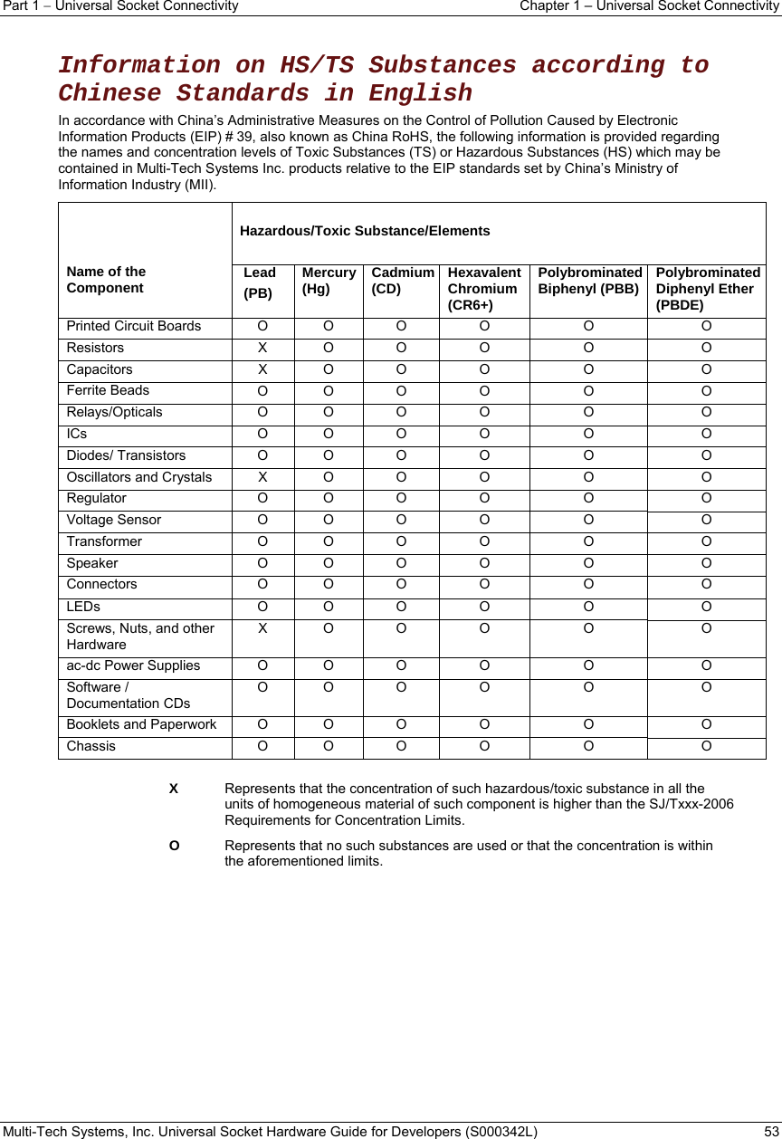
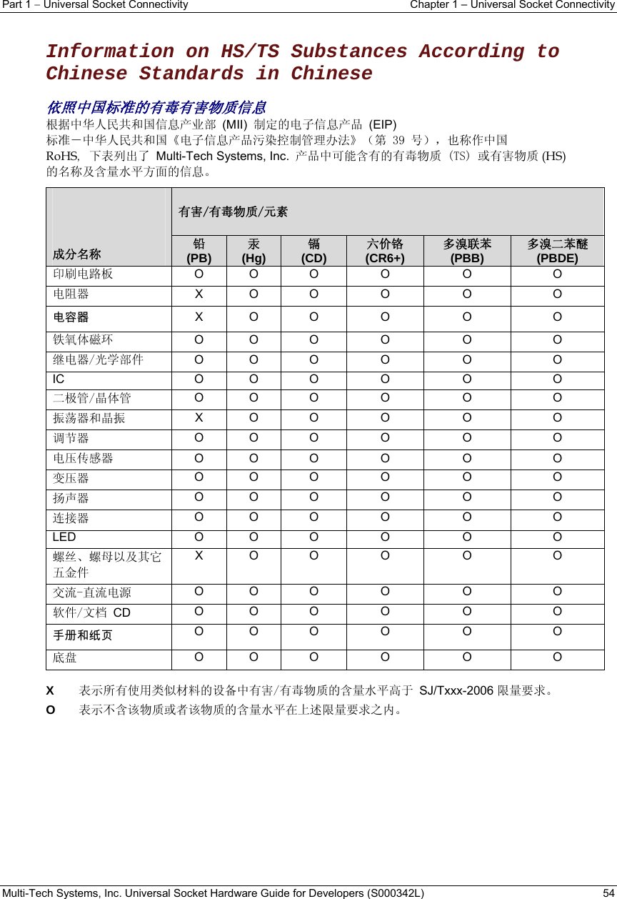
![Part 1 Universal Socket Connectivity Chapter 1 – Universal Socket Connectivity Multi-Tech Systems, Inc. Universal Socket Hardware Guide for Developers (S000342L) 52 Restriction of the Use of Hazardous Substances (RoHS) Multi-Tech Systems, Inc. Certificate of Compliance 2002/95/EC Multi-Tech Systems Inc. confirms that its embedded products now comply with the chemical concentration limitations set forth in the directive 2002/95/EC of the European Parliament (Restriction Of the use of certain Hazardous Substances in electrical and electronic equipment - RoHS) These Multi-Tech Systems, Inc. products do not contain the following banned chemicals: Lead, [Pb] < 1000 PPM Mercury, [Hg] < 1000 PPM Hexavalent Chromium, [Cr+6] < 1000 PPM Cadmium, [Cd] < 100 PPM Polybrominated Biphenyl, [PBB] < 1000 PPM Polybrominated Diphenyl Ether, [PBDE] < 1000 PPM Moisture Sensitivity Level (MSL) =1 Maximum Soldering temperature = 260C (wave only) Notes: 1. Lead usage in some components is exempted by the following RoHS annex; therefore, higher lead concentration would be found in some SocketModems (>1000ppm). a. Lead in high melting temperature type solders (i.e., tin-lead solder alloys containing more than 85% lead). b. Lead in electronic ceramic parts (e.g., piezoelectronic devices). 2. Moisture Sensitivity Level (MSL) – Analysis is based on the components/material used on the board. Comment [DAR27]: Stored in common text as png. 3KB Comment [DAR28]: Bud said to take out the Tin Whisker growth statements 8/24/09. He had said this previously, but they somehow didn't get removed.](https://usermanual.wiki/Multi-Tech-Systems/92U09G17825.User-Manual/User-Guide-1204041-Page-52.png)
![PART 2 – Embedded Wireless Modems Chapter 2 – SocketModem Cell and iCell Multi-Tech Systems, Inc. Universal Socket Hardware Guide for Developers (S000342L) 57 Technical Specifications The MTSMC-G2 and MTSMC-G2-IP SocketModems meet the following specifications: Category Description Standards GPRS Class 10 Frequency Bands Quad-band GSM/EGPRS 850/900/1800/1900 MHz Serial/Data Speed Serial interface supports DTE speeds up to 921.6K IP interface supports DTE speeds at the fixed rate of 115.2 Packet data up to 85.6K bps Circuit-switched data (GPRS) up to 14.4K bps transparent and non-transparent Supports data rates of 921600, 460800, 230400, 115200 bps Data Format 10 bit Serial Asynchronous Data Error Correction MNP2 Data Compression V.42bis Weight 1 oz. (28 g) Size 3.15" x 1.375" (80.010 mm x 34.925 mm) Operating Temperature -40° C to +85° C Storage Temperature -40 °C to +85°C Humidity 10% to 90% Input Power 5VDC Operating Voltage Supply Range: VCC Maximum: 5.5 Voltage at Any Signal Pin Minimum: GND Maximum: VCC Antenna Connector Surface mount UFL SIM Holder Standard 3V SIM holder IP Protocols Supported MTSMC-G2 DNS Resolve, FTP client, LCP, PPP (dial-out),TCP socket, UDP socket, PAP & CHAP authentication MTSMC-G2-IP DNS Client, FTP Client, ICMP (Ping), POP3 Client, SMTP Client, TCP Client & Server, UDP Client & Server, IP, PPP (dial-out) with PAP & CHAP authentication M2M Applications MTSMC-G2-IP Automatic connect/reconnect, device monitor, modem emulation, Ping & TCP keep alive, wake-up on caller ID, wake-up on ring Compliance EMC Compliance FCC Part 15 EN55022 EN55024 Radio Compliance FCC Part 22 FCC Part 24 RSS 132 RSS 133 EN 301 511 EN 301 489-1 EN 301 489-7 AS/ACIF S042.1 AS/ACIF S042.3 Safety Compliance UL 60950-1 cUL 60950-1 IEC 60950-1 AS/NZS 60950-1 Network Compliance PTCRB Warranty Two years Comment [DAR29]: From Dustin 6/24/09Comment [DAR30]: From Dustin 6/24/09 Comment [DAR31]: Updated list from Dustin for Rev. K](https://usermanual.wiki/Multi-Tech-Systems/92U09G17825.User-Manual/User-Guide-1204041-Page-57.png)
![PART 2 – Embedded Wireless Modems Chapter 2 – SocketModem Cell and iCell Multi-Tech Systems, Inc. Universal Socket Hardware Guide for Developers (S000342L) 58 Specifications Continued: Category Description Features Modes of Operation: Data Mode, Command Mode, and Voice Mode Embedded TCP/IP stack Short Message Services (SMS) RTS/CTS hardware flow control AT command compatible Support for HR, FR, EFR, and AMR (Adaptive Multi Rate) voice codec support Flash upgradeable Non-volatile memory DC Electrical Characteristics Units: Volts 5V DC Characteristics (VDD = 5V ± 0.25V) VDDMAX = 5.25V Parameter Minimum Maximum Digital Signal Input Low Level –DTR (40), –TXD (35), –RTS (33) GND 0.8 Digital Signal Input High Level –DTR (40), –TXD (35), –RTS (33) 2 Vcc Digital Signal Output Low Level –DCD (39), –CTS (38), –DSR (37), –RI (36), –RXD (34) 0.4 Digital Signal Output High Level –DCD (39), –CTS (38), –DSR (37), –RI (36), –RXD (34) 3.84 Reset (Low Active) Input Low Level –Reset (24) 0.8 Reset (Low Active) Input High Level –Reset (24) 2 Digital Input Capacitance 14pF Power Measurements MTSMC-G2 Measured Power* Measures at Input Voltage 5.00 Sleep Typical Maximum Peak Current (AMPS) 0.049 0.113 0.24 1.10 Watts 0.245 0.564 1.195 MTSMC-G2-IP Measured Power* Measures at Input Voltage 5.00 Sleep Typical Maximum Peak Current (AMPS) 0.080 0.135 0.280 1.250 Watts 0.382 0.664 1.358 Note: Current Peak = 1500mA maximum during Tx burst. MTSMC-G2-GP (for GPS) Measured Power* Measures at Input Voltage 5.00 Sleep Mode Typical Maximum Peak Current (AMPS) 0.013 0.115 0.481 1.400 Watts 0.065 0.574 2.386 Comment [DAR32]: Measurements for MTSMC-G2-IP 73120965 Rev 0 from Tom Fix. He suggested the current peak text also 4/22/09. He said these measurements apply to G2 without IP, too. Comment [DAR33]: Measurements for MTSMC-G2-IP 73120965 Rev 0 from Tom Fix. He suggested the current peak text also 4/22/09. He said these measurements apply to G2 without IP, too. Comment [DAR34]: Measurements for MTSMC-G2-gp from Tom Fix 10/06/09.](https://usermanual.wiki/Multi-Tech-Systems/92U09G17825.User-Manual/User-Guide-1204041-Page-58.png)

![PART 2 – Embedded Wireless Modems Chapter 2 – SocketModem Cell and iCell Multi-Tech Systems, Inc. Universal Socket Hardware Guide for Developers (S000342L) 60 Mechanical Drawings – Basic Build Comment [DAR35]: Vault Data 357 08/26/09](https://usermanual.wiki/Multi-Tech-Systems/92U09G17825.User-Manual/User-Guide-1204041-Page-60.png)
![PART 2 – Embedded Wireless Modems Chapter 2 – SocketModem Cell and iCell Multi-Tech Systems, Inc. Universal Socket Hardware Guide for Developers (S000342L) 61 Mechanical Drawings – Voice Build Comment [DAR36]: Vault Data 375 08/26/09](https://usermanual.wiki/Multi-Tech-Systems/92U09G17825.User-Manual/User-Guide-1204041-Page-61.png)
![PART 2 – Embedded Wireless Modems Chapter 2 – SocketModem Cell and iCell Multi-Tech Systems, Inc. Universal Socket Hardware Guide for Developers (S000342L) 62 Mechanical Drawings – IP Build Comment [DAR37]: 8/26/09. Dean's #357 in Vault Data MTSMC-G2-IP-Manual.png](https://usermanual.wiki/Multi-Tech-Systems/92U09G17825.User-Manual/User-Guide-1204041-Page-62.png)
![PART 2 – Embedded Wireless Modems Chapter 2 – SocketModem Cell and iCell Multi-Tech Systems, Inc. Universal Socket Hardware Guide for Developers (S000342L) 63 Mechanical Drawings – GPS Build Comment [DAR38]: 8/26/09. Dean's #357 in Vault Data MTSMC-G2-GP-Manual.png](https://usermanual.wiki/Multi-Tech-Systems/92U09G17825.User-Manual/User-Guide-1204041-Page-63.png)
![PART 2 – Embedded Wireless Modems Chapter 2 – SocketModem Cell and iCell Multi-Tech Systems, Inc. Universal Socket Hardware Guide for Developers (S000342L) 64 Application Notes Flashing LED Interface The flashing LED signal is used to indicate the working mode of the SocketModem. LEDs and SocketModem Status Signal SocketModem Status OFF Download mode or switched OFF> Continuously lit Switched ON (not registered on the network) ON Flashing Switched ON (registered on the network) RF Performances RF performances are compliant with the ETSI recommendation 05.05 and 11.10. Note: The following statistics are subject to change due to pending test results. The main parameters are: Receiver Features EGSM Sensitivity : < -104 dBm GSM 1800/GSM 1900 Sensitivity : < -102 dBm Selectivity @ 200 kHz : > +9 dBc Selectivity @ 400 kHz : > +41 dBc Dynamic range : 62 dB Intermodulation : > -43 dBm Co-channel rejection : + 9 dBc Transmitter Features Maximum output power (EGSM) : 33 dBm ± 2 dB Maximum output power (DCS/PCS) : 30 dBm ± 2 dB Minimum output power (EGSM): 5 dBm ± 5 dB Minimum output power (DCS/PCS): 0 dBm ± 5 dB H2 level : < -30 dBm H3 level : < -30 dBm Noise in 925 - 935 MHz : < -67 dBm Noise in 935 - 960 MHz : < -79 dBm Noise in 1805 - 1880 MHz : < -71 dBm Phase error at peak power : < 5 ° RMS Frequency error : ± 0.1 ppm max RF Connection and Antenna The RF connector on the SocketModem GPRS is a UFL standard type. See Chapter 1 for Antenna System details. Microphone Inputs The MIC inputs are differential ones. They already include the convenient biasing for an electret microphone (0.5 mA and 2 Volts). This electret microphone can be directly connected on these inputs. The impedance of the microphone has to be around 2K. These inputs are the standard ones for a handset design. The gain of the MIC inputs is internally adjusted. The gain can be tuned from 30dB to 51dB. The connection to the microphone is direct. MIC2NMIC2PC1C1 = 22pF to 100 pF33 pF recommended Comment [DAR39]: Tom Hofstedt expects text results in by June 24th.](https://usermanual.wiki/Multi-Tech-Systems/92U09G17825.User-Manual/User-Guide-1204041-Page-64.png)

![PART 2 – Embedded Wireless Modems Chapter 3 – SocketModem CDMA Multi-Tech Systems, Inc. Universal Socket Hardware Guide for Developers (S000342L) 70 Mechanical Drawings – Basic Build Comment [DAR40]: Vault Data #315 8/26//09](https://usermanual.wiki/Multi-Tech-Systems/92U09G17825.User-Manual/User-Guide-1204041-Page-70.png)
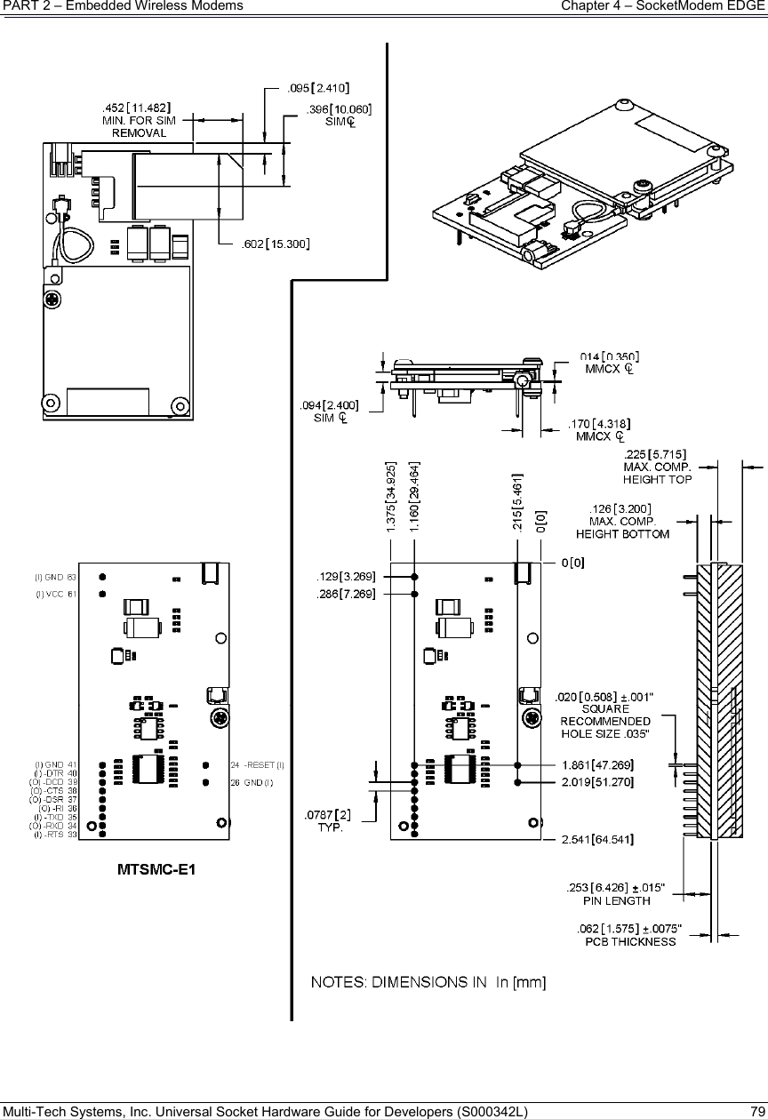
![PART 2 – Embedded Wireless Modems Chapter 4 – SocketModem EDGE Multi-Tech Systems, Inc. Universal Socket Hardware Guide for Developers (S000342L) 78 Mechanical Drawings – Basic Build Comment [DAR41]: Vault Data for E1 is #372 8/26/09](https://usermanual.wiki/Multi-Tech-Systems/92U09G17825.User-Manual/User-Guide-1204041-Page-78.png)
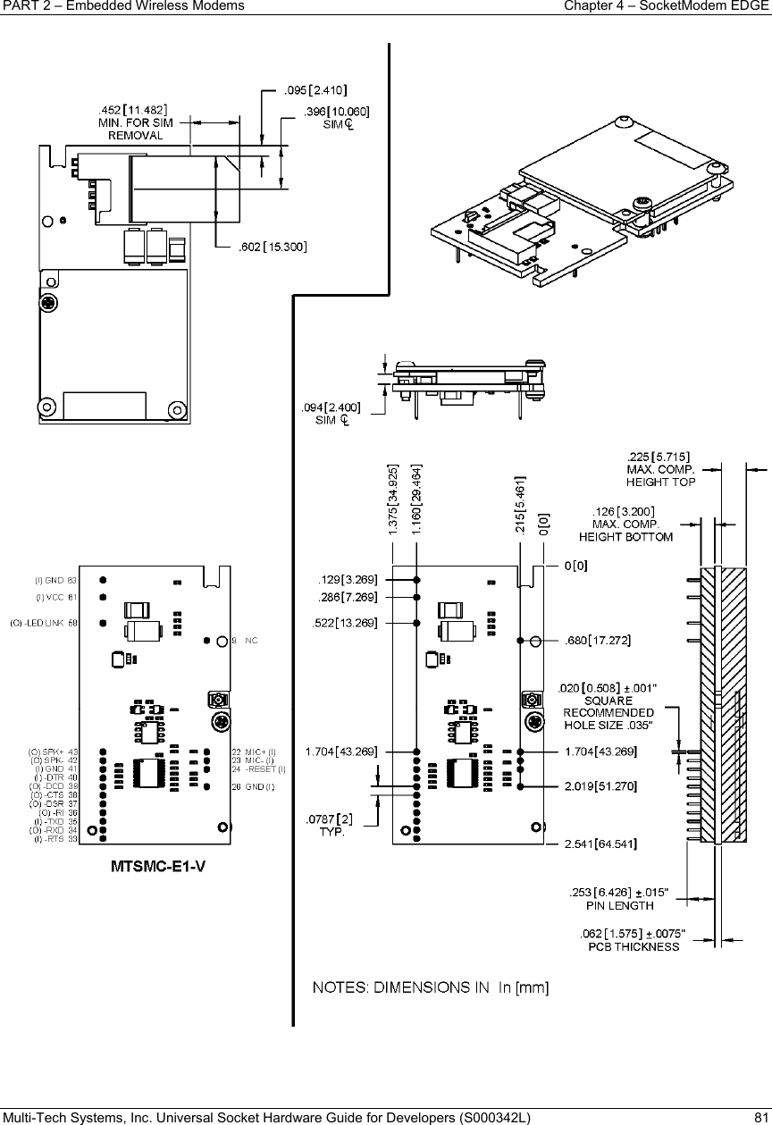
![PART 2 – Embedded Wireless Modems Chapter 4 – SocketModem EDGE Multi-Tech Systems, Inc. Universal Socket Hardware Guide for Developers (S000342L) 80 Mechanical Drawings – Voice Build Comment [DAR42]: Vault Data for E1 Voice is #372 8/26/09](https://usermanual.wiki/Multi-Tech-Systems/92U09G17825.User-Manual/User-Guide-1204041-Page-80.png)
![PART 2 – Embedded Wireless Modems Chapter 4 – SocketModem EDGE Multi-Tech Systems, Inc. Universal Socket Hardware Guide for Developers (S000342L) 82 DC Electrical Characteristics Operating Conditions 5 Volts Parameter Minimum Maximum Supply Range - Vcc 4.75 5.25 Absolute Maximum Rating Parameter Minimum Maximum Voltage at Any Signal Pin 0 5 DC Electrical Characteristics Units (Volts) Parameter Minimum Maximum 0 0.8 Digital Signal Input Low Level 2 5 Digital Signal Input High Level 0 0.33 Digital Signal Output Low Level 3.84 5 Digital Signal Output High Level 0 1.14 Reset (Low Active) Input Low 2.7 5 Reset (Low Active) Input High Digital Input Capacitance 10pF Power Measurements MTSMC-E1 and MTSMC-E1-V Measured Power* at Input Voltage 5.00 Sleep Typical Maximum Peak Current (AMPS) 0.010 0.128 0.675 1.500 Watts 0.050 0.64 3.2 * Multi-Tech Systems, Inc. recommends that the customer incorporate a 10% buffer into their power source when determining product load. Comment [DAR43]: New from Dustin 8/31/09 for E1 Comment [DAR44]: These measurements apply to both the MTSMC-E1 and MTSMC-E1-V since the only difference is the voice pins.From Jerome 9/8/09](https://usermanual.wiki/Multi-Tech-Systems/92U09G17825.User-Manual/User-Guide-1204041-Page-82.png)
![PART 2 – Embedded Wireless Modems Chapter 5 – SocketModem HSDPA Multi-Tech Systems, Inc. Universal Socket Hardware Guide for Developers (S000342L) 85 Technical Specifications The SocketModem HSDPA (MTSMC- H) wireless modem meets the following specifications: Category Description General Frequency Bands • UMTS/HSDPA: Triple band, 850/1900/2100MHz • GSM/GPRS/EDGE: Quad band, 850/900/1800/1900MHz GSM Class Small MS Output power (according to Release 99) Class 4 (+33dBm ±2dB) for EGSM850 Class 4 (+33dBm ±2dB) for EGSM900 Class 1 (+30dBm ±2dB) for GSM1800 Class 1 (+30dBm ±2dB) for GSM1900 Class E2 (+27dBm ± 3dB) for GSM 850 8-PSK Class E2 (+27dBm ± 3dB) for GSM 900 8-PSK Class E2 (+26dBm +3 /-4dB) for GSM 1800 8-PSK Class E2 (+26dBm +3 /-4dB) for GSM 1900 8-PSK Class 3 (+24dBm +1/-3dB) for UMTS 2100, WCDMA FDD BdI Class 3 (+24dBm +1/-3dB) for UMTS 1900,WCDMA FDD BdII Class 3 (+24dBm +1/-3dB) for UMTS 850, WCDMA FDD BdV Power Supply 5VDC 10% Physical Description 3.1" L x 1.4" W x 0.5" H; 1 oz. (7.8 cm x 3.5 cm x 1.2 cm; 28 g) HSDPA Features 3GPP Release 5 3.6 Mbps, UL 384 kbps UE CAT. [1-6], 11, 12 supported Compressed mode (CM) supported according to 3GPP TS25.212 UMTS Features 3GPP Release 4 PS data rate – 384 kbps DL / 384 kbps UL CS data rate – 64 kbps DL / 64 kbps UL GSM / GPRS / EGPRS Features Data Transfer GPRS • Multislot Class 10 • Full PBCCH support • Mobile Station Class B • Coding Scheme 1 – 4 EGPRS • EDGE E2 power class for 8 PSK • Downlink coding schemes – CS 1-4, MCS 1-9 • Uplink coding schemes – CS 1-4, MCS 1-9 • BEP reporting • SRB loopback and test mode B • 8-bit, 11-bit RACH • PBCCH support • 1 phase/2 phase access procedures • Link adaptation and IR • NACC, extended UL TBF • Mobile Station Class B CSD • V.110, RLP, non-transparent • 9.6 kbps SMS Point-to-point MT and MO Cell broadcast Text and PDU mode Software AT Commands AT GSM 07.05 and 07.07, Siemens AT commands for RIL compatibility (NDIS/RIL) Microsoft Compatibility RIL / NDIS for Windows Mobile® SIM Application Toolkit SAT Class C Firmware Update Firmware update from host application over USB and ASC0](https://usermanual.wiki/Multi-Tech-Systems/92U09G17825.User-Manual/User-Guide-1204041-Page-85.png)
![PART 2 – Embedded Wireless Modems Chapter 5 – SocketModem HSDPA Multi-Tech Systems, Inc. Universal Socket Hardware Guide for Developers (S000342L) 87 Mechanical Drawings – Basic Build Comment [DAR45]: Vault Data #319 for basic build 8/26/09](https://usermanual.wiki/Multi-Tech-Systems/92U09G17825.User-Manual/User-Guide-1204041-Page-87.png)
![PART 2 – Embedded Wireless Modems Chapter 5 – SocketModem HSDPA Multi-Tech Systems, Inc. Universal Socket Hardware Guide for Developers (S000342L) 88 Comment [DAR46]: Vault Data #319 for USB 8/26/09](https://usermanual.wiki/Multi-Tech-Systems/92U09G17825.User-Manual/User-Guide-1204041-Page-88.png)
![PART 2 – Embedded Wireless Modems Chapter 5 – SocketModem HSDPA Multi-Tech Systems, Inc. Universal Socket Hardware Guide for Developers (S000342L) 95 Operating Modes The table below briefly summarizes the various operating modes. Mode Function GSM / GPRS / UMTS / HSDPA SLEEP (for USB only) Power saving mode set automatically when no call is in progress and the USB connection is suspended by host or not present. GSM IDLE Software is active. Once registered to the GSM network, paging with BTS is carried out in order to achieve synchrony with the GSM network. The repetition rate depends on the parameter BSPA_Multiframe. The SocketModem is ready to send and receive. GSM TALK Connection between two subscribers is in progress. Power consumption depends on the GSM network coverage and several connection settings (e.g. DTX off/on, FR/EFR/HR, hopping sequences and antenna connection). The following applies when power is to be measured in TALK_GSM mode: DTX off, FR and no frequency hopping, otherwise same as for IDLE measurements. GPRS IDLE The SocketModem is attached and ready for GPRS data transfer, but no data is currently sent or received. GPRS DATA GPRS data transfer in progress. Power consumption depends on network settings (e.g. power control level), uplink / downlink data rates and GPRS configuration (e.g., used multislot settings). EGPRS DATA EGPRS data transfer in progress. Power consumption depends on network settings (e.g. power control level), uplink / downlink data rates and EGPRS configuration (e.g., used multislot settings). UMTS / HSDPA IDLE The SocketModem is attached and ready for UMTS / HSDPA data transfer, but no data is currently sent or received. UMTS DATA UMTS data transfer in progress. Power consumption depends on network settings (e.g., TPC Pattern) and data transfer rate. Normal operation HSDPA DATA HSDPA data transfer in progress. Power consumption depends on network settings (e.g., TPC Pattern) and data transfer rate. Comment [DAR47]: SocketModem EDGE.gif](https://usermanual.wiki/Multi-Tech-Systems/92U09G17825.User-Manual/User-Guide-1204041-Page-95.png)
![PART 3 – Embedded Analog SocketModems Chapter 6 – SocketModem (MT9234SMI) Multi-Tech Systems, Inc. Universal Socket Hardware Guide for Developers (S000342L) 100 Chapter 6 – SocketModem® (MT9234SMI) Introduction Multi-Tech’s SocketModem creates communication-ready devices by integrating data/fax/voice functionality into a single product design. The SocketModem is a space-efficient (1" × 2.5"), embedded modem that provides V.92/56K communication. The complete, ready-to-integrate modem dramatically reduces development time and costs for system designers. The MT9234SMI SocketModems are used for integrating data and fax communications. They are single-port modems that integrate the controller, DSP, and DAA in a 1" x 2.5" form factor and communicate to a host controller via an asynchronous serial interface. Product Build Options and Ordering Information Product Description Region Order this Product 3 MT9234SMI MT9234SMI-92 V.92 Serial Data, V.34 Fax, 5V Global MT9234SMI-L-92 V.92 Serial Data, V.34 Fax, 3.3V Global MT9234SMI-P-92 V.92 Parallel Data, V.34 Fax, 5V Global MT9234SMI-P-L-92 V.92 Parallel Data, V.34 Fax, 3.3V Global MT9234SMI-HV-92 V.92 Serial Data, V.34 Fax, High Voltage, 5V Global MT9234SMI-P-HV-92 V.92 Parallel Data, V.34 Fax, High Voltage, 5V Global Telecom Label MT9234SMI-LS MT9234SMI – Global Regulatory Label Global Developer Kits MTSMI-UDK Universal Developer Kit Global MTSMI-P-UDK SocketModem Parallel Developer Kit Global How to Read the Product Codes in the Table Above: 92 V.92/56K data rate HV High Voltage 2KV Dielectric Isolation (EN60601) L 3.3V P Parallel interface LS Telecom Label UDK Universal Developer Kit Other Product Codes: The complete product code may end in .Rx. For example, MT9234SMI-92.Rx. “R” indicates product revision. “x” is the revision number. AT Commands Reference Guide Product Reference Guides Title and Document Product Number Fax Commands Voice Commands SocketModem (MT9234SMI) MT9234SMI AT Commands Reference Guide (S000434x) See separate Fax Guides: Class 1: S000262x Class 2 S000239x Included in S000434x Comment [DAR48]: Removed ITP (Industrial Temperature) because Rick said all 9234SMI are ITP.](https://usermanual.wiki/Multi-Tech-Systems/92U09G17825.User-Manual/User-Guide-1204041-Page-100.png)
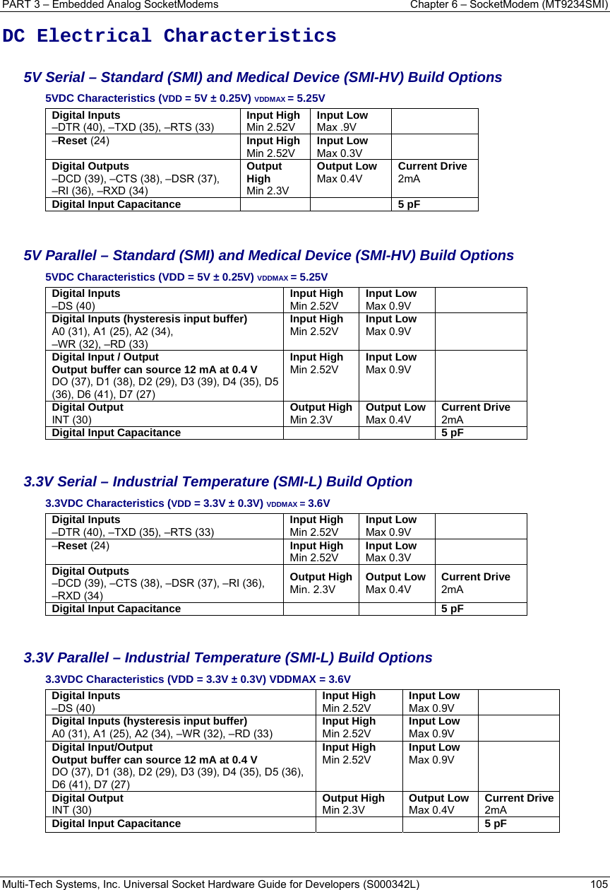
![PART 3 – Embedded Analog SocketModems Chapter 6 – SocketModem (MT9234SMI) Multi-Tech Systems, Inc. Universal Socket Hardware Guide for Developers (S000342L) 101 Technical Specifications The SocketModem (MT9234SMI) meets the following specifications: Category Description Data Standards V.92, V.34 enhanced, V.34, V.32bis, V.32, V.22bis, V.22; Bell 212A and Bell 103 Data Format Serial, or 8-bit parallel interface, asynchronous Character Format 10 bit or 11 bit Serial/Data Speeds Serial port data rates adjustable to 300, 1200, 2400, 4800, 9600, 19200, 38400, 57600, 115200, and 230400 bps Client-to-Client Data Rates 33600, 31200, 28800, 26400, 24000, 21600, 19200, 16800, 14400, 12000, 9600, 7200, 4800, 2400, 1200, 0-300 bps Data Error Correction (ECM) V.44; V.42 (LAPM, MNP 2-4) Data Compression V.42bis, MNP 5 Fax Compatibility V.17, V.29/V.27/V.21, V.34 Fax Class Class 1 &1.0 – All builds Class 2, 2.0/2.1 – All builds Fax Compression MH, MR, MMR Fax Error Correction Mode ECM Modes of Operation Fax online modes; full duplex over dial-up lines; data mode; command mode; online command mode; V.54 test mode Weight 0.6 oz. (0.017 kg.) Operating Temperature -40° to +85° C Storage Temperature -40° to +85° C Humidity 20% to 90% (non-condensing) Operating Voltage 3.3V and 5V Power Measurements MT9234SMI 3.3V Typical: 122mA (0.40W @ 3.3VDC) Maximum: 136mA (0.49W @ 3.6VDC) Sleep Mode: 90mA to 95mA (.297W to .3135W @ 3.3VDC) 5V Typical: 125mA (0.62W @ 5VDC) Maximum: 138mA (0.72W @ 5.25VDC) Sleep Mode: 92mA (0.44W @ 5VDC) Note: Multi-Tech Systems, Inc. recommends that the customer incorporate a 10% buffer into their power source when determining product load. Transmit Level - 11 dBm (varies by country setting) Receiver Sensitivity - 43 dBm under worst-case conditions DAA Isolation MT9234SMI 1.5Kv r.m.s. or 2121 VDC at working voltage of 250VAC MT9234SMI 2Kv r.m.s. or 2828VDC at working voltage of 125VAC Flow Control XON/XOFF (software), RTS/CTS (hardware) Command Buffer 60 characters Telephony / TAM TAM: S-101 AT+V commands (no CODEC for speakers/microphone interface) Certifications & Approvals Safety Certifications UL 60950 cUL 60950 EN 60950 AS/NZS 60950:2000 CCC Safety Certifications for HV Builds UL 60601-1 EN 60601-1 EMC Approvals FCC Part 15 Canadian EMC EN 55022 EN 55024 GB4943, GB9254 Warranty 2 years Comment [DAR49]: This came from email string involving Curt, Brandon Dalida, Jerome, dated 2/5/09 forwarded by Jerry to me. It covers sleep mode for the 5634SMI-ITP too.](https://usermanual.wiki/Multi-Tech-Systems/92U09G17825.User-Manual/User-Guide-1204041-Page-101.png)
![PART 3 – Embedded Analog SocketModems Chapter 6 – SocketModem (MT9234SMI) Multi-Tech Systems, Inc. Universal Socket Hardware Guide for Developers (S000342L) 103 SocketModem Pin Out Serial Pin Out The MT9234SMI SocketModem uses a 20-pin interface to provide an on-board DAA with tip and ring connections, audio circuit for call-progress monitoring, LED driver for call status annunciation, and serial interface. Note: The bolded, shaded pins are the active MT9234SMI pins. Top View Serial SocketModem Pin Out For pin descriptions, see the Universal Pin Out Descriptions in Chapter 1. Comment [DAR50]: Pinout 9234.png filed under rev K graphics](https://usermanual.wiki/Multi-Tech-Systems/92U09G17825.User-Manual/User-Guide-1204041-Page-103.png)
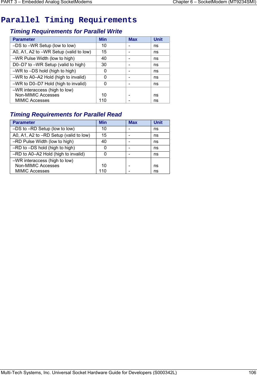
![PART 3 – Embedded Analog SocketModems Chapter 6 – SocketModem (MT9234SMI) Multi-Tech Systems, Inc. Universal Socket Hardware Guide for Developers (S000342L) 104 Parallel Pin Out The parallel configuration is not compatible with the serial universal socket. The Parallel SocketModem uses a 22-pin interface to provide an on-board DAA with tip and ring connections, audio circuit for call-progress monitoring, and parallel interface. Note: The bolded, shaded pins are the active MT9234SMI-P (Parallel) pins. Top View – Parallel SocketModem Pins Pin Descriptions for a Parallel SocketModem Device Pin # Signal I/O Description 1 Tip I/O Telephone Line Interface – TIP 2 Ring I/O Telephone Line Interface – RING 24 –RESET I Modem Reset (with pull-up). Active low –RESET input resets the SocketModem logic and returns AT command set to original factory defaults or to NVRAM 'stored values' . The modem is ready to accept commands within 6.5 seconds of power-on or reset. Reset must be asserted for a minimum of 30ms. 25 A1 I Host Bus Address Line 1 26 DGND GND Digital Ground 27 D7 O Host Bus Data Line 7 29 D2 O Host Bus Data Line 2 30 INT O Host Bus Interrupt Line. INT output is set high when the receiver error flag, receiver data available, transmitter holding register empty, or modem status interrupt have an active high condition. INT is reset low upon the appropriate interrupt service or master reset operation. 31 A0 I Host Bus Address Line 0. 32 –WR I Host Bus Write. –WR is an active low, write control input. When –DS is low, –WR low allows the host to write data or control words into a selected modem register. 33 –RD I Host Bus Read. –RD is an active low, read control input. When –DS is low, –RD low allows the host to read status information or data from a selected modem register. 34 A2 I Host Bus Address Line 2 35 D4 O Host Bus Data Line 4 36 D5 O Host Bus Data Line 5 37 D0 O Host Bus Data Line 0 38 D1 O Host Bus Data Line 1 39 D3 O Host Bus Data Line 3 40 –DS I Host Bus Device Select. –DS input low enables the modem for read or write. 41 D6 O Host Bus Data Line 6 61 VCC PWR +5 V or 3.3 V Supply (depends upon model). 63 AGND GND Analog Ground. This is tied common with DGND on the SocketModem. To minimize potential ground noise issues, connect audio circuit return to AGND. 64 SPKR O Speaker Output. SPKR is a single ended-output. It is tied to the CODEC through a series 6.8K resistor and .1uf cap. Comment [DAR51]: SM Analog Dial-up Parallel.wmf](https://usermanual.wiki/Multi-Tech-Systems/92U09G17825.User-Manual/User-Guide-1204041-Page-104.png)
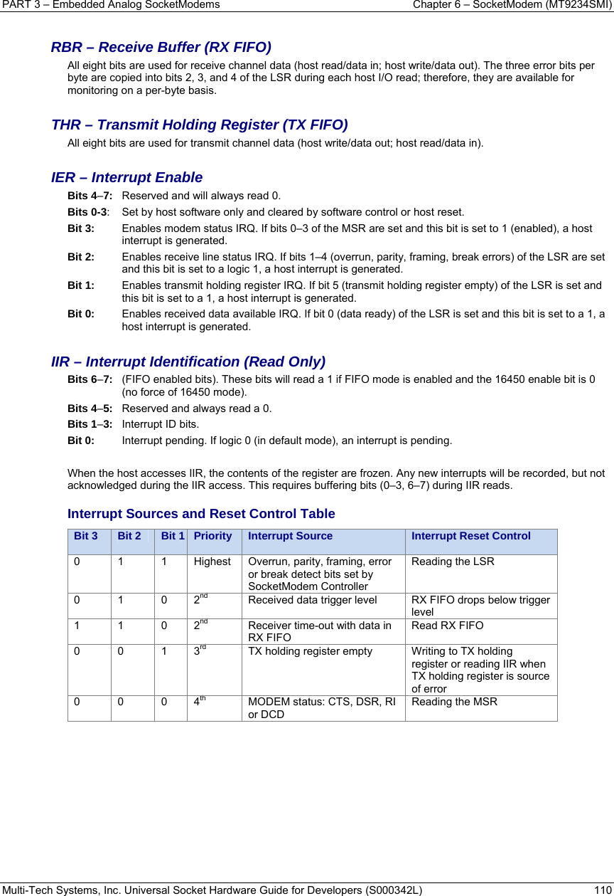
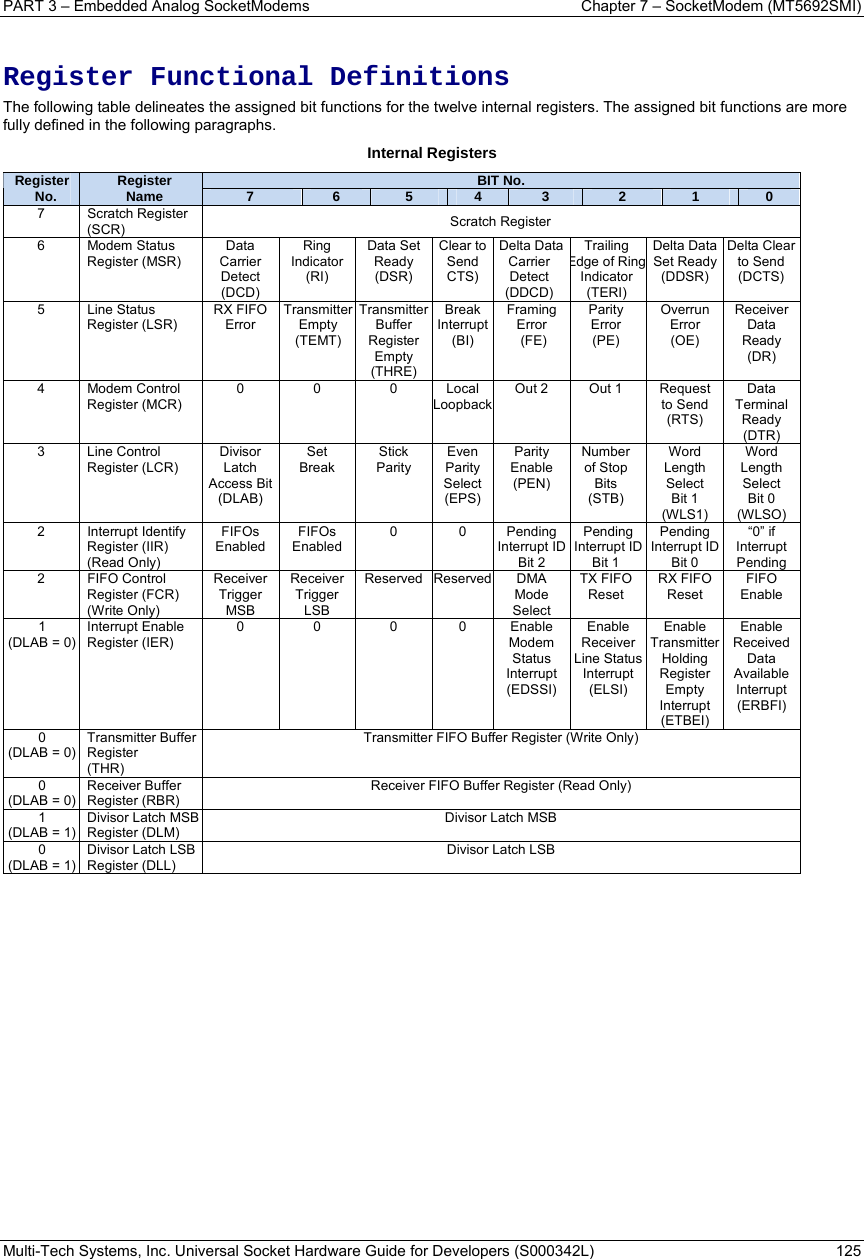
![PART 3 – Embedded Analog SocketModems Chapter 6 – SocketModem (MT9234SMI) Multi-Tech Systems, Inc. Universal Socket Hardware Guide for Developers (S000342L) 109 Register Functional Definitions The following table delineates the assigned bit functions for the twelve internal registers. The assigned bit functions are more fully defined in the following paragraphs. Internal Registers A2 A1 A0 Register [Default] *3 BIT-7 BIT-6 BIT-5 BIT-4 BIT-3 BIT-2 BIT-1 BIT-0 General Register Set: Note 1* 0 0 0 RBR [XX] Bit-7 Bit-6 Bit-5 Bit-4 Bit-3 Bit-2 Bit-1 Bit-0 0 0 0 THR [XX] Bit-7 Bit-6 Bit-5 Bit-4 Bit-3 Bit-2 Bit-1 Bit-0 0 0 1 IER [00] 0 0 0 0 Modem Status Interrupt Receive Line Status interrupt Transmit Holding Register interrupt Receive Holding Register interrupt 0 1 0 IIR [XX] FIFO enable FIFO enable 0 0 Interrupt ID Interrupt ID Interrupt ID Interrupt Pending 0 1 0 FCR [00] RX Trigger (MSB) RX trigger (LSB) Detect change in FCR TX FIFO overrun bit DMA mode select XMIT FIFO reset RCVR FIFO resetFIFO enable 0 1 1 LCR [00] Divisor latch access (DLAB) Set break Stick parity Even parity Parity enable 0 Word length bit-1 Word length bit-0 1 0 0 MCR [00] 0 0 0 Loop back INT enable OUT 1 -RTS -DTR 1 0 1 LSR [60] RX FIFO data error TX empty THR empty THR Empty Break interrupt Framing error Parity error Overrun error Receive data ready 1 1 0 MSR [X0] CD RI DSR CTS Delta -CD Delta -RI Delta -DSR Delta -CTS 1 1 1 SCR [FF] Bit-7 Bit-6 Bit-5 Bit-4 Bit-3 Bit-2 Bit-1 Bit-0 Special Register Set: Note *2 0 0 0 DLL [00] Bit-7 Bit-6 Bit-5 Bit-4 Bit-3 Bit-2 Bit-1 Bit-0 0 0 1 DLM [00] Bit-7 Bit-6 Bit-5 Bit-4 Bit-3 Bit-2 Bit-1 Bit-0 Note: 1* The General Register set is accessible only when DS is a logic 0. 2* The Baud Rate register set is accessible only when DS is a logic 0 and LCR bit-7 is a logic 1. 3* The value between the square brackets represents the register's initialized HEX value, X = N/A.](https://usermanual.wiki/Multi-Tech-Systems/92U09G17825.User-Manual/User-Guide-1204041-Page-109.png)
![PART 3 – Embedded Analog SocketModems Chapter 6 – SocketModem (MT9234SMI) Multi-Tech Systems, Inc. Universal Socket Hardware Guide for Developers (S000342L) 114 Application Notes Tip and Ring Interface OEM Motherboard Filtering and Surge Protection Options See Design Considerations and Recommended Parts in Chapter 1. Recommended Uses for Filtering Options Enhanced Surge Protection with RJ-11 Filtering Use this option when additional lightning protection may be needed. Alternate Common Mode with RJ-11 Filtering Use this option when your design has common mode emission issues. Comment [DAR52]: This is the new Tip and Ring done 2008 Comment [DAR53]: Tip_and_Ring_New_2008.png Rev. I](https://usermanual.wiki/Multi-Tech-Systems/92U09G17825.User-Manual/User-Guide-1204041-Page-114.png)
![PART 3 – Embedded Analog SocketModems Chapter 7 – SocketModem (MT5692SMI) Multi-Tech Systems, Inc. Universal Socket Hardware Guide for Developers (S000342L) 117 Technical Specifications MT5692SMI, MT5692SMI-V, MT5692SMI-P, MT5692SMI-IP The MT5692SMI, MT5692SMI-V, MT5692SMI-P, and MT5692SMI-IP SocketModems meet the following specifications: Category Description Data Standards V.92, V.34, V.32bis, V.32, V.23, V.23 half-duplex, V.23 reverse, V.22bis, V.22bis Fast Connect, V.22, V.21, Bell 212A/Bell 103, V.29 FastPOS, V.80 Synchronous Access Mode (V.80 not for IP build) Data Format All Builds: Serial, asynchronous Parallel Build: 8-bit parallel interface Character Format 10 bit Serial/Data Speeds All Builds Except IP: Supports DTE speeds up to 230.4K bps, autobaud up to 115.2K bps For IP Build: Supports DTE speeds up to 921.6K bps, Client-to-Client Data Rates 33600, 31200, 28800, 26400, 24000, 21600, 19200, 16800, 14400, 12000, 9600, 7200, 4800, 2400, 1200, 0-300 bps Data Error Correction V.42 LAPM and MNP 2–4 Data Compression V.44, V.42bis, MNP 5 Fax Compatibility All Builds Except IP: V.17, V.29, V.27ter, V.21 channel 2 Fax Class All Builds Except IP: Class 1, Class 1.0 Modes of Operation Full duplex over dial-up lines; data mode, command mode, online command mode Size 2.54" (64.541 mm) x 1.045" (26.543 mm) Weight 0.6 oz. (0.017 kg.) Operating Temperature -40º to +85° C Storage Temperature -40º to +85° C Humidity 20% to 90% (non-condensing) Operating Voltage 3.3V or 5V Note: Voice modules are available with 5V only Transmit Level -12 dBm (varies by country) Receiver Sensitivity -43 dBm under worst-case conditions DAA Isolation 1.5Kv r.m.s. or 2121 VDC at working voltage of 250VAC Flow Control All Builds Except IP: XON/XOFF (software), RTS/CTS (hardware) Command Buffer 60 characters Telephony/TAM V.253 commands 8 kHz sample rate Concurrent DTMF, distinctive ring, and "Bell Core Type 1" Caller ID 8-bit μ-law and A-law PCM coding Supports PCM Encoding: 2-bit and 4-bit ADPCM, 8-bit and 16-bit linear PCM, and 4-bit IMA coding Compliance EMC Compliance FCC Part 15 (Class B) ICES-003 (Class B) EN 55022 (Class B) EN 55024 Safety Compliance UL 60950-1 cUL 60950-1 EN 60950-1 AS/NZS 60950:2000 Telecom 47 CFR Part 68 CS-03 R&TTE A-Tick (Other countries included per the Modem Globalization Guide) Warranty 2 years Comment [DAR54]: 115.2K bps came from Mike L. 7/14/09 Comment [DAR55]: 921.6K bps came from Mike L. 7/14/09](https://usermanual.wiki/Multi-Tech-Systems/92U09G17825.User-Manual/User-Guide-1204041-Page-117.png)
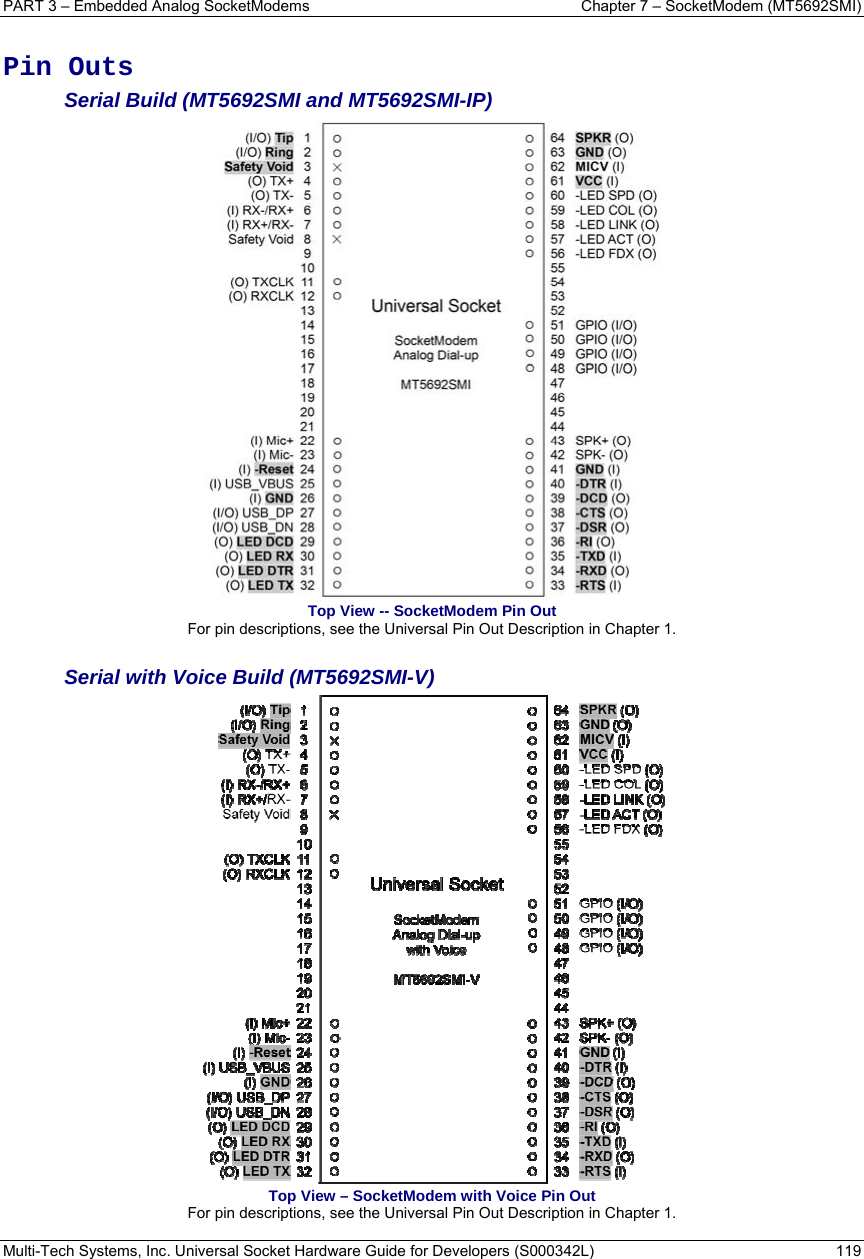
![PART 3 – Embedded Analog SocketModems Chapter 7 – SocketModem (MT5692SMI) Multi-Tech Systems, Inc. Universal Socket Hardware Guide for Developers (S000342L) 120 Parallel Build (MT5692SMI-P) Top View – SocketModem with Parallel Build Pin Out For pin descriptions, see the Universal Pin Out Description in Chapter 1. Parallel Pin Descriptions Pin # Signal Name In Out Type Description 1 Tip I/O Telephone Line Interface – TIP 2 Ring I/O Telephone Line Interface – RING 24 –RESET I Modem Reset (CMOS input with pull-up). The active low –RESET input resets the SocketModem logic and returns the AT command set to the original factory default values or to "stored values" in NVRAM. The modem is ready to accept commands within 6.5 seconds of power-on or reset. 25 A1 I Host Bus Address Line 1 26 DGND GND Digital Ground 27 D7 O Host Bus Data Line 7 29 D2 O Host Bus Data Line 2 30 INT O Host Bus Interrupt Line (Active High, Resets on Low) 31 A0 I Host Bus Address Line 0 32 –WR I Host Bus Write. When low, allows host to write to SocketModem. 33 –RD I Host Bus Read. When low, allows host to read from SocketModem. 34 A2 I Host Bus Address Line 2 35 D4 O Host Bus Data Line 4 36 D5 O Host Bus Data Line 5 37 D0 O Host Bus Data Line 0 38 D1 O Host Bus Data Line 1 39 D3 O Host Bus Data Line 3 Comment [DAR56]: This sentence removed from reset by Dustin 8/24/09 Reset must be asserted for a minimum of 15ms.](https://usermanual.wiki/Multi-Tech-Systems/92U09G17825.User-Manual/User-Guide-1204041-Page-120.png)
![PART 3 – Embedded Analog SocketModems Chapter 7 – SocketModem (MT5692SMI) Multi-Tech Systems, Inc. Universal Socket Hardware Guide for Developers (S000342L) 122 Power* Measurements Serial Build – MT5692SMI Serial with IP Build – MT5692SMI-IP Input Voltage: 3.3V Sleep Mode Typical Maximum Current (AMPS) 0.047 0.101 0.112 Watts 0.151 0.316 0.349 Input Voltage: 5V Sleep Mode Typical Maximum Current (AMPS) 0.052 0.109 0.121 Watts 0.256 0.528 0.583 Voice Build – MT5692SMI-V Note: The voice build is not available in 3.3V. Input Voltage: 5V Sleep Mode Typical Maximum Current (AMPS) 0.016 0.076 0.089 Watts 0.080 0.380 0.445 Parallel Build – MT5692SMI-P Input Voltage: 3.3V Sleep Mode Typical Maximum Measured Voltage 3.30 3.29 3.29 Current (AMPS) 0.015 0.072 0.081 Watts 0.051 0.236 0.267 Input Voltage: 5V Sleep Mode Typical Maximum Measured Voltage 4.91 4.86 4.84 Current (AMPS) with 5V 0.014 0.069 0.079 Watts 0.068 0.334 0.380 Note: Multi-Tech Systems, Inc. recommends that the customer incorporate a 10% buffer into their power source when determining product load. Input Voltage: 3.3V Sleep Mode Typical Maximum Current (AMPS) 0.014 0.069 0.080 Watts 0.046 0.216 0.249 Input Voltage: 5V Sleep Mode Typical Maximum Current (AMPS) 0.018 0.074 0.088 Watts 0.089 0.359 0.425 Comment [DAR57]: This were updated on 10/16/09 with new info from Tom Fix.](https://usermanual.wiki/Multi-Tech-Systems/92U09G17825.User-Manual/User-Guide-1204041-Page-122.png)
![PART 3 – Embedded Analog SocketModems Chapter 7 – SocketModem (MT5692SMI) Multi-Tech Systems, Inc. Universal Socket Hardware Guide for Developers (S000342L) 123 Parallel Host Bus Timing Table Symbol Parameter Min Max Units READ (See Notes) tAS Address Setup 5 - ns tAH Address Hold 5 - ns tCS Chip Select Setup 5 - ns tCH Chip Select Hold 0 - ns tRD RD Strobe Width 77 - ns tDD Read Data Delay 10 25 ns tDRH Read Data Hold 5 - ns WRITE (See Notes) tAS Address Setup 5 - ns tAH Address Hold 5 - ns tCS Chip Select Setup 0 - ns tCH Chip Select Hold 10 - ns tWT WT Strobe Width 15 - ns tDS Write Data Setup (see Note 4) 15 20 ns tDWH Write Data Hold (see Note 5) 5 - ns Notes: 1. When the host executes consecutive Rx FIFO reads, a minimum delay of 2 times the internal CPU clock cycle plus 15 ns (85.86 ns at 28.224 MHz) is required from the falling edge of RD to the falling edge of the next Host Rx FIFO RD clock. 2. When the host executes consecutive Tx FIFO writes, a minimum delay of 2 times the internal CPU clock cycle plus 15 ns (85.86 ns at 28.224 MHz) is required from the falling edge of WT to the falling edge of the next Host Tx FIFO WT clock. 3. tRD' tWT = tCYC + 15 ns. 4. tDS is measured from the point at which both CS and WT are active. 5. tDWH is measured from the point at which either CS and WT become active. 6. Clock Frequency = 1.8432 MHz clock. Parallel Host Bus – Read Parallel Host Bus - Write Comment [DAR58]: Changed by Mike McNeil 7/9/09- Parallel Host Bus Timing Table - For READ change, Address Hold to 5, Chip Select Setup to 5, Chip Select Hold to 0, RD Strobe Width to 77, Read Data Delay to 10. For WRITE change, Address Hold to 5, WT Strobe Width to 15, Write Data Setup to 15. - 6. Clock Frequency is 1.8432MHz. Comment [DAR59]: Parallel_Host_Bus_Read.bmp 31KB Comment [DAR60]: Parallel_host_Bus_Write.bmp 31Kb](https://usermanual.wiki/Multi-Tech-Systems/92U09G17825.User-Manual/User-Guide-1204041-Page-123.png)
![PART 3 – Embedded Analog SocketModems Chapter 7 – SocketModem (MT5692SMI) Multi-Tech Systems, Inc. Universal Socket Hardware Guide for Developers (S000342L) 131 LSR – Line Status Register (Addr = 5) This 8-bit register provides status information to the host concerning data transfer Bit 7 RX FIFO Error In the 16450 mode, this bit is not used and is always 0. In the FIFO mode, this bit is set if there are one or more characters in the RX FIFO with parity error, framing error, or break indication detected. This bit is reset to a 0 when the host reads the LSR and note of the above conditions exist in the RX FIFO. Bit 6 Transmitter Empty (TEMT) This bit is set to a 1 whenever the TX Buffer (THR) and equivalent of the Transmitter Shift Register (TRS) are both empty. It is reset to a 0 whenever either the THR or the equivalent of the TSR contains a character. In the FIFO mode, this bit is set to a 1 whenever the TX FIFO and the equivalent of the TSR are both empty Bit 5 Transmitter Holding Register Empty (THRE) [TX Buffer Empty] This bit, when set, indicates that the TX Buffer is empty and the modem can accept a new character for transmission. In addition, this bit causes the modem to issue an interrupt to the host when the Transmit Holding Register Empty Interrupt Enable bit (IIR1) is set to 1. The THRE bit is set to a 1 when a character is transferred from the TX Buffer. The bit is reset to 0 when a byte is written into the TX Buffer by the host. In the FIFO mode, this bit is set when the TX FIFO is empty; it is cleared when at least one byte is in the TX FIFO. Bit 4 Break Interrupt (BI) This bit is set to a 1 whenever the received data input is a space (logic 0) for longer than two full word lengths plus 3 bits. The BI is reset when the host reads the LSR. Bit 3 Framing Error (FE) This bit indicates that the received character did not have a valid stop bit. The FE bit is set to a 1 whenever the stop bit following the last data bit or parity bit is detected as a logic o (space). The FE bit is reset to a 0 when the host reads the LSR. In the FIFO mode, the error indication is associated with the particular character in the FIFO it applies to. The FE bit set to a 1 when this character is loaded into the RX Buffer. Bit 2 Parity Error (PE) This bit indicates that the received data character in the RX Buffer does not have the correct even or odd parity, as selected by the Even Parity Select bit (LCR4) and the Stick Parity bit (LCR5). The PE bit is reset to a 0 when the host reads the LSR. In the FIFO mode, the error indication is associated with the particular character in the FIFO it applies to. The PE bit set to a 1 when this character is loaded into the RX Buffer. Bit 1 Overrun Error (OE) This bit is set to a 1 whenever received data is loaded into the RX Buffer before the host has read the previous data from the RX Buffer. The OE is reset to a 0 when the host reads the LSR. In the FIFO mode, if data continues to fill beyond the trigger level, an overrun condition will occur only if the RX FIFO is full and the next character has been completely received. Bit 0 Receiver Data Ready (DR) This bit is set to a 1 whenever a complete incoming character has been received and transferred into the RX Buffer. The DR bit is reset to a 0 when the host reads the RX Buffer. In the FIFO mode, the DR bit is set when the number of received data bytes in the RX FIFO equals or exceeds the trigger level specified in the FCR0-FCR1.](https://usermanual.wiki/Multi-Tech-Systems/92U09G17825.User-Manual/User-Guide-1204041-Page-131.png)
![PART 3 – Embedded Analog SocketModems Chapter 7 – SocketModem (MT5692SMI) Multi-Tech Systems, Inc. Universal Socket Hardware Guide for Developers (S000342L) 134 Application Notes Tip and Ring Interface OEM Motherboard Filtering and Surge Protection Options See Design Considerations and Recommended Parts in Chapter 1. Recommended Uses for Filtering Options Enhanced Surge Protection with RJ-11 Filtering Use this option when additional lightning protection may be needed. Alternate Common Mode with RJ-11 Filtering Use this option when your design has common mode emission issues. Comment [DAR61]: Tip_and_Ring_New_2008.png](https://usermanual.wiki/Multi-Tech-Systems/92U09G17825.User-Manual/User-Guide-1204041-Page-134.png)
![PART 3 – Embedded Analog SocketModems Chapter 7 – SocketModem (MT5692SMI) Multi-Tech Systems, Inc. Universal Socket Hardware Guide for Developers (S000342L) 135 Microphone and Speaker Note: Applies to the MT5692SMI Voice only. Microphone Input Option Speaker Output Option 1 Speaker Output Option 2 Differences between Speaker 1 Example and Speaker 2 Example Speaker 1 does not have an amplifier while Speaker 2 does. Comment [DAR62]: Filtering-mic-option.png filed under Universal_SocketModem\Graphics\Mike_Z_Filtering_Drawings Comment [DAR63]: Filtering-Speaker1.png filed under Universal_SocketModem\Graphics\Mike_Z_Filtering_Drawings Comment [DAR64]: Filtering-Speaker1.png filed under Universal_SocketModem\Graphics\Mike_Z_Filtering_Drawings](https://usermanual.wiki/Multi-Tech-Systems/92U09G17825.User-Manual/User-Guide-1204041-Page-135.png)
![PART 3 – Embedded Analog SocketModems Chapter 7 – SocketModem (MT5692SMI) Multi-Tech Systems, Inc. Universal Socket Hardware Guide for Developers (S000342L) 136 Specifications for the Microphone Input Impedance >70K ohms AC Input Voltage Range 1.1V P-P Reference Voltage 1.35V Specifications for the Speaker Output from the Codec Minimum Load 300 Maximum Capacitive Load 0.01 uF Output Impedance 10 AC Output Voltage Range 1.4V P-P Reference voltage +1.35 VDC DC Offset Voltage 20 mV Speaker Output The speaker output from the codec is coupled to the speaker pin (64) through a 1uF cap and a 33 ohm resistor. The speaker pin is shared with the call progress monitor which is a digital I/O pin on the DSP that is coupled to the speaker pin through a 1uF and 3.9K. Comment [DAR65]: This text came from the Conexant Codec data sheet, document CX20437, page 44.](https://usermanual.wiki/Multi-Tech-Systems/92U09G17825.User-Manual/User-Guide-1204041-Page-136.png)
![Chapter 8 – SocketModem (MT2492SMI) Multi-Tech Systems, Inc. Universal Socket Hardware Guide for Developers (S000342L) 139 SocketModem Pin Out The MT2492SMI SocketModem with a serial interface provides an on-board DAA with tip and ring connections, audio circuit for call-progress monitoring and serial interface via logic level signals. Note: The bolded, shaded pins are active MT2492MI pins. Top View Serial SocketModem Pin Out For pin descriptions, see the Universal Pin Out Description in Chapter 1. DC Electrical Characteristics 3.3V Serial SocketModem 3.3VDC Characteristics (VDD = 3.3V ± 0.3V) VDDMAX = 3.6V Inputs Input High Input Low –DTR (40), –TXD (35), –RTS (33), –RESET (24) Min 2.0V Max 0.8V Outputs Output High Output Low –DCD (39), –CTS (38), –DSR (37), –RI (36), –RXD (34) 2mA, Z INT = 120 Ω Min 2.4V Max 0.4V Digital Input Capacitance 50pF 5V Serial SocketModem 5VDC Characteristics (VDD = 5V ± 0.25V) VDDMAX = 5.25V Inputs Input High Input Low –DTR (40), –TXD (35), –RTS (33), –RESET (24) Min 2.0V Max 0.8V Outputs Output High Output Low –DCD (39), –CTS (38), –DSR (37), –RI (36), –RXD (34) 2mA, Z INT = 120 Ω Min 2.4V Max 0.4V Digital Input Capacitance 50pF Comment [DAR66]: Pin Out_MT2492SMI.FH9 & .png](https://usermanual.wiki/Multi-Tech-Systems/92U09G17825.User-Manual/User-Guide-1204041-Page-139.png)
![Chapter 8 – SocketModem (MT2492SMI) Multi-Tech Systems, Inc. Universal Socket Hardware Guide for Developers (S000342L) 140 Application Notes Tip and Ring Interface OEM Motherboard Filtering and Surge Protection Options See Design Considerations and Recommended Parts in Chapter 1. Recommended Uses for Filtering Options Enhanced Surge Protection with RJ-11 Filtering Use this option when additional lightning protection may be needed. Alternate Common Mode with RJ-11 Filtering Use this option when your design has common mode emission issues. Comment [DAR67]: New Tip and Ring 2008 Comment [DAR68]: Filtering_MT2492SMI_RJ11-Filtering_b_MikeZ.bmp Comment [DAR69]: Tip_and_Ring_3rd_section.png Stored under CurrentProj_Universal Guide (for Rev-G. Copied from Tip_and_Ring_New_fromMikeZ_Schematic1_Page1_border_removed.FH9 Will be moved with Rev G material. Comment [DAR70]: Tip_and_Ring_New_2008.png Rev. I](https://usermanual.wiki/Multi-Tech-Systems/92U09G17825.User-Manual/User-Guide-1204041-Page-140.png)
![PART 3 – Embedded Analog SocketModems Chapter 9 – SocketModem (MT2456SMI-22) Multi-Tech Systems, Inc. Universal Socket Hardware Guide for Developers (S000342L) 143 SocketModem Configuration Serial Configuration The MT2456SMI-22 SocketModem with a serial interface uses a 20-pin interface to provide an on-board DAA with tip and ring connections, audio circuit for call-progress monitoring and serial interface via logic level signals. Note: The bolded, shaded pins are active MT2456SMI-22 pins. Top View Serial SocketModem Pinout For pin descriptions, see the Universal Pinout Descriptions in Chapter 1. Comment [DAR71]: 2456SMI.png](https://usermanual.wiki/Multi-Tech-Systems/92U09G17825.User-Manual/User-Guide-1204041-Page-143.png)
![PART 3 – Embedded Analog SocketModems Chapter 9 – SocketModem (MT2456SMI-22) Multi-Tech Systems, Inc. Universal Socket Hardware Guide for Developers (S000342L) 145 Applications Notes Tip and Ring Interface OEM Motherboard Filtering and Surge Protection Options See Design Considerations and Recommended Parts in Chapter 1. Comment [DAR72]: Tip_and_Ring_New_2008.png Rev. I](https://usermanual.wiki/Multi-Tech-Systems/92U09G17825.User-Manual/User-Guide-1204041-Page-145.png)
![PART 4 – Embedded Device Servers Chapter 10 – SocketEthernet IP (MT100SEM-IP) Multi-Tech Systems, Inc. Universal Socket Hardware Guide for Developers (S000342L) 148 Technical Specifications The SocketEthernet IP (MT100SEM-IP) meets the following specifications: Category Description Interfaces 10/100BaseT Ethernet, Asynchronous Serial Serial Character Format 8N1 (Data, Parity, and Stop bits are configurable) Serial/Data Speeds 300 to 921600 bps Ethernet Data Speeds 10MB or 100MB Physical Description 2.541" L × 1.045" W × 0.680" H; 0.6 oz. (6.45 cm × 2.65 cm × 1.7 cm; 0.017 kg.) Operating Temperature 0 to +70 C Storage Temperature -40 C to +85 C Humidity 20% to 90% (non-condensing) Operating Voltage 5VDC or 3.3VDC Power Measurements See the Power Measurements table. Flow Control RTS/CTS (hardware) Network Protocols Supported ARP, DHCP client, DNS client, FTP, ICMP (ping), IP, POP3, SMTP, TCP, Telnet server, UDP Management Serial Telnet Web-based configuration Certifications & Approvals Safety Certifications UL 60950 cUL 60950 EN 60950 AS/NZS 60950:2000 Safety Certifications for High Voltage Build UL 60601-1 EN 60601-1 EMC Approvals FCC Part 15 Class B Canada Class B EN 55022 Class B EN 55024 Warranty 2 years Intelligent Features Complete serial-to-Ethernet connectivity solution including network processor, media access controller and physical interface. AT Command compatible LED driver outputs for visual monitoring speed, link, activity, collision and duplex mode Half duplex or full duplex support on the LAN interface Central site setup and control of the remote communications device. Flash memory to update firmware with the latest enhancements Comment [DAR73]: From Dustin 6/24/09](https://usermanual.wiki/Multi-Tech-Systems/92U09G17825.User-Manual/User-Guide-1204041-Page-148.png)
![PART 4 – Embedded Device Servers Chapter 10 – SocketEthernet IP (MT100SEM-IP) Multi-Tech Systems, Inc. Universal Socket Hardware Guide for Developers (S000342L) 149 SocketEthernet IP Pin Out The SocketEthernet IP uses a 22-pin interface to provide an on-board Ethernet media access controller, an Ethernet physical layer (without the RJ-45 jack), an LED driver for Ethernet monitoring, and a serial interface. Note: The shaded, bolded pins are SocketEthernet IP active pins. Top View SocketEthernet IP MT100SEM-IP Pin Out For pin descriptions, see the Universal Pin Out Descriptions in Chapter 1.Comment [DAR74]: M100SEM.png](https://usermanual.wiki/Multi-Tech-Systems/92U09G17825.User-Manual/User-Guide-1204041-Page-149.png)
![PART 4 – Embedded Device Servers Chapter 10 – SocketEthernet IP (MT100SEM-IP) Multi-Tech Systems, Inc. Universal Socket Hardware Guide for Developers (S000342L) 151 Application Notes Ethernet Interface – Non-Isolated Design Note: VREF stands for Power in this drawing. Ethernet Interface – Isolated Design Isolated Design Application Note The MT100SEM-L-HV-IP was designed to meet Basic Isolation at 240Vac according to the international medical directive for safety (EN60601-1). The recommended components for an isolated design comply with the same standard. Recommended Parts Recommended Capacitors for a Non-Isolated Design: Manufacturer – NIC Components Corp. Part Number – NMC0603NPO150J50TRPF Recommended Safety Rated Capacitors for an Isolated Design: The recommended capacitors are Y2 rated and meet supplementary isolation at 240Vac along with the required creepages and clearances. Manufacture – NOVACAP Part Number – ES2211N(value)K502NXT Recommended Resistor: The resistors are 75 ohms 1/8 watt. Recommended Ethernet Modular Jack: The recommended jack is an eight contact, eight position, unshielded and ungrounded connector that will maintain the need isolation and spacing requirements. A shielded and grounded connector may be used, but special consideration must be made for the isolation and spacing requirements. Manufacture – Stewart Connector Systems Part Number – SS-6488-NF-K1 Comment [DAR75]: MT100SEM IP Non Isolated Scan0578_000.jgp 97KB jpg was smaller than png. Filed under CurrentProj_Universal_Guide_2009_Rev_J\Graphics Comment [DAR76]: MT100SEM IP Isolated Scan0579_000.jpg (jpg was smaller than png) 169KB. Filed under CurrentProj_Universal_Guide_2009_Rev_J\Graphics](https://usermanual.wiki/Multi-Tech-Systems/92U09G17825.User-Manual/User-Guide-1204041-Page-151.png)

![PART 4 – Embedded Device Servers Chapter 10 – SocketEthernet IP (MT100SEM-IP) Multi-Tech Systems, Inc. Universal Socket Hardware Guide for Developers (S000342L) 153 The Windows-Based Auto-Discovery Manager The Auto-Discovery Manager is a mechanism for remotely monitoring the Universal IP functioning. It also provides support for configuring several key parameters, such as DHCP Status (enable/disable), IP Address, and the Host Name of an MT100SEM-IP. The Auto-Discovery mechanism is utilized by running a Windows-based Server Application that can monitor/configure the MT100SEM-IP. Communication between the MT100SEM-IP and the Windows-based Server is through MAC level broadcasts on a configured UDP port. Two Ways to Use Auto Discovery: Auto-Discovery can be performed by using AT Commands (see the Universal IP AT Commands Reference Guide – included on the Universal Kit CD) or by using the Auto-Discover Manager Software (also included on the Universal Kit CD). Auto-Discovery Manager Software The Auto-Discovery Manager is composed of two components: The Client Component – The Client component periodically broadcasts its current configuration over the network. The Server Component – The Server component receives the broadcasts from the client. Client Component The Auto-Discovery Client component is integrated with MT100SEM-IP. It broadcasts its current configuration over the network on a specific UDP SERVER-PORT. By default the SERVER-PORT is set to 1020. The configuration parameters broadcast are Version details MAC Address Static IP Address DHCP Status DHCP Assigned IP Address Host Name Broadcast interval Port number on which the client listens Server Component The Server component listens on the SERVER-PORT. It receives the broadcasts from the client and updates the list of configuration parameters. This list can be viewed by the administrator through the User Interface: The List of Entries Detailed Information about a Selected Entry Log Files will display here Comment [DAR77]: Auto Discovery Screen1.jpg (jpg was smaller than png) 184KB. CurrentProj_Universal_Guide_2009_Rev_J\Graphics\Auto Discovery for Universal](https://usermanual.wiki/Multi-Tech-Systems/92U09G17825.User-Manual/User-Guide-1204041-Page-153.png)
![PART 4 – Embedded Device Servers Chapter 10 – SocketEthernet IP (MT100SEM-IP) Multi-Tech Systems, Inc. Universal Socket Hardware Guide for Developers (S000342L) 154 How to View the Detailed Information New entries are appended to the list shown on the screen above. Only the first ten entries are displayed on the screen. However the administrator can scroll down to view more entries. Clicking on an entry displays the detailed information about that entry. How to Edit the List and Make the Changes Permanent 1. Double-click on the entry you wish to edit. 2. After clicking the desired entry, a new dialog box displays showing the current configuration. 3. Enter the new parameters and click the SET button. The server sends the modified parameters to the client. Upon receiving the broadcast from the Server, the Client validates the packet. The Client determines whether the packet is destined for its own MAC Address. If so, it sets the modified parameters that are different from its current configuration, and the it broadcast the newly configured parameters. The Client Status is set to Active upon the receipt of a broadcast packet. The Client Status is made Inactive if there is no request from the client for a stipulated period. (3 * periodic timer value). How to Set the Parameters to the Previous Configuration When the RESET button is clicked, the parameters are set to the defaults received. In other words, RESET is similar to UNDO (it sets the modifications to the previous ones). Saving the Log The logs can be saved to a file. They are spooled into the third part of the window in the main dialog box. To save the log: Select File > Save Log As. Comment [DAR78]: Auto Discovery Screen2.png 12KB. CurrentProj_Universal_Guide_2009_Rev_J\Graphics\Auto Discovery for Universal](https://usermanual.wiki/Multi-Tech-Systems/92U09G17825.User-Manual/User-Guide-1204041-Page-154.png)
![Part 4 – Embedded Device Servers Chapter 11 – SocketWireless Wi-Fi (MT810SWM-IP) Multi-Tech Systems, Inc. Universal Socket Hardware Guide for Developers (S000342L) 156 Technical Specifications The SocketWireless Wi-Fi meets the following specifications: Category Description Wireless Specifications WLAN Standard IEEE 802.11b/g Wi-Fi Frequency Range 2.400 to 2.484 GHz Data Rate 1, 2, 5.5, 6, 9, 11, 12, 18, 24, 36, 48 & 54Mbps Maximum Transmit Power 15 dBm Receiver Sensitivity -82 dBm (with PER < 8%) Security 64/128 bit WEP, WPA-PSK, WPA2, WPA2-PSK Mode Ad Hoc, Infrastructure Antenna Connector UFL Serial Interface Data Format Serial, asynchronous Data Rate Software selectable: 1200 bps to 921.6K bps Data Bits 7 or 8 data bits, 0 or 1 stop bits Parity Odd, even, none Flow Control RTS/CTS (Hardware), None Network Protocol Support Protocols Supported ARP, DHCP Client, DNS Client, FTP Client, ICMP (PING), IP, POP3 Client, SMTP Client, TCP Client & Server, UDP Client & Server Power Requirements* Supply Voltage 3.3VDC or 5VDC Power Usage Typical – 400mA @ 3.3VDC, 240mA @ 5VDC Environmental Operating Temperature -30 to +70 C Storage Temperature -40 to +85 C Humidity 20% to 90% (non-condensing) Physical Description Dimensions 2.541" L x 1.045" W x 0.680" H (6.45 cm x 2.65 cm x 1.7 cm) Weight 0.6 oz. (0.017 kg.) Certifications, Approvals, Warranty Certifications Safety Certifications UL 60950-1 cUL 60950-1 IEC 60950-1 EMC Certifications FCC Part 15 Subpart C Canada RSS-210 EN 300 328 EN 301 489-17 Warranty Two years Comment [DAR79]: Updated list by Dustin for Rev. K](https://usermanual.wiki/Multi-Tech-Systems/92U09G17825.User-Manual/User-Guide-1204041-Page-156.png)
![Part 4 – Embedded Device Servers Chapter 11 – SocketWireless Wi-Fi (MT810SWM-IP) Multi-Tech Systems, Inc. Universal Socket Hardware Guide for Developers (S000342L) 158 Mechanical Drawings Comment [DAR80]: Vault Data 363 -- 9/2/09](https://usermanual.wiki/Multi-Tech-Systems/92U09G17825.User-Manual/User-Guide-1204041-Page-158.png)
![Part 4 – Embedded Device Servers Chapter 11 – SocketWireless Wi-Fi (MT810SWM-IP) Multi-Tech Systems, Inc. Universal Socket Hardware Guide for Developers (S000342L) 159 Mechanical Drawings Comment [DAR81]: Vault Data 363 -- 9/2/09](https://usermanual.wiki/Multi-Tech-Systems/92U09G17825.User-Manual/User-Guide-1204041-Page-159.png)
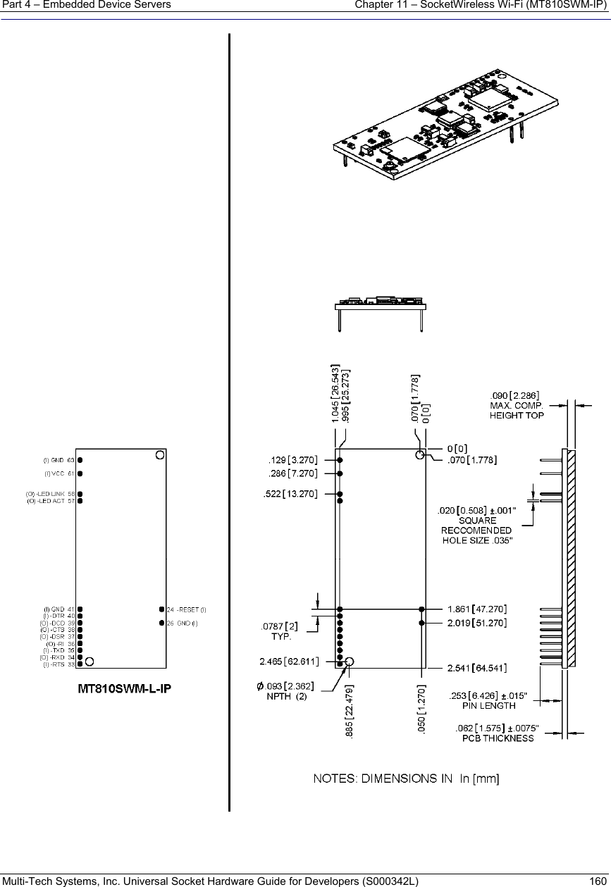
![Part 4 – Embedded Device Servers Chapter 11 – SocketWireless Wi-Fi (MT810SWM-IP) Multi-Tech Systems, Inc. Universal Socket Hardware Guide for Developers (S000342L) 161 Operating Conditions In Volts Parameter Minimum Maximum 3.3V = 3.15 3.3V = 3.45 Supply Range - Vcc 5V = 4.75 5V = 5.25 Absolute Maximum Rating Parameter Minimum Maximum Voltage at any signal pin GND - 0.3V Vcc + 0.3V DC Electrical Characteristics For 5V and 3.3V Units (Volts) Parameter Minimum Maximum GND 0.8V Digital Signal Input Low Level 2.0V Vcc Digital Signal Input High Level NA 0.4V Digital Signal Output Low Level 2.4V NA Digital Signal Output High Level GND 0.8V Reset (Low Active) Input Low 2.0V Vcc Reset (Low Active) Input High Digital Input Capacitance 5pf Power Measurements* MT810SWM-IP Measured Power at Input Voltage: 3.3 Volts Idle Typical Maximum Current (AMPS) 0.057 0.180 0.260 Watts 0.182 0.531 0.764 MT810SWM-IP Measured Power at Input Voltage: 5.00 Volts Idle Typical Maximum Current (AMPS) 0.056 0.193 0.260 Watts 0.274 0.897 1.196 * Multi-Tech Systems, Inc. recommends that the customer incorporate a 10% buffer into their power source when determining product load. Comment [DAR82]: The voltages came from Tom Fix on Sept 25, 2009. I put in the guide on 10/16/09.](https://usermanual.wiki/Multi-Tech-Systems/92U09G17825.User-Manual/User-Guide-1204041-Page-161.png)
![PART 4 – Embedded Device Servers Chapter 12 – SocketWireless Bluetooth (MTS2BTSMI) Multi-Tech Systems, Inc. Universal Socket Hardware Guide for Developers (S000342L) 166 SocketWireless Bluetooth Pin Out Note: The bolded, shaded pins are the active SocketWireless pins. Top View – SocketWireless Bluetooth Pin Out For pin descriptions, see the Universal Pin Out Descriptions in Chapter 1. DC Electrical Characteristics 5V Serial SocketWireless 5VDC Characteristics (VDD = 5V ± 0.25V) VDDMAX = 5.25V Inputs Input High Input Low –DTR (40), –TXD (35), –RTS (33) Min 2.0V Max 0.8V –RESET (24) Min 2.0V Max 0.8V Input Capacitance 15 pF Outputs Output High Output Low Current Drive –DCD (39), –CTS (38), –RI (36), –RXD (34) Min 4V / 2.4V Max 0.5V / 0.5V (5V / 3.3V) 3.2mA, 7.0mA for TXD 3.3V Serial SocketWireless 3.3VDC Characteristics (VDD = 3.3V ± 0.3V) VDDMAX = 3.6V Inputs Input High Input Low –DTR (40), –TXD (35), –RTS (33) Min 2.0V Max 0.8V –RESET (24) Min 2.0V Max 0.8V Input Capacitance 15 pF Outputs Output High Output Low Current Drive –DCD (39), –CTS (38), –RI (36), –RXD (34) Min 2.4V Max 0.5V / 0.5V (5V / 3.3V) 3.2mA, 7.0mA for TXD Comment [DAR83]: New one: 20501d1_BT_Mechanicaldimensions.gif Old one: 205001d1_mechanicalDimensions.bmp](https://usermanual.wiki/Multi-Tech-Systems/92U09G17825.User-Manual/User-Guide-1204041-Page-166.png)