Nokia Solutions and Networks T6FE1 PCS Licensed Transmitter User Manual 68P09262A58 C
Nokia Solutions and Networks PCS Licensed Transmitter 68P09262A58 C
UserManual.wiki
>
Nokia Solutions and Networks
>
T6FE1 User Manual
>
User Manual 2 of 3
Contents
1.
User Manual 1 of 3
2.
User Manual 2 of 3
3.
User Manual 3 of 3
User Manual 2 of 3
Navigation menu
Upload a User Manual
Namespaces
Wiki Guide
HTML
PDF
Info
Views
User Manual
Discussion / Help
Navigation
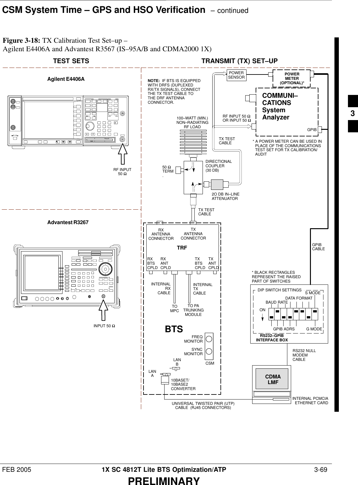

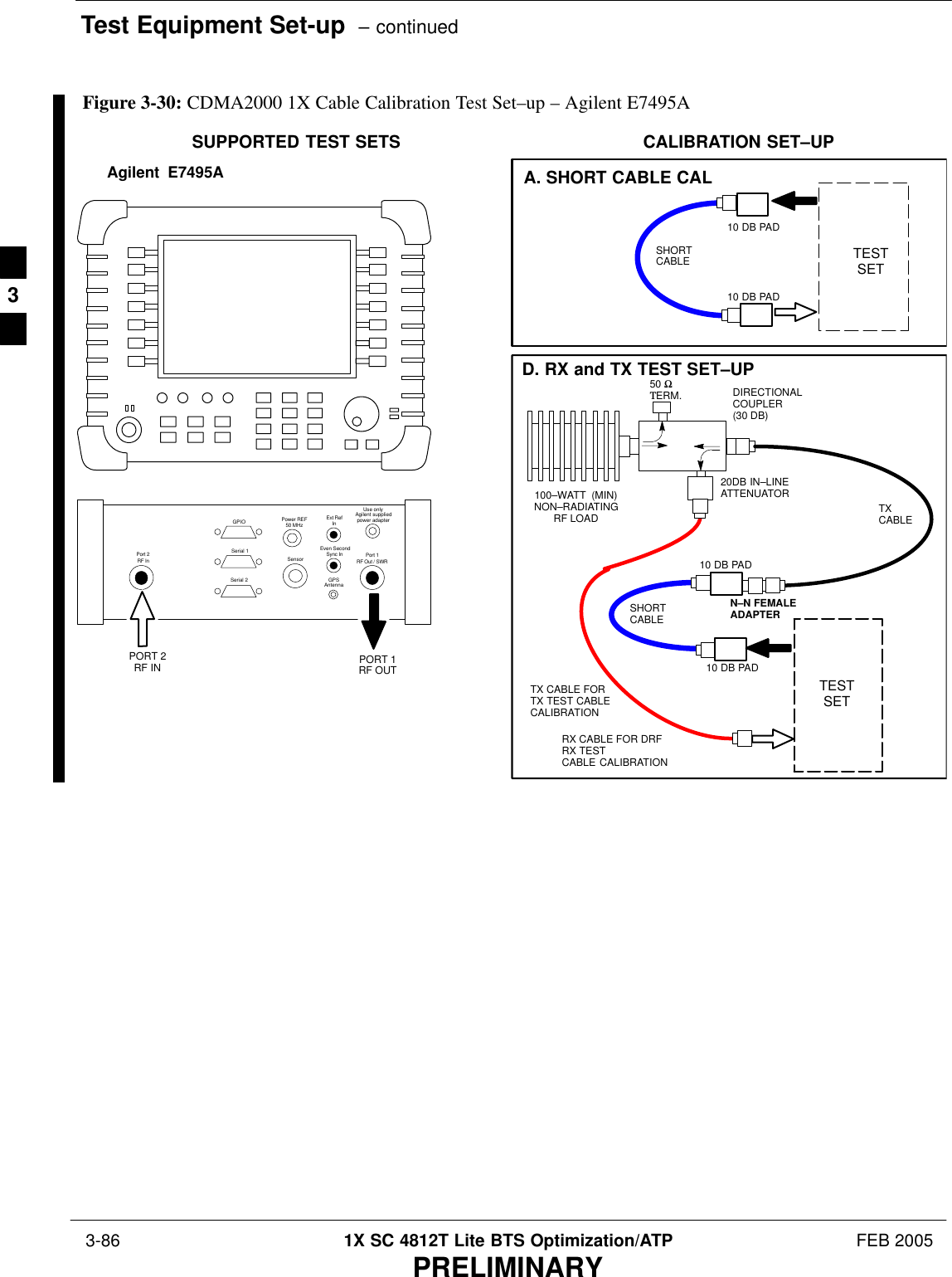
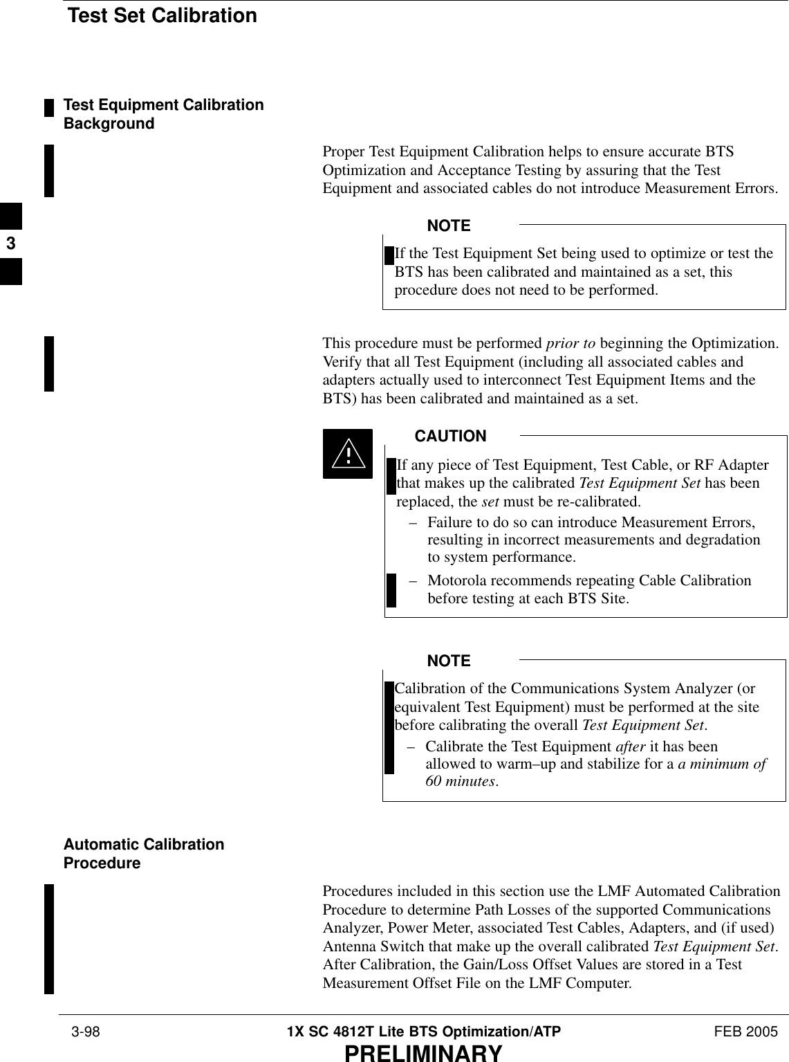
![Bay Level Offset Calibration – continued 3-114 1X SC 4812T Lite BTS Optimization/ATP FEB 2005PRELIMINARY– TX Filter or TX Filter Combiner– TX Filter/Filter Combiner–to–DRF/TRF Cable– DRF or TRFBLO Calibration Data FileDuring the Calibration Process, the LMF creates a Calibration (CAL)Data File where BLO Values are stored. After Calibration has beencompleted, these Offset Values must be downloaded to the BBX Cardsusing the LMF BLO Download Function. A detailed description of thefile organization and content is provided in the following paragraphs.Due to the size of the file, Motorola recommends printingout a copy of a bts–#.cal file and referring to it for thefollowing descriptions.NOTECAL File OrganizationThe CAL File is subdivided into three sections called “Slot Blocks”.These are:1. Slot[1] Block that contains the Calibration Data for the six PrimaryBBX Slots.2. Slot[20] Block that contains the Calibration Data for the RedundantBBX. Refer to Table 3-38.3. Slot[385] Block that contains the Calibration Data for the RFDS.BBX Slot Block PartsBBX Slot Blocks are further subdivided into the parts described in thefollowing paragraphs.Slot Block Header – Each BBX Slot Block has a Header Section (SlotHeader) that contains the following items.:SA Creation Date and Time – broken down into separate parameters of“createMonth”, “createDay”, “createYear”, “createHour”, and“createMin”.SThe number of Calibration Entries in the file – the“numBayLevelPts” Parameter. The parameter is fixed at 720 entriesfor SC4812 Series Frames. These 720 entries are combined to definethe 360 Calibration Points of the CAL File.SThe slot Block format parameter.Slot Block Bay Level Calibration Data – Each BBX Slot Block has aBay Level Calibration Data Section (BayLevelCal) that is organized as alarge flat array. The array is organized by Branch, SCCP Cage BBXSlot, and Calibration Entries. There are several ways to look at the array contents. Two different viewsare provided in the following to illustrate the significant features of“BayLevelCal” section content and organization:3](https://usermanual.wiki/Nokia-Solutions-and-Networks/T6FE1.User-Manual-2-of-3/User-Guide-520638-Page-93.png)
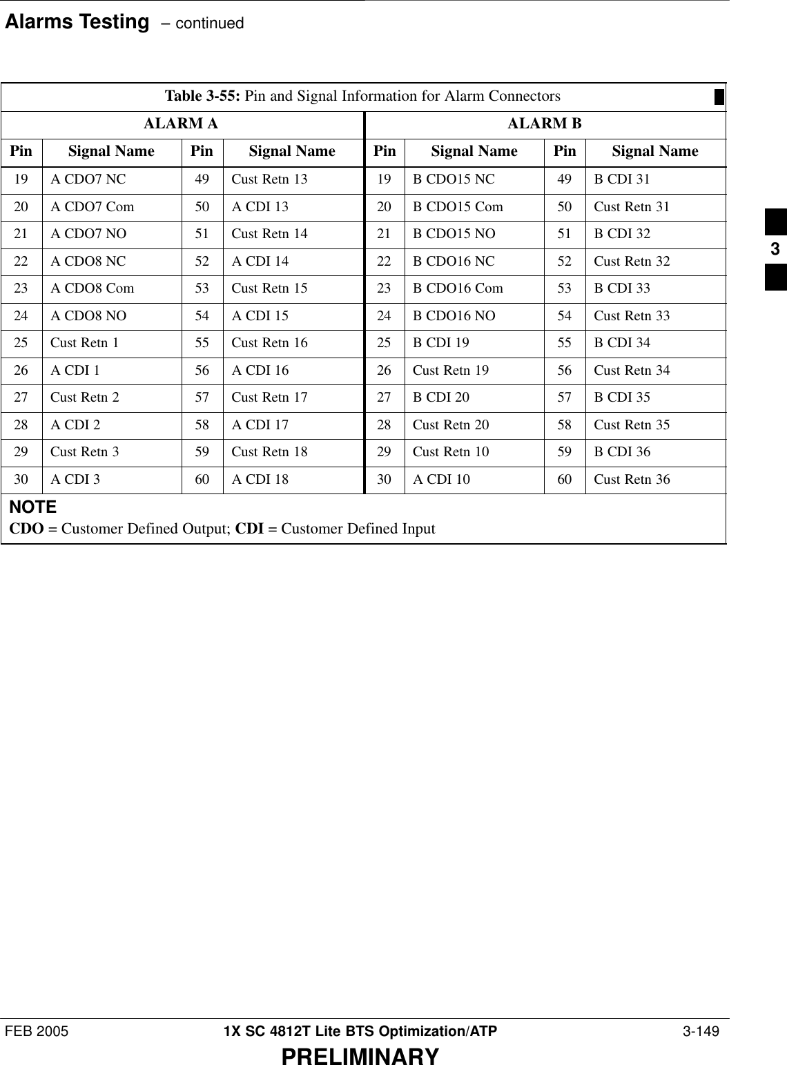
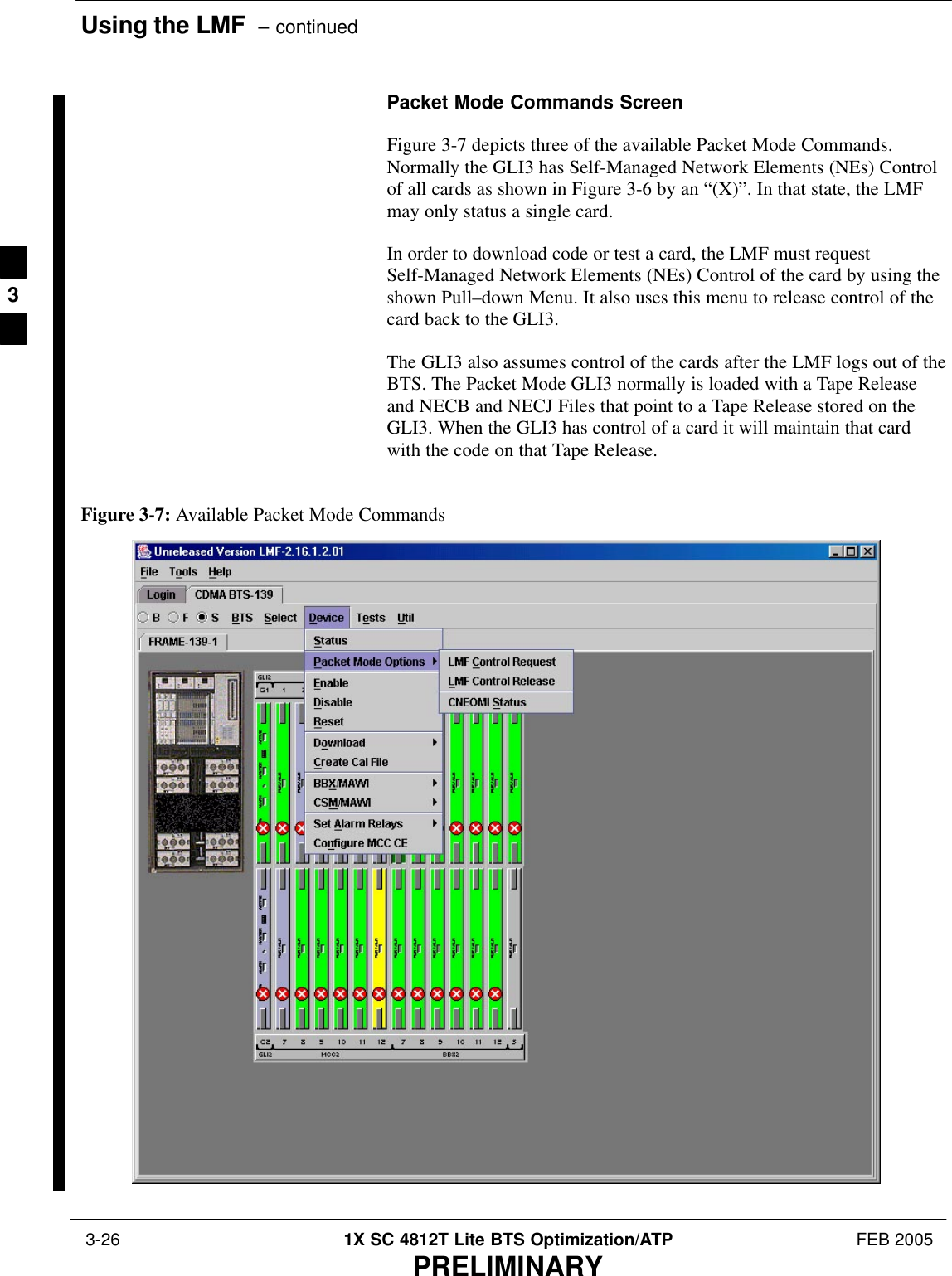
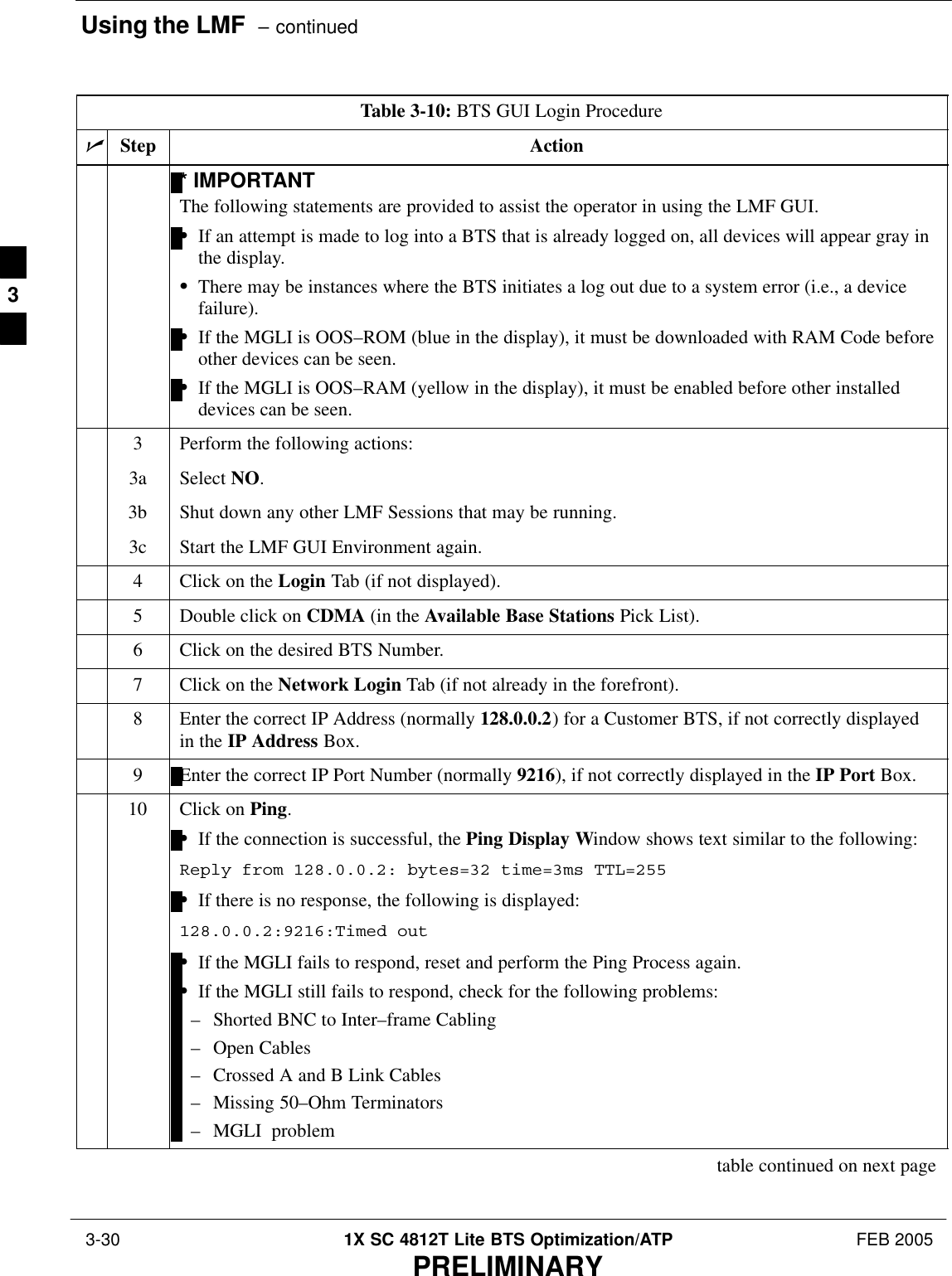
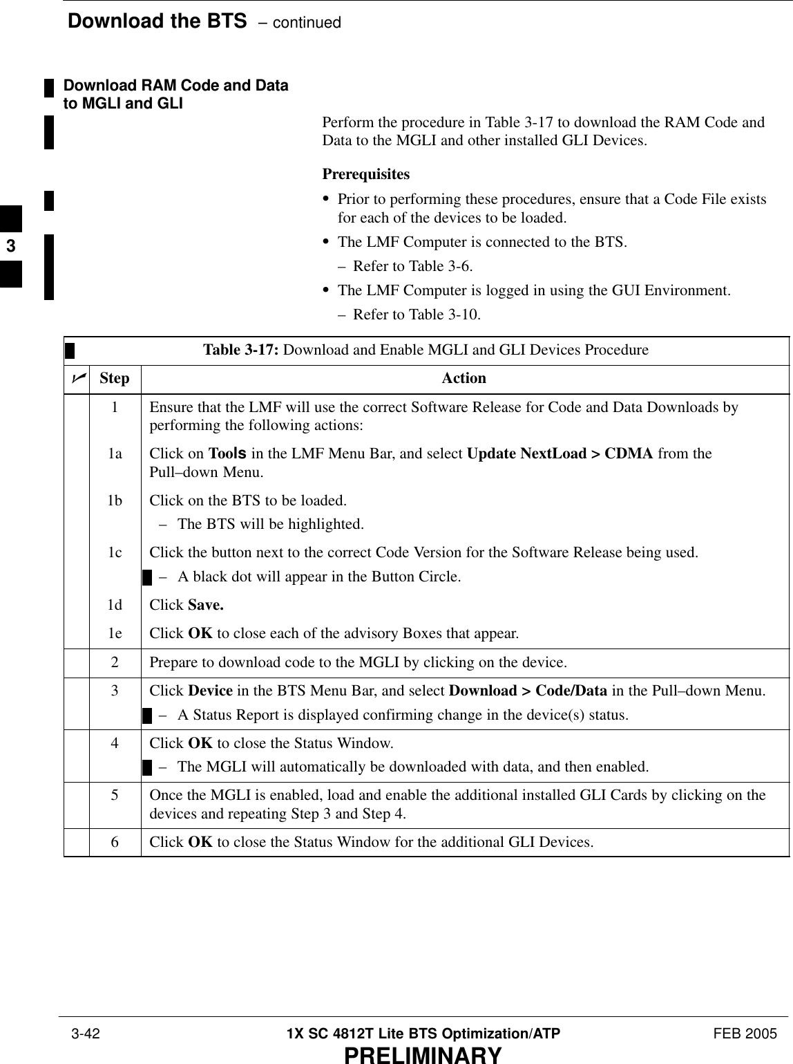
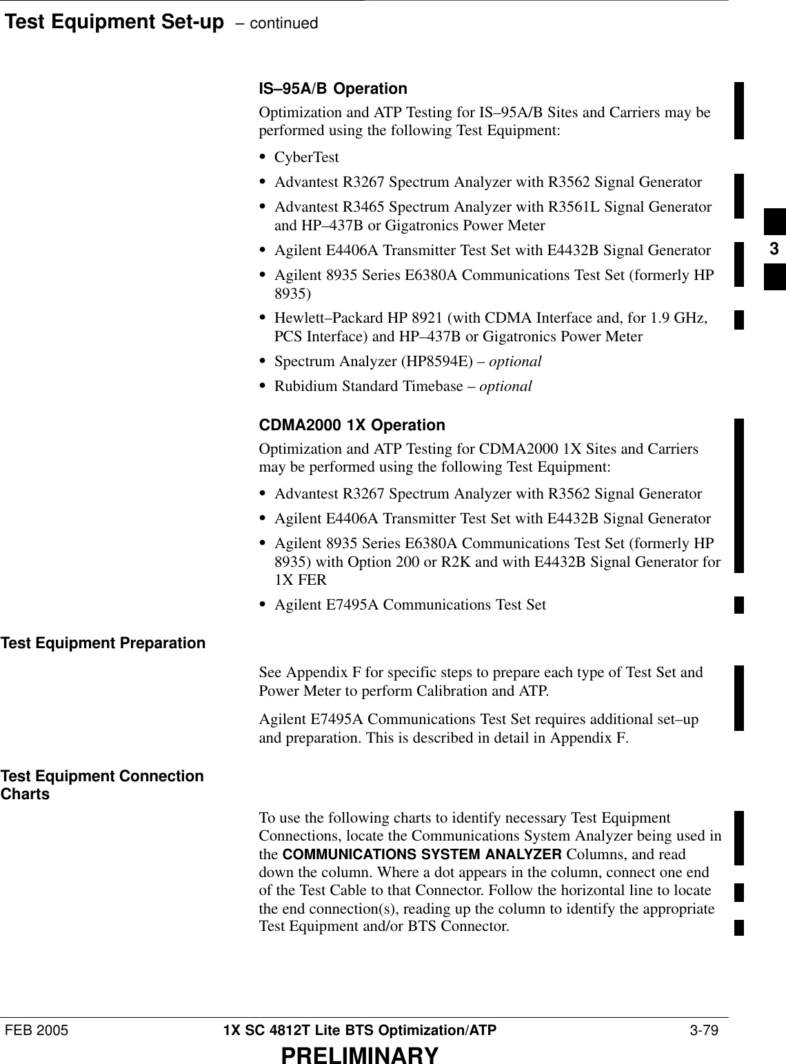
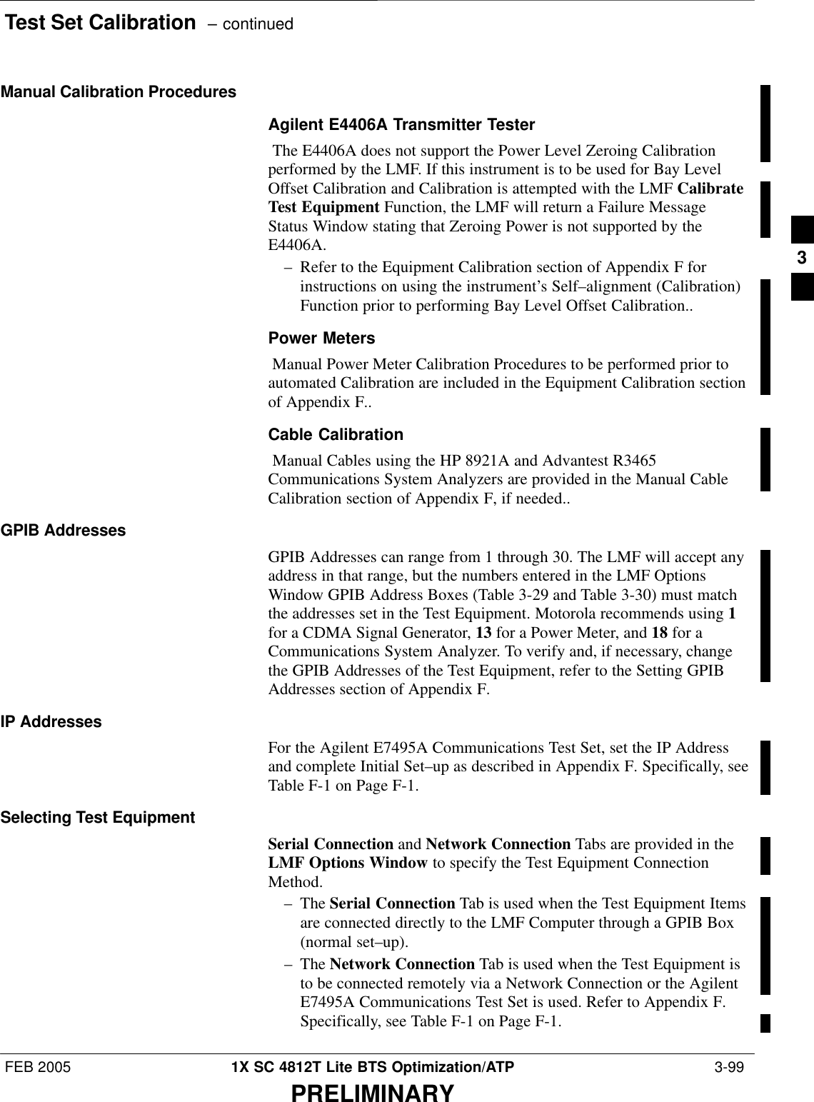
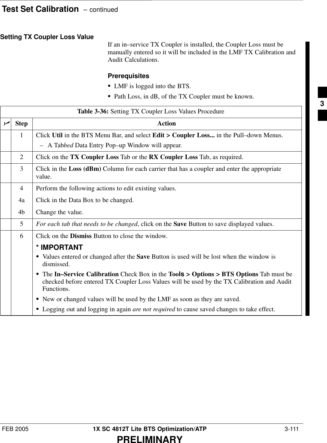
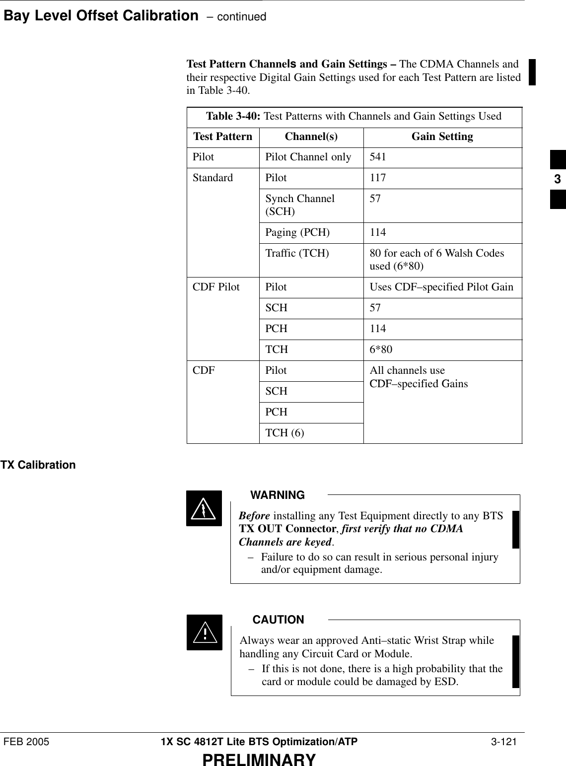
![Bay Level Offset Calibration – continuedFEB 2005 1X SC 4812T Lite BTS Optimization/ATP 3-115PRELIMINARYSThe first view of the array is shown in Table 3-37. This view showsthe three branches of the array (Transmit, Main Receive, andDiversity Receive Offsets, and the Calibration Entry ranges that applyto each.Table 3-37: BLO bts–#.cal File Array Branch AssignmentsRange Branch AssignmentC[1]–C[120] TransmitC[121]–C[240] No SC4812T Lite BLO Cal Point Entries (Default only)C[241]–C[360] ReceiveC[361]–C[480] No SC4812T Lite BLO Cal Point Entries (Default only)C[481]–C[600] Diversity ReceiveC[601]–C[720] No SC4812T Lite BLO Cal Point Entries (Default only)SThe second view of the array is shown in Table 3-38. This view showsthe assignment of Calibration Entries in each branch to each BBXSlot, Carrier, and Sectorization. Three sectors are allowed in anSC4812T Lite BTS Frame.Table 3-38: SC4812T Lite bts–#.cal File Array (by BBX/Sector)BBX Sectorization TX Branch RX Branch RX DiversityBranchSlot[1] (Primary BBX Cards 1 through 6)1 (Omni) C[1]–C[20] C[241]–C[260] C[481]–C[500]23–Sector,1st Carrier C[21]–C[40] C[261]–C[280] C[501]–C[520]31st CarrierC[41]–C[60] C[281]–C[300] C[521]–C[540]4 C[61]–C[80] C[301]–C[320] C[541]–C[560]53–Sector,2nd CarrierC[81]–C[100] C[321]–C[340] C[561]–C[580]62nd CarrierC[101]–C[120] C[341]–C[360] C[581]–C[600]C[121]–C[140] C[361]–C[380] C[601]–C[620]C[141]–C[160] C[381]–C[400] C[621]–C[640]Not Used in SC4812T Lite(CAL File Entries are Channel 0 withC[161]–C[180] C[401]–C[420] C[641]–C[660](CAL File Entries are Channel 0 withDefault Power Set Level) C[181]–C[200] C[421]–C[440] C[661]–C[680])C[201]–C[220] C[441]–C[460] C[681]–C[700]C[221]–C[240] C[461]–C[480] C[701]–C[720]table continued next page3](https://usermanual.wiki/Nokia-Solutions-and-Networks/T6FE1.User-Manual-2-of-3/User-Guide-520638-Page-94.png)
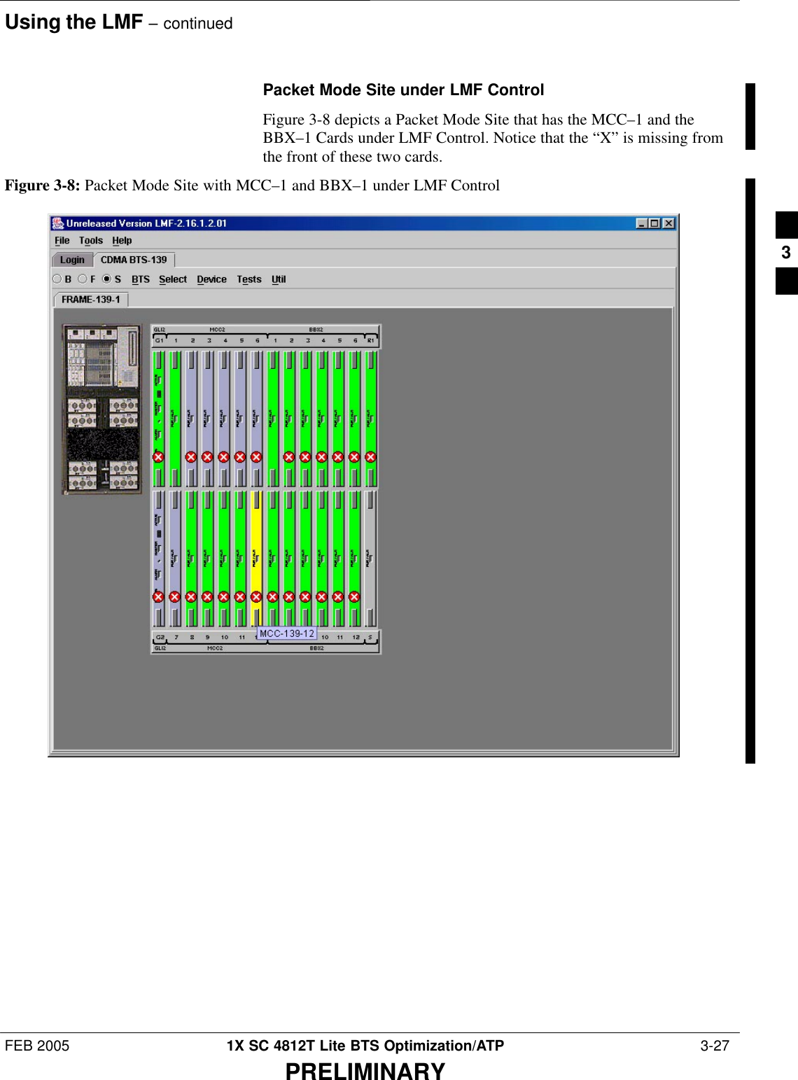
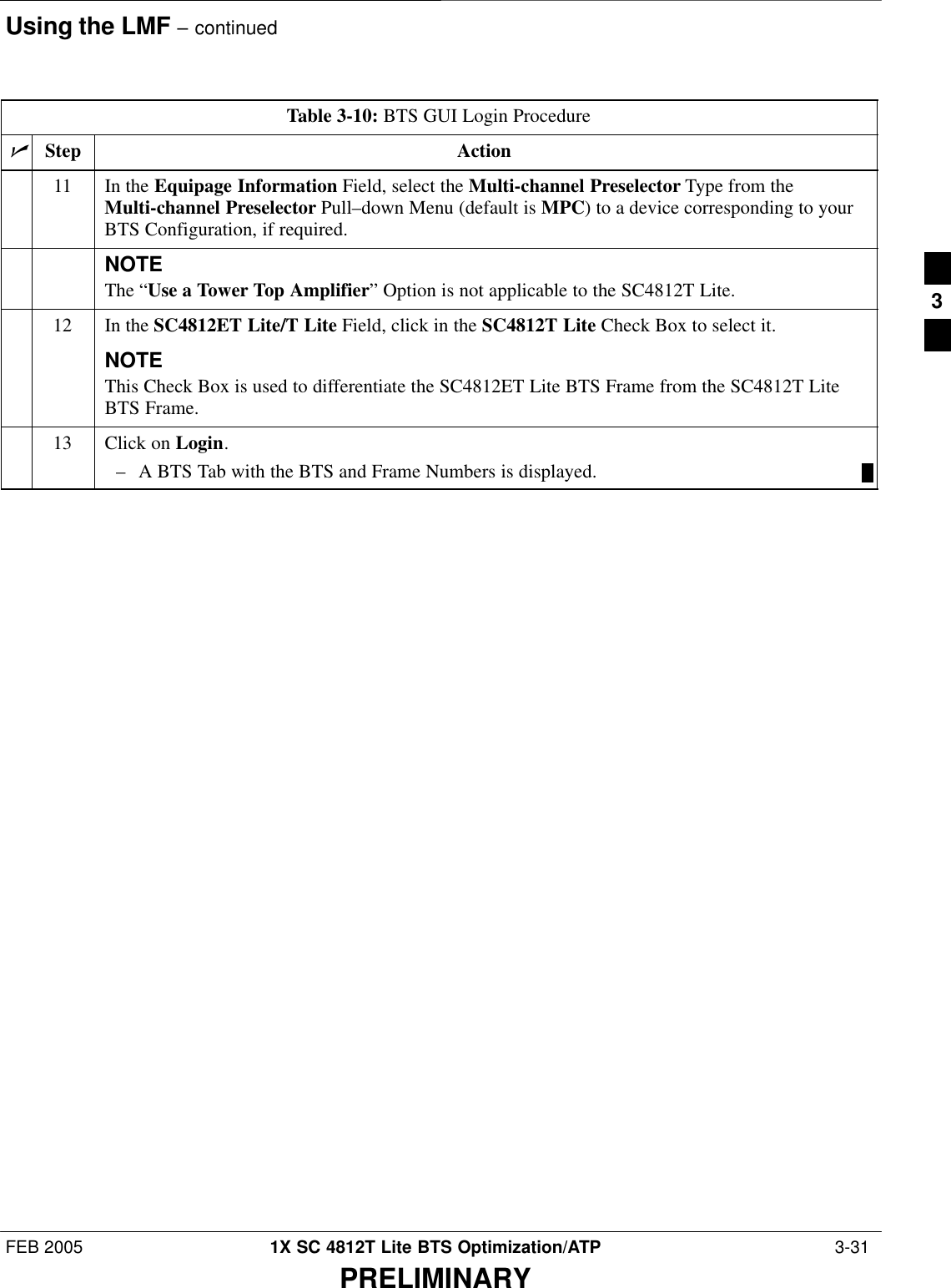
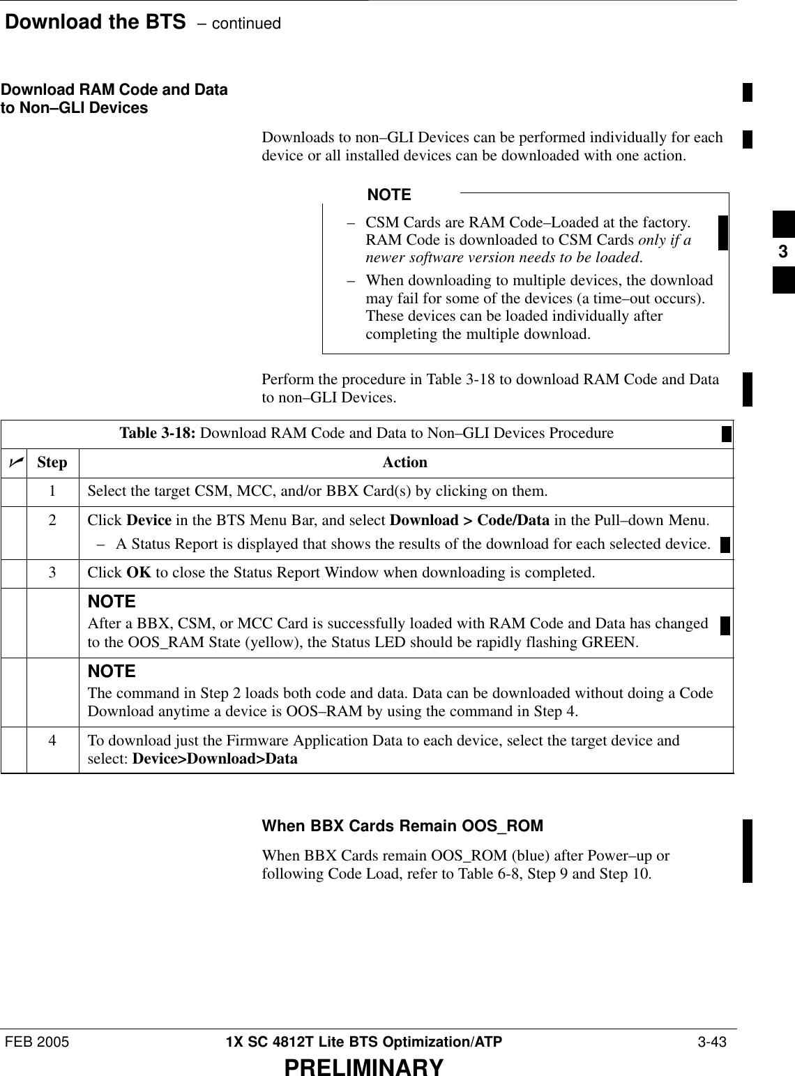
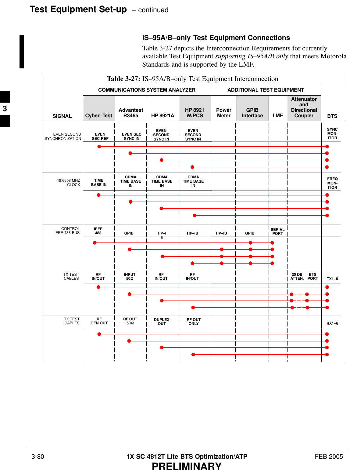
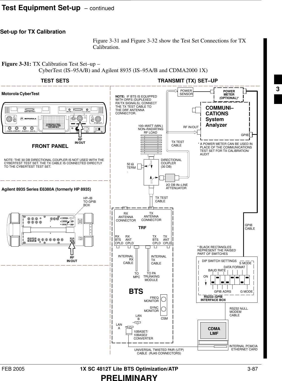
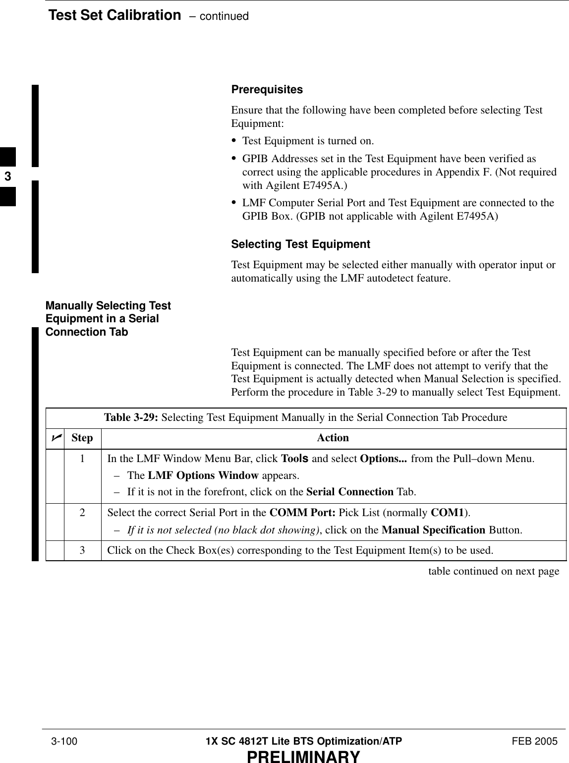
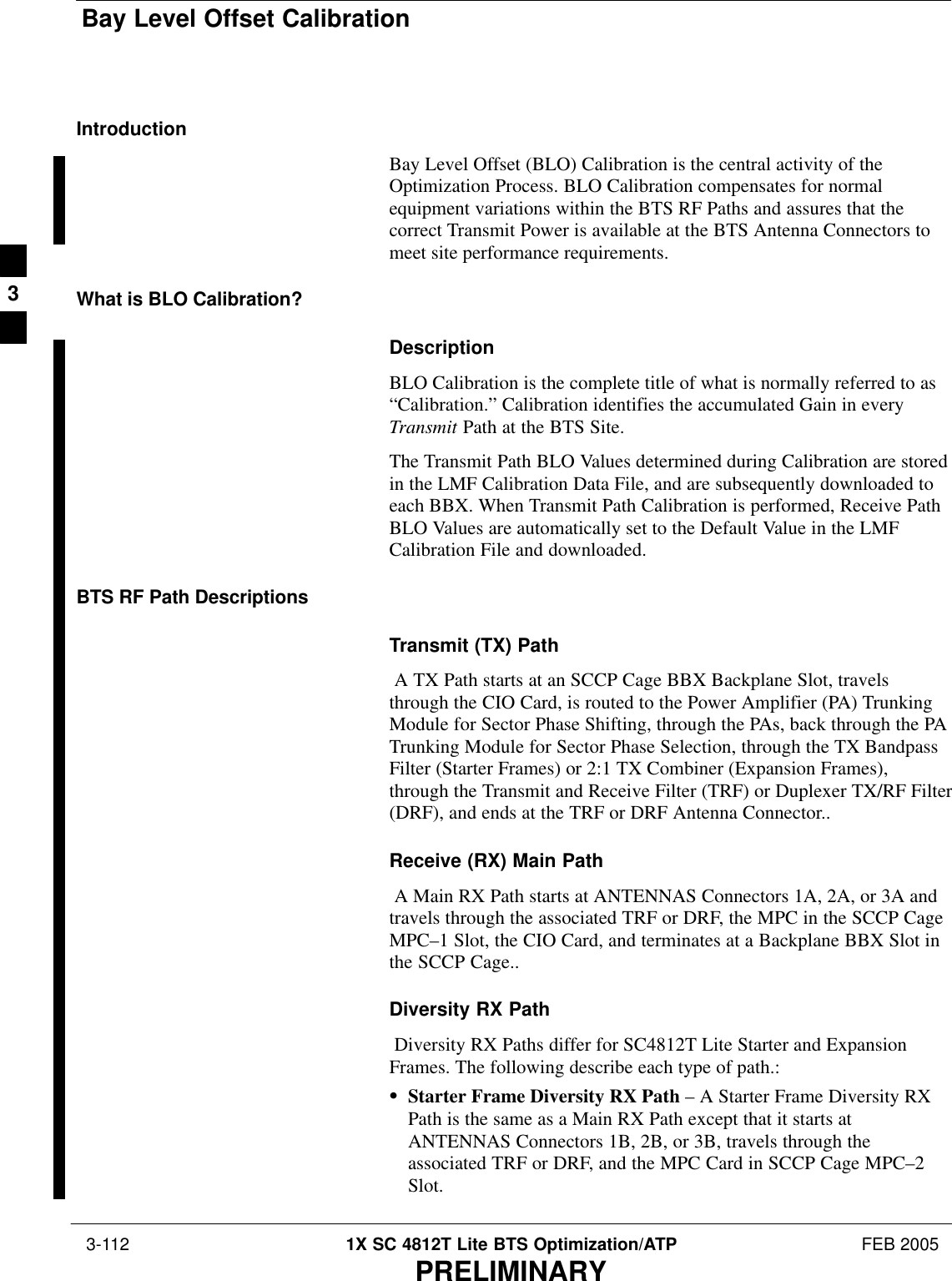
![Bay Level Offset Calibration – continued 3-116 1X SC 4812T Lite BTS Optimization/ATP FEB 2005PRELIMINARYTable 3-38: SC4812T Lite bts–#.cal File Array (by BBX/Sector)BBX RX DiversityBranchRX BranchTX BranchSectorizationSlot[20] (Redundant BBX–R1)1 (Omni) C[1]–C[20] C[241]–C[260] C[481]–C[500]23–Sector,1st CarrierC[21]–C[40] C[261]–C[280] C[501]–C[520]31st CarrierC[41]–C[60] C[281]–C[300] C[521]–C[540]4 C[61]–C[80] C[301]–C[320] C[541]–C[560]53–Sector,2nd CarrierC[81]–C[100] C[321]–C[340] C[561]–C[580]62nd CarrierC[101]–C[120] C[341]–C[360] C[581]–C[600]C[121]–C[140] C[361]–C[380] C[601]–C[620]C[141]–C[160] C[381]–C[400] C[621]–C[640]Not Used in SC4812T Lite(CAL File Entries are Channel 0 withC[161]–C[180] C[401]–C[420] C[641]–C[660](CAL File Entries are Channel 0 withDefault Power Set Level) C[181]–C[200] C[421]–C[440] C[661]–C[680])C[201]–C[220] C[441]–C[460] C[681]–C[700]C[221]–C[240] C[461]–C[480] C[701]–C[720] SWhen referring to the CAL File Printout and Table 3-38, it can be seenthat there is one BBX Slot per sector with 20 “Calibration Entries” perBBX (sector) for each branch. Two Calibration Entries define a single“Calibration Point;” therefore there are ten Calibration Points in eachbranch for each BBX.– The first Calibration Entry for a Calibration Point (all odd entries)identifies the CDMA Channel (frequency) where the BLO ismeasured.– The second Calibration Entry (all even entries) is the Power SetLevel (PwrLvlAdj) for that frequency. The valid range for“PwrLvlAdj” is from 2500 to 27500 (2500 corresponds to–125 dBm and 27500 corresponds to +125 dBm).– The ten Calibration Points for each Slot–Branch Combination mustbe stored in order of increasing frequency. If less than ten points(frequencies) are calibrated, the BLO Data for the highest frequencycalibrated is written into the remainder of the ten points for thatSlot–Branch.3](https://usermanual.wiki/Nokia-Solutions-and-Networks/T6FE1.User-Manual-2-of-3/User-Guide-520638-Page-95.png)
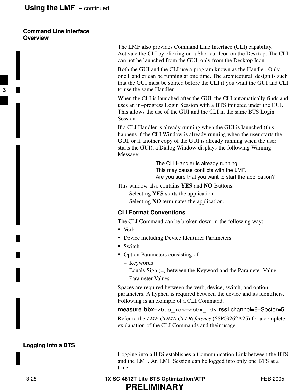
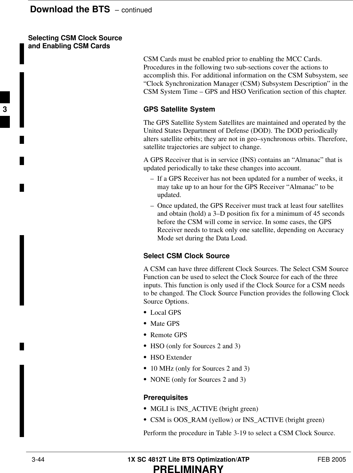
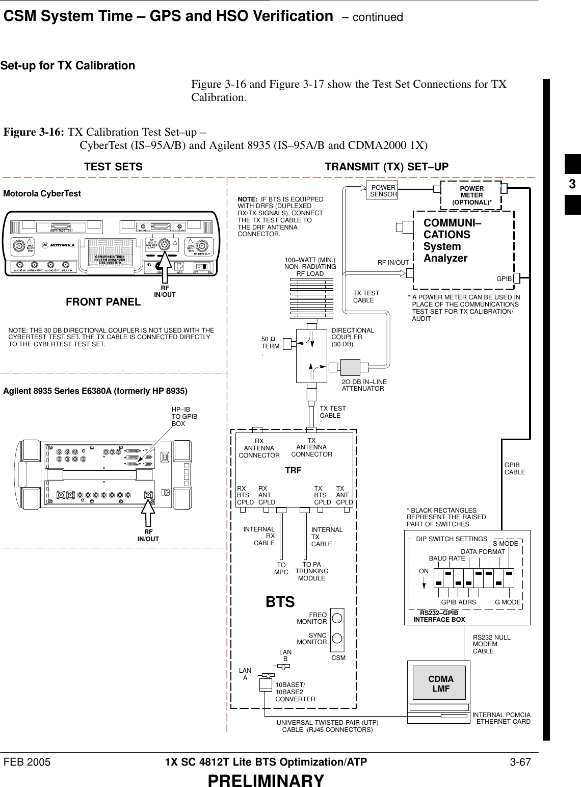
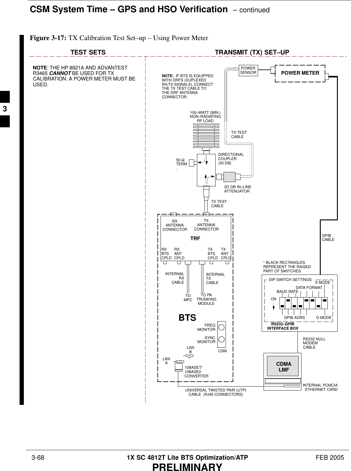
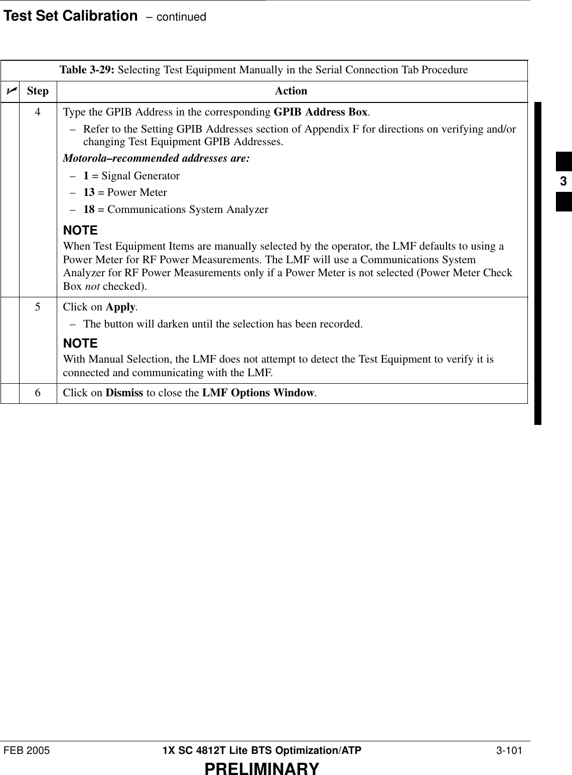
![Bay Level Offset Calibration – continuedFEB 2005 1X SC 4812T Lite BTS Optimization/ATP 3-117PRELIMINARYExample:C[1]=384 (Odd Cal Entry)C[2]=19102 (Even Cal Entry)C[3]=777 (Odd Cal Entry)C[4]=19086 (Even Cal Entry)C[19]=777 (Odd Cal Entry)C[20]=19086 (Even Cal Entry)...= 1 “Calibration Point”= 1 “Calibration Point”= 1 “Calibration Point”In the example above, BLO was measured at only two frequencies(Channels 384 and 777) for SCCP BBX–1 Slot Transmit (Table 3-38).The BLO Data for the highest frequency measured (Channel 777) willbe written to the remaining eight Transmit Calibration Points (definedby Entry C[5] through Entry C[20]) for BBX–1.Slot Block Temperature Compensation – Each BBX Slot Block alsohas a Temperature Compensation Data Section (TempLevelCal) wherePower Level Compensation Factors for Temperature Variations arestored..CAL File and BLO Data DownloadWhen BLO Data is downloaded to the BBX Cards after Calibration, thedata is downloaded to the devices in the order it is stored in the CALFile. TX Calibration Data (Entries C[1] through C[60]) are sent first.Data for the ten BBX Slot 1 Calibration Points (Entries C[1] throughC[20]) are sent initially, followed by data for the ten BBX Slot 2Calibration Points (Entries C[21] through C[40]), and so on. The RXCalibration Data is sent next in BBX Slot Sequence, followed by the RXDiversity Calibration Data.Test Equipment Set–up forRF Path CalibrationPerform the procedure in Table 3-39 and refer as needed to Figure 3-16or Figure 3-17 to Set–up Test Equipment.Table 3-39: Set–up Test Equipment for RF Path Calibration ProcedurenStep Action1If it has not already been done, refer to the procedure in Table 3-6 (on Page 3-18) to interface theLMF Computer Terminal to the BTS Frame LAN A Connector.2If it has not already been done, refer to Table 3-10 (on Page 3-29) to start a GUI LMF Session.3If required, calibrate the Test Equipment per the procedure in Table 1-4.table continued on next page3](https://usermanual.wiki/Nokia-Solutions-and-Networks/T6FE1.User-Manual-2-of-3/User-Guide-520638-Page-96.png)
![RFDS Set–up and Calibration – continuedFEB 2005 1X SC 4812T Lite BTS Optimization/ATP 3-131PRELIMINARYTable 3-45: RFDS Parameter Settings ProcedurenActionStep5c Click on Device in the BTS Menu Bar, and select Disable from the Pull–down Menu.– A Status Report Window shows the status of the operation.5d When the operation is complete, click OK to close the Status Report Window.5e Click on the MGLI [now OOS_RAM (yellow)].5f Click on Device in the BTS Menu Bar, and select Download > Data from the Pull–down Menus.– A Status Report Window shows the status of the download.NOTESelected devices do not change color when data is downloaded.5g Click OK to close the Status Report Window.5h Click on the MGLI.5i Click on Device in the BTS Menu Bar, and select Enable from the Pull–down Menu.– A Status Report Window shows the status of the operation.5j When the operation is complete, click OK to close the Status Report Window.! CAUTIONWhen the MGLI changes to INS_ACTIVE, data will automatically be downloaded to the RFDS.– During this process, the RFDS LED will slowly begin flashing red and green forapproximately 2–3 minutes.–DO NOT attempt to perform any functions with the RFDS until the LED remains steadygreen.5k Re–seat the Redundant GLI Card into its Backplane Connector and lock it in place with theEjector Tabs.5l Once the Redundant GLI initializes, download data to it by performing the following actions:– Select the card.– Click Device in the BTS Menu Bar.– Select Download > Data from the Pull–down Menu.6Any MCC Cards that were INS_ACTIVE when the MGLI was disabled must be disabled,downloaded with data, and re–enabled as follows:6a Select the devices to be reset.– Click on them.or– Choose Select from the BTS Menu Bar and click on MCC Cards in the Pull–down Menu.6b In the BTS Menu Bar, click on Device and select Disable from the Pull–down Menu.– A Status Report Window shows the status of the operation.table continued on next page3](https://usermanual.wiki/Nokia-Solutions-and-Networks/T6FE1.User-Manual-2-of-3/User-Guide-520638-Page-110.png)
![RFDS Set–up and Calibration – continued 3-132 1X SC 4812T Lite BTS Optimization/ATP FEB 2005PRELIMINARYTable 3-45: RFDS Parameter Settings ProcedurenActionStep6c Click OK to close the Status Report Window.6d Repeat Step 6a to select the MCC Cards.6e Click on Device in the BTS Menu Bar and select Download > Data from the Pull–down Menu.– A Status Report Window shows the status of the download.NOTESelected devices do not change color when data is downloaded.6f Click on OK to close the Status Report Window.6g When data download is complete, enable the MCC Cards by performing the procedure inTable 3-21.7Click on the RFDS Tab.8Status the RFDS TSU by performing the following actions.8a Click on the SUA to select it.8b Click on TSU in the BTS Menu Bar, and select Status TSU from the Pull–down Menu.– A Status Report shows the software Version Number for the TSIC and SUA.8c Click OK to close the Status Report Window.* IMPORTANTIf the LMF Displays an Error Message, check the following:SEnsure that the AMR Cable from the BTS to the RFDS is connected correctly.SVerify that the RFDS has power.SVerify that the RFDS Status LED is green.SVerify that the entries in the RFDS Fields of the bts–#.CDF File are correct.– Refer to Step 1.SStatus the MGLI and ensure it is communicating (by Ethernet) with the LMF, and is in theproper state [INS_ACTIVE (bright green)]. 3](https://usermanual.wiki/Nokia-Solutions-and-Networks/T6FE1.User-Manual-2-of-3/User-Guide-520638-Page-111.png)
![RFDS Set–up and Calibration – continued 3-136 1X SC 4812T Lite BTS Optimization/ATP FEB 2005PRELIMINARYSet RFDS Configuration DataIf an RFDS is installed, the RFDS Configuration Data must be manuallyentered.PrerequisiteSLMF is logged into the BTSThe entered antenna# index numbers must correspond tothe antenna# index numbers used in the Antenna Maps.NOTEPerform the procedure in Table 3-49 to set RFDS Configuration Data.Table 3-49: Set RFDS Configuration Data ProcedurenStep Action1Click on Util in the BTS Menu Bar, and select Edit > RFDS Configuration... from thePull–down Menus.–A Tabbed Data Entry Pop–up Window will appear.2In the Data Entry Pop–up Window, click on the TX RFDS Configuration or RX RFDSConfiguration Tab, as required.3To add a new Antenna Number, perform the following actions.3a Click on the Add Row Button.3b Click in the Antenna #, Cal Antenna, Scap Antenna, or Populate [Y/N] Columns, as required.3c Enter the desired data.4To edit existing values click in the Data Box to be changed and change the value.NOTERefer to the CDMA Help > Utility Menu > Edit–RFDS Configuration... section of LMF Helpfunction on–line documentation for RFDS Configuration Data examples.5To delete a row, click on the row and then click on the Delete Row Button.6For each tab that needs to be changed, click on the Save Button to save the displayed values.7Click on the Dismiss Button to close the window.NOTESValues entered or changed after the Save Button was used will be lost when the window isdismissed.– Entered values will be used by the LMF as soon as they are saved.SIt is not necessary to log out and log back into the LMF for changes to take effect. 3](https://usermanual.wiki/Nokia-Solutions-and-Networks/T6FE1.User-Manual-2-of-3/User-Guide-520638-Page-115.png)
![RFDS Set–up and Calibration – continuedFEB 2005 1X SC 4812T Lite BTS Optimization/ATP 3-137PRELIMINARYRFDS CalibrationThe RFDS Calibration option is used to calibrate the RFDS TX and RXPaths.TX Path CalibrationFor a TX Antenna Path Calibration, the BTS XCVR is keyed at apre–determined Power Level and the BTS Power Output Level ismeasured by the RFDS. The Power Level is then measured at the TXAntenna Directional Coupler by the power measuring Test EquipmentItem being used (Power Meter or Analyzer).– The difference (Offset) between the Power Level at the RFDS andthe Power Level at the TX Antenna Directional Coupler is used asthe TX RFDS Calibration Offset Value.RX Path CalibrationFor an RX Antenna Path Calibration, the RFDS is keyed at apre–determined Power Level and the Power Input Level is measured bythe BTS BBX. A CDMA signal at the same Power Level measured bythe BTS BBX is then injected at the RX antenna Directional Coupler bythe Communications System Analyzer.– The difference (Offset) between the RFDS–keyed Power Level andthe Power Level measured at the BTS BBX is the RFDS RXCalibration Offset Value.RFDS Calibration and the CAL File The TX and RX RFDS Calibration Offset Values are written to the CALFile in the Slot[385] Block.TSIC Channel Frequency For each RFDS TSIC, the Channel Frequency is determined at thelower third and upper third of the appropriate band using the frequencieslisted in Table 3-50..Table 3-50: RFDS TSIC Calibration Channel FrequenciesSystem Channel Calibration Points800 MHz (A and B) 341 and 6821.9 GHz 408 and 791Before installing any Test Equipment directly to any TXOUT Connector, verify that there are no CDMAChannels keyed.– Failure to do so can result in serious personal injuryand/or equipment damage.WARNING3](https://usermanual.wiki/Nokia-Solutions-and-Networks/T6FE1.User-Manual-2-of-3/User-Guide-520638-Page-116.png)