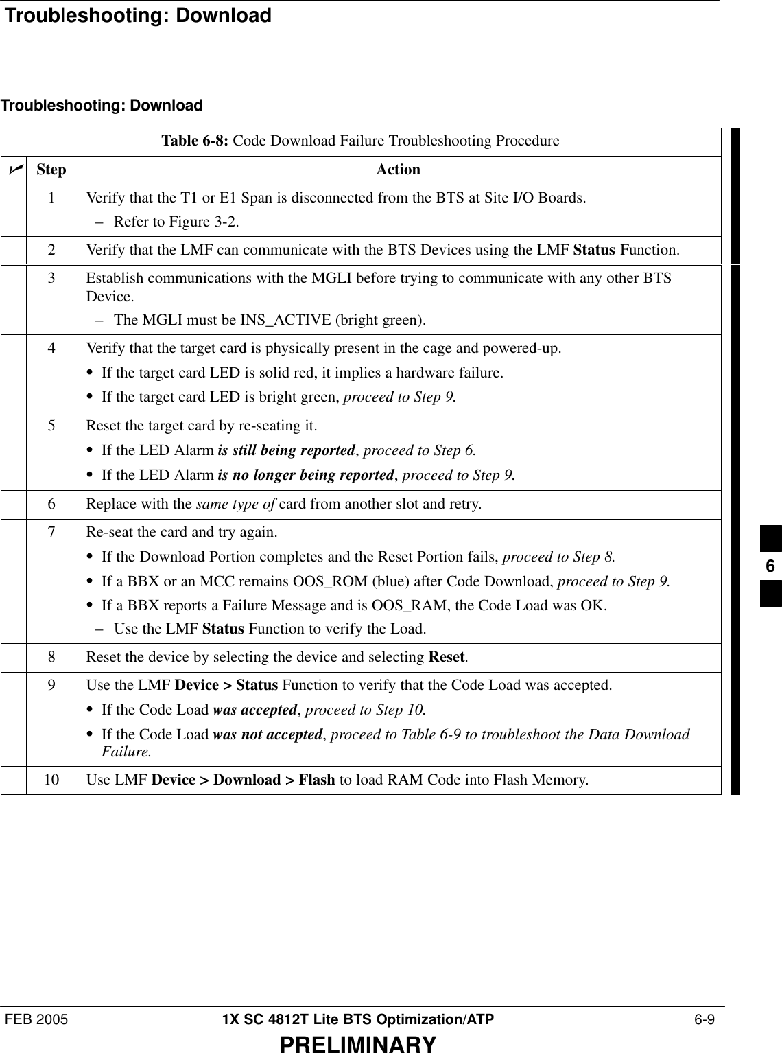
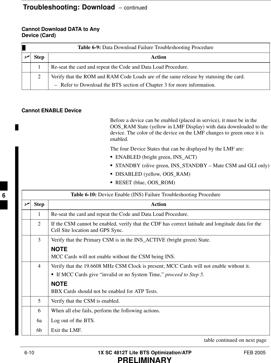
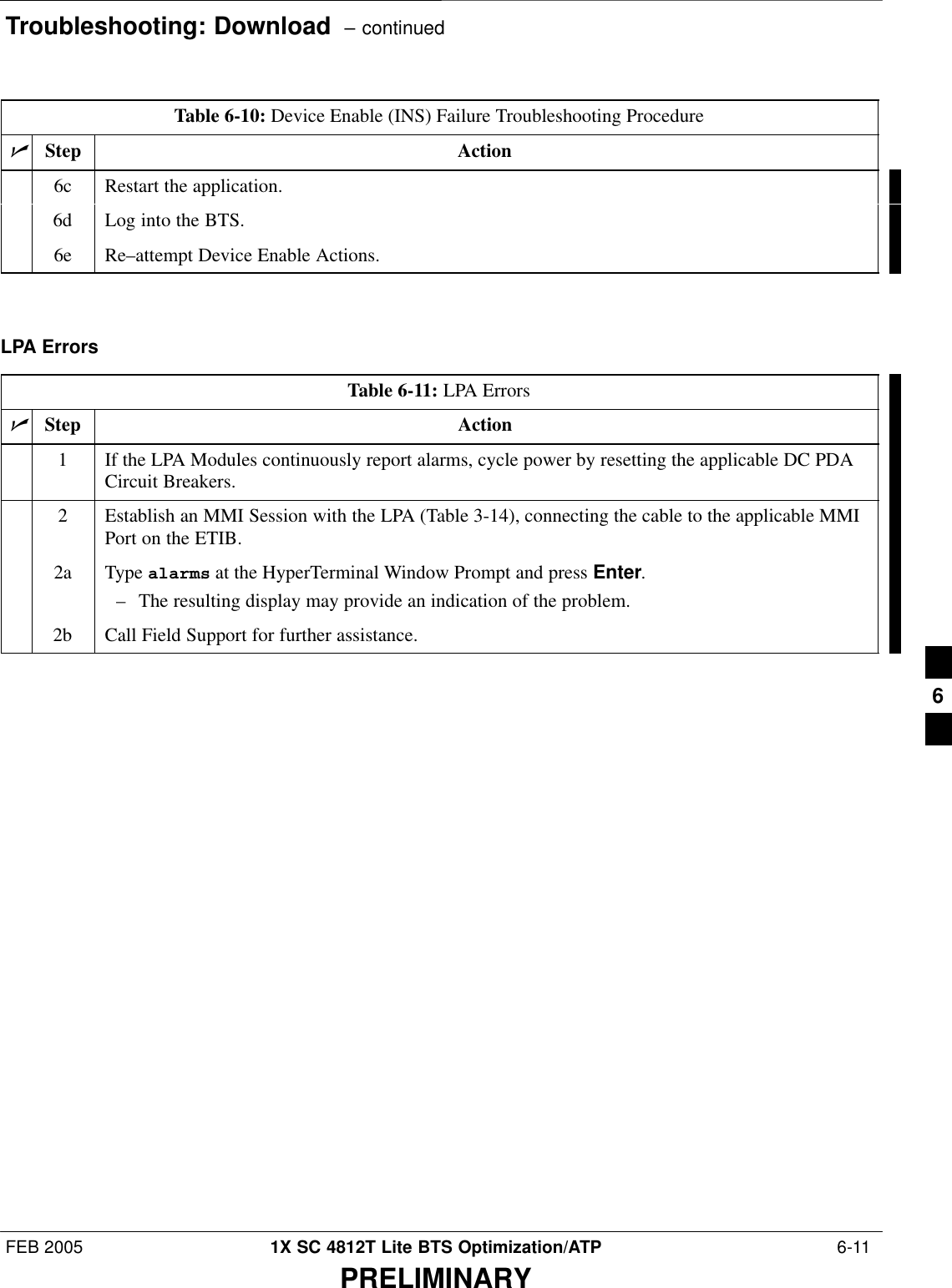
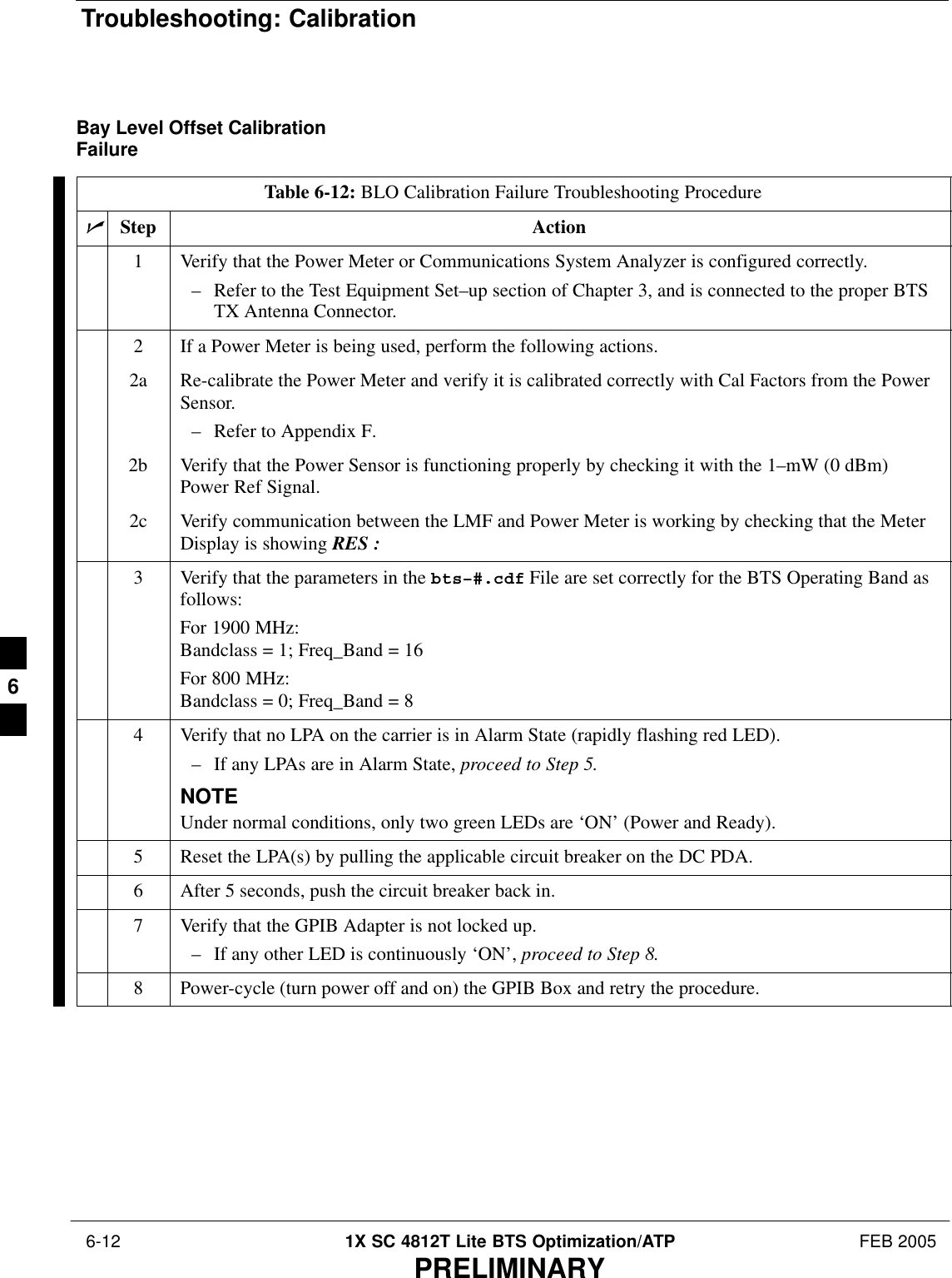
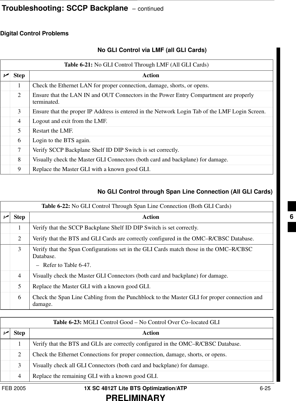
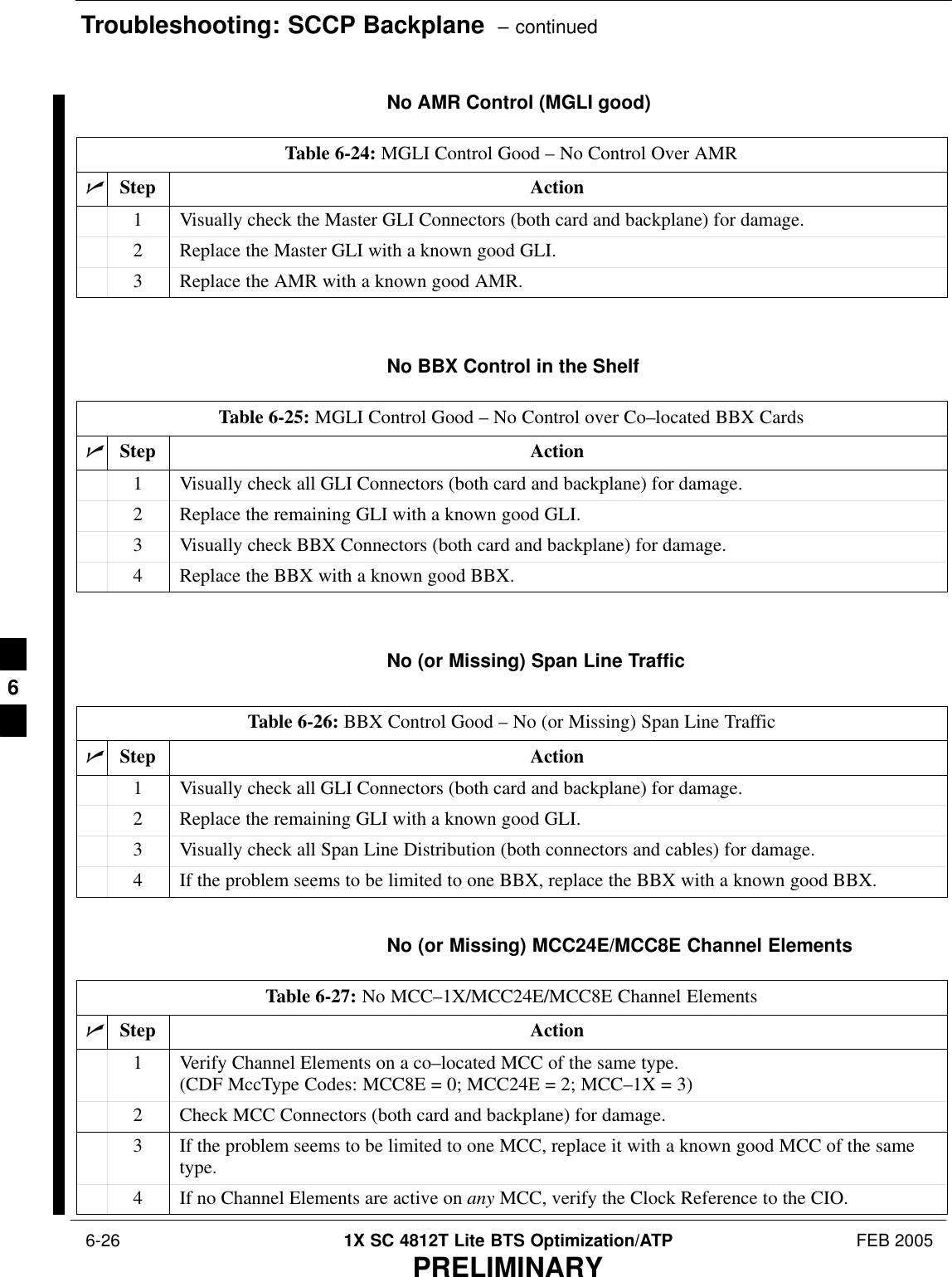
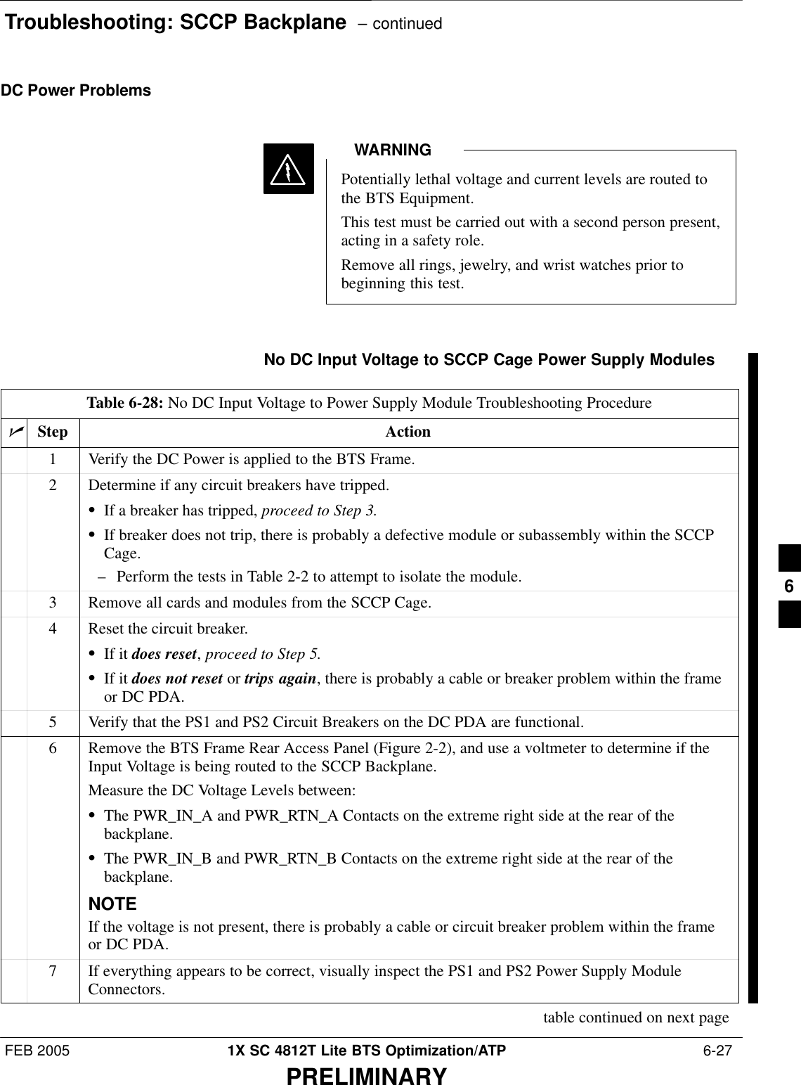
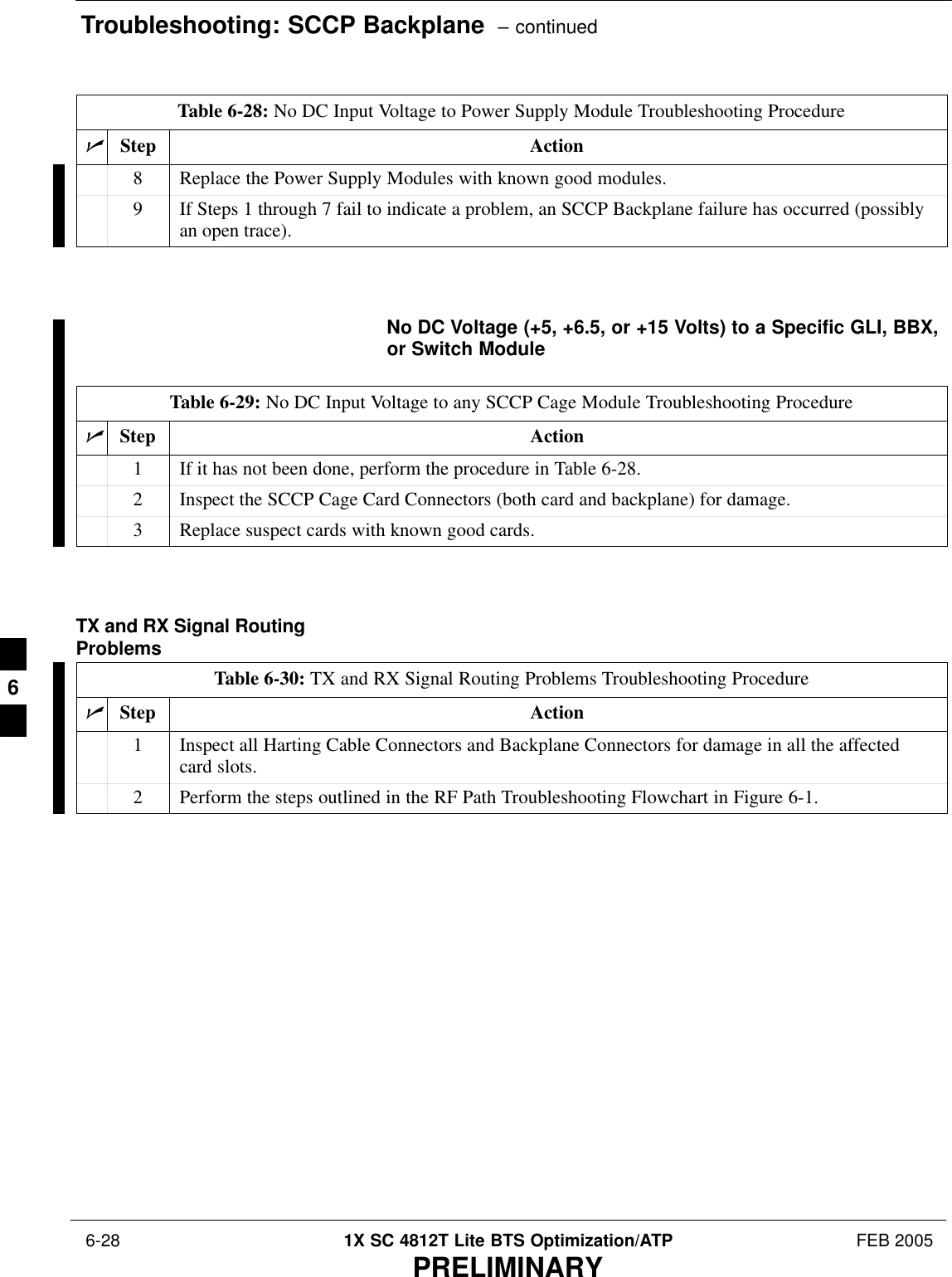
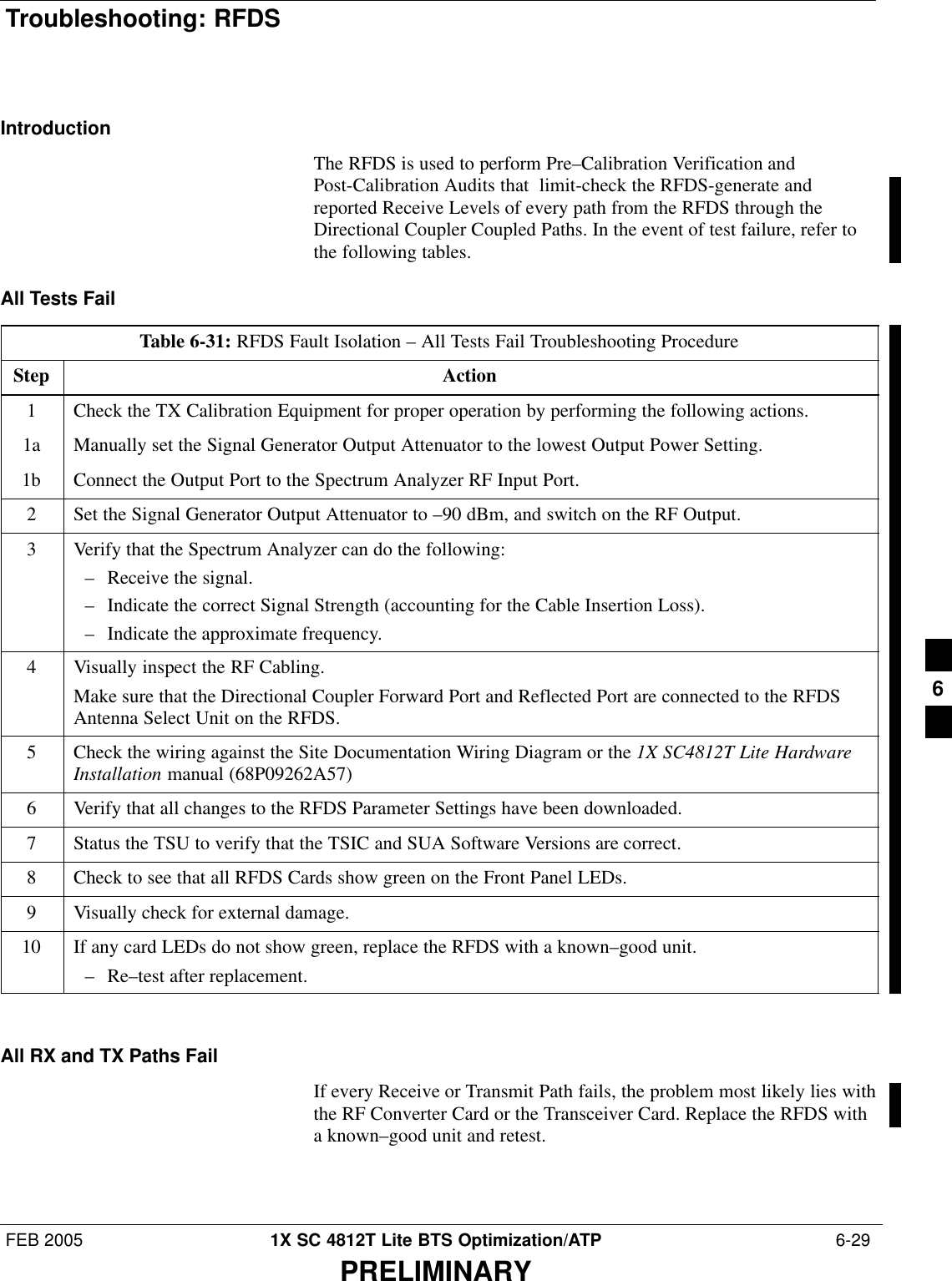
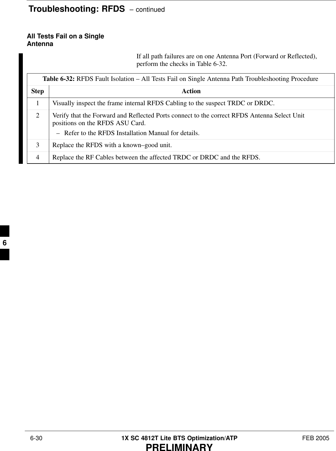
Nokia Solutions and Networks T6FE1 PCS Licensed Transmitter User Manual 68P09262A58 C
Nokia Solutions and Networks PCS Licensed Transmitter 68P09262A58 C
UserManual.wiki
>
Nokia Solutions and Networks
>
T6FE1 User Manual
>
User Manual 3 of 3
Contents
1.
User Manual 1 of 3
2.
User Manual 2 of 3
3.
User Manual 3 of 3
User Manual 3 of 3
Navigation menu
Upload a User Manual
Namespaces
Wiki Guide
HTML
PDF
Info
Views
User Manual
Discussion / Help
Navigation
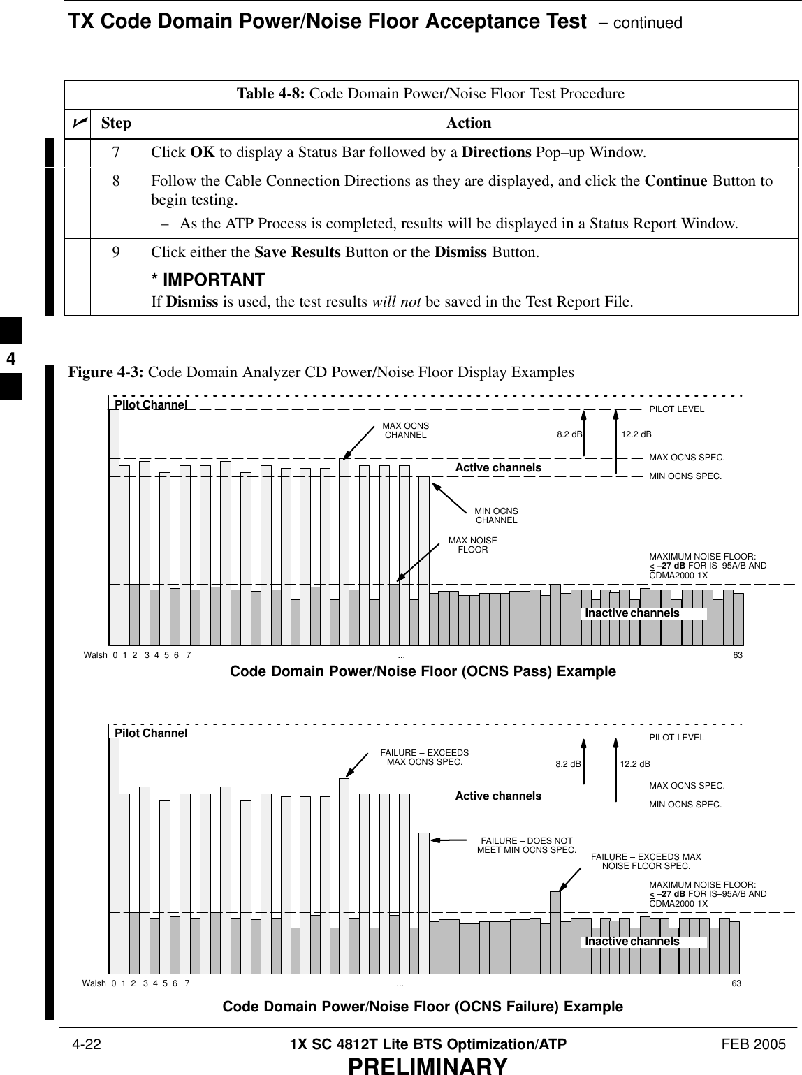
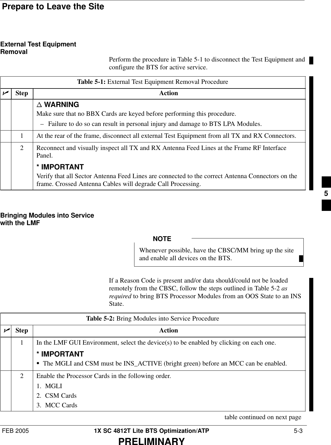
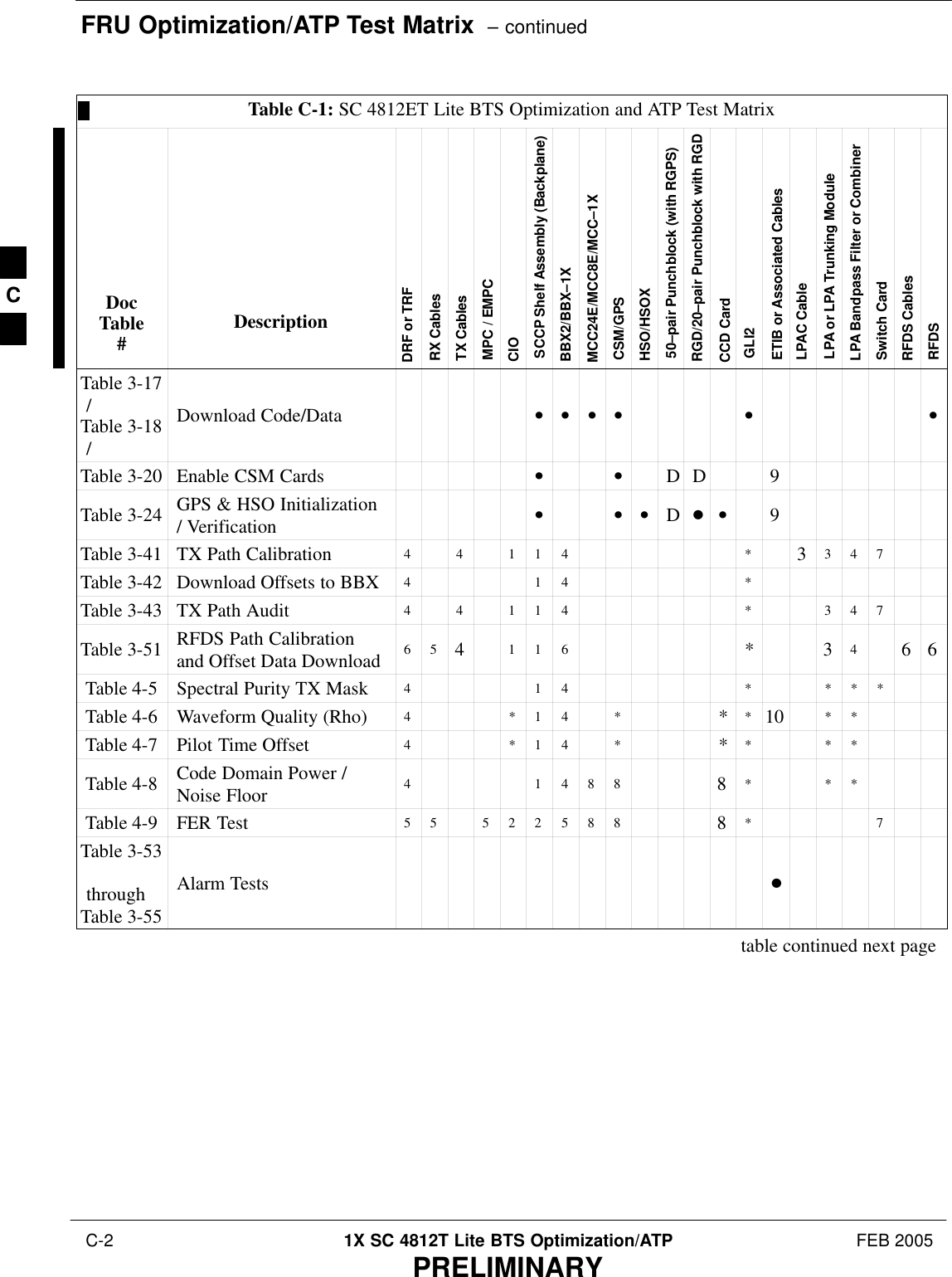
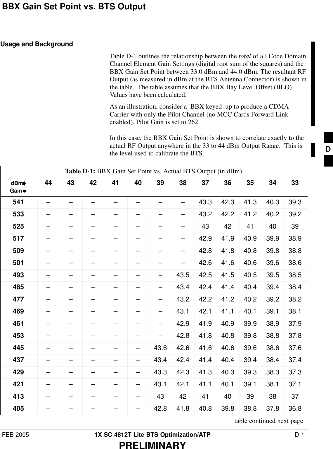
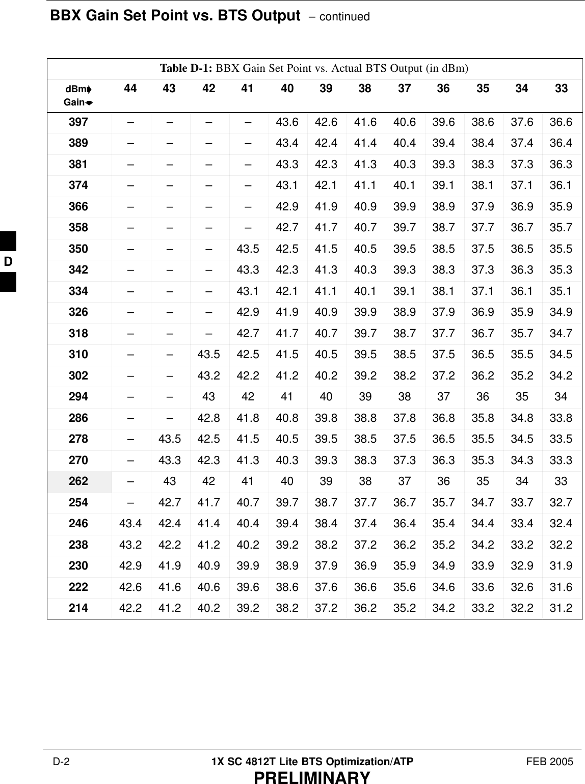
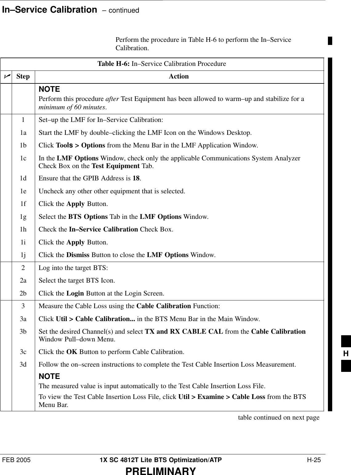
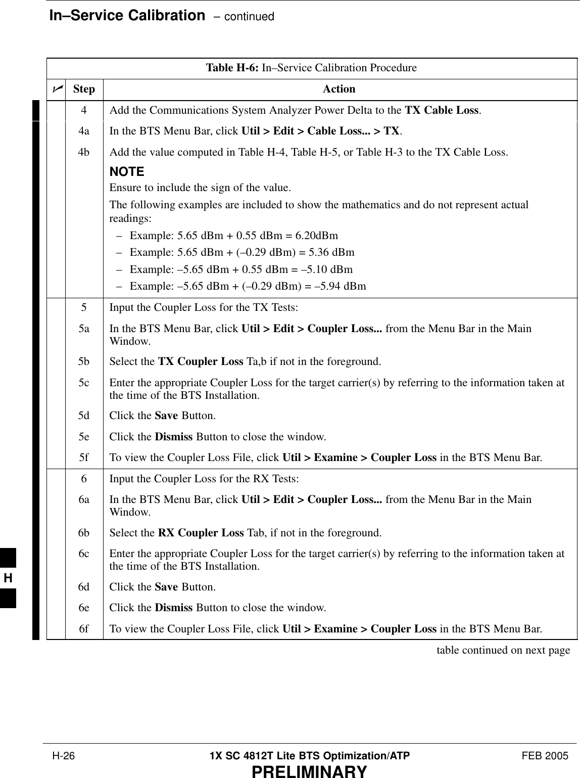
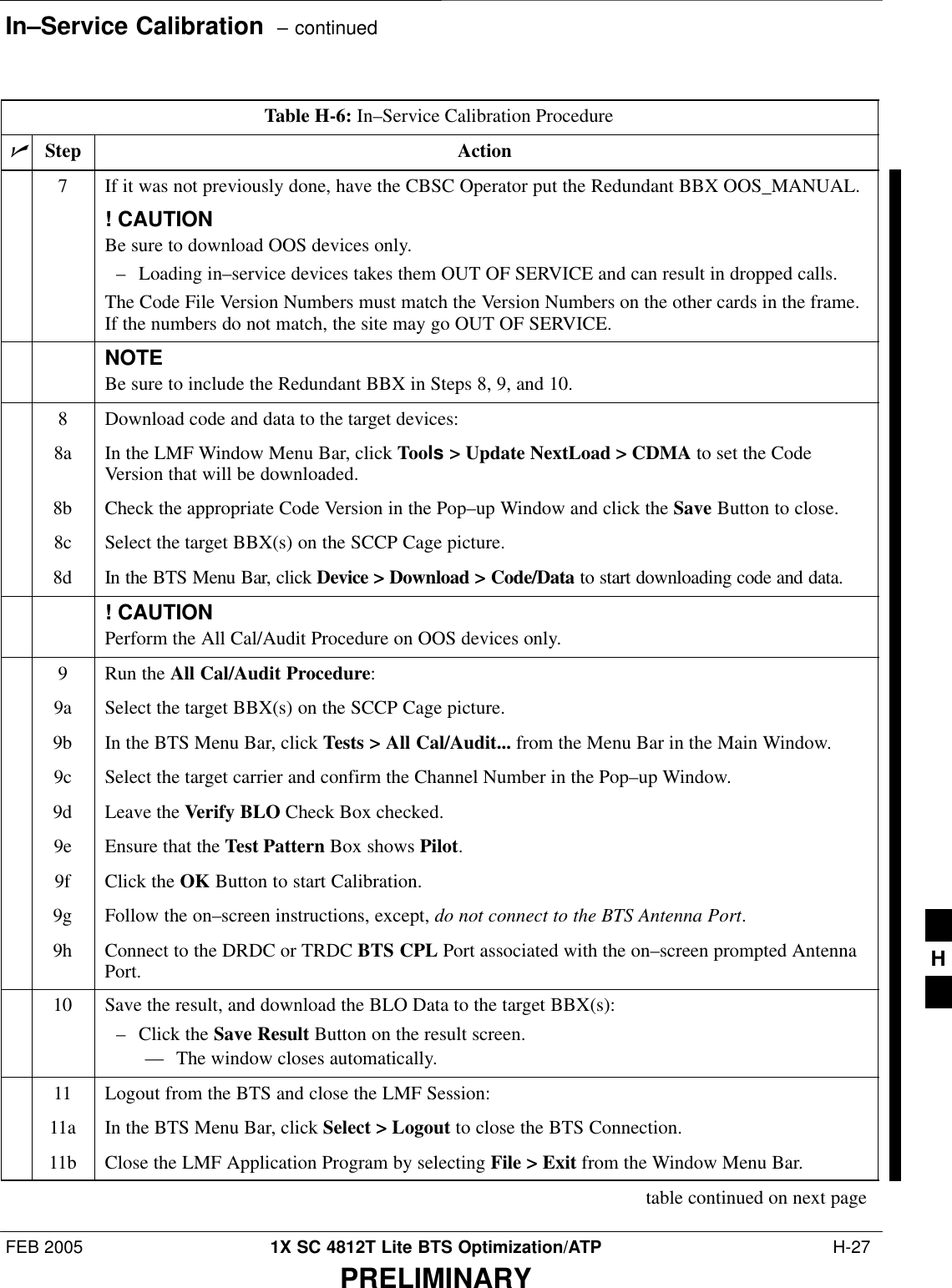
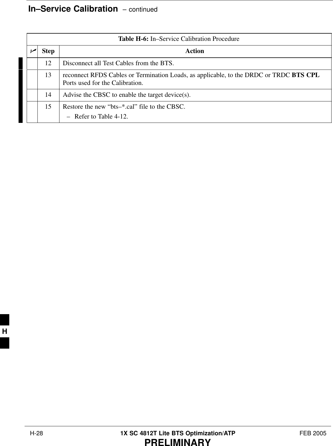
![TX Code Domain Power/Noise Floor Acceptance Test 4-20 1X SC 4812T Lite BTS Optimization/ATP FEB 2005PRELIMINARYBackgroundOverview This test verifies the Code Domain Power and Noise Floor of eachoperator–selected BBX Carrier keyed at a specific frequency specified inthe current CDF. All tests are performed using the external, calibratedTest Equipment controlled by the same command. All measurements aremade at the appropriate BTS TX Antenna Connector..CDMA Channel Test Set–up Pilot Gain should be set to 262 for each antenna and the selected MCCCards should be configured to supply all odd–numbered Walsh CodeTraffic Channel Elements by enabling Orthogonal Channel Noise Source(OCNS) on all odd MCC Channel Elements (maximum 32 Full RateChannels with an OCNS Gain of 81). – All even–numbered Walsh Code Traffic Channel Elements shouldhave OCNS disabled, and are considered “OFF”. – Selected MCC Cards should be Forward–Link Enabled for theantenna (sector) under test..Equipment Operation During Testing The BBX should be keyed–up using a BLO–corrected bbxlvl Value togenerate a CDMA Carrier consisting of Pilot and OCNS Channels. RFOutput Power, as measured at the appropriate Frame TX AntennaConnector, is set at one of the following values depending on theOperating Frequency Spectrum.:– 800 MHz: 33.5 dBm– 1.9 GHz: 31.0 dBmTest Measurements The Test Equipment will measure and return the Channel ElementPower in dB of all specified Walsh Channels within the CDMAspectrum. Additional calculations will be performed to verify that thefollowing parameters are met. – Refer to Figure 4-3 for graphic representations.:STraffic Channel Element Power Level will be verified by calculatingthe ratio of Pilot Power to OCNS Gain of all Traffic Channels [RootSum of the Square (RSS) of each OCNS Gain divided by the PilotPower].– This value should be 10.2 dB + 2.0 dB.SNoise Floor (unassigned “OFF” even–numbered Walsh Channels) isverified to be < –27 dB for IS–95A/B and CDMA2000 1X withrespect to total CDMA Channel Power.4](https://usermanual.wiki/Nokia-Solutions-and-Networks/T6FE1.User-Manual-3-of-3/User-Guide-520639-Page-22.png)


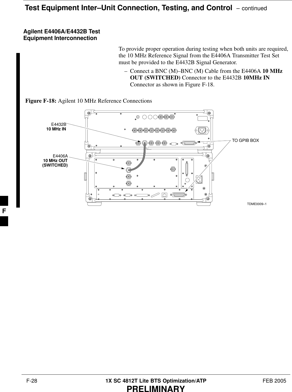
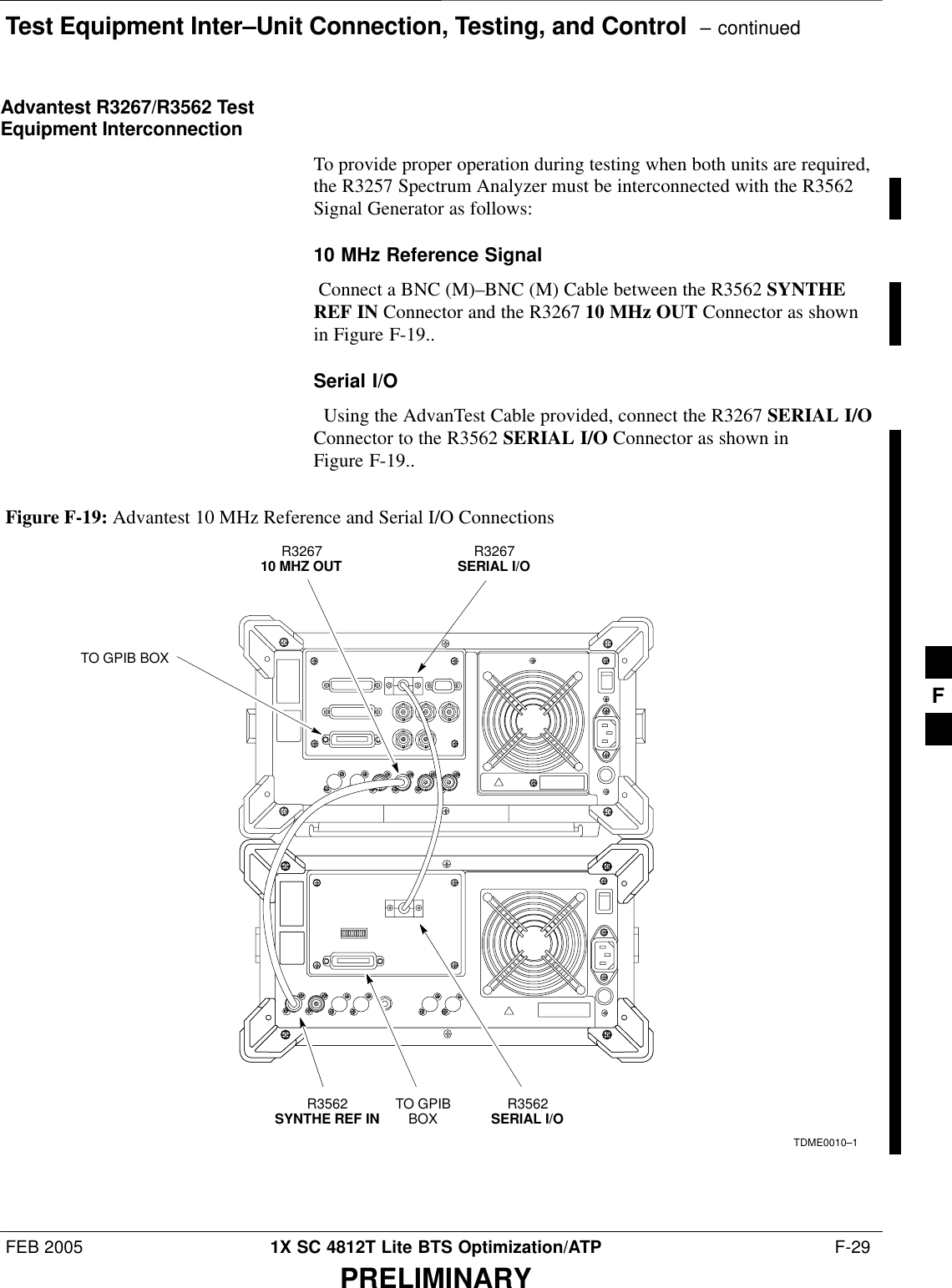
![Test Equipment Inter–Unit Connection, Testing, and Control – continued F-22 1X SC 4812T Lite BTS Optimization/ATP FEB 2005PRELIMINARYHP 8921A with PCS InterfaceSystem Connectivity TestPerform the procedure in Table F-15 to verify that the connectionsbetween the PCS Interface and the HP 8921A are correct and cables areintact. The software also performs basic functionality checks of eachinstrument.Disconnect other GPIB Devices, especially systemcontrollers, from the system before running theconnectivity software.NOTETable F-15: System Connectivity Test ProcedurenStep ActionNOTEPerform this procedure only after Test Equipment has been allowed to warm–up and stabilize for aminimum of 60 minutes.1Insert the HP 83236A Manual Control/System Card into the Memory Card Slot.2Press the [PRESET] Pushbutton.3Press the Screen Control [TESTS] Pushbutton to display the “Tests” Main Menu Screen.4Position the cursor on Select Procedure Location and select it by pressing the Cursor ControlKnob.5In the Choices Selection Box, select Card.6Position the cursor on Select Procedure Filename and select it by pressing the Cursor ControlKnob.7In the Choices Selection Box, select SYS_CONN.8Position the cursor on RUN TEST and select it.– The software will provide operator prompts through completion of the Connectivity Set–up.9Perform the following action when the test is complete.– Position cursor on STOP TEST and select it.OR– Press the [K5] Pushbutton.10 To return to the Main Menu, press the [K5] Pushbutton.11 Press the [PRESET] Pushbutton. F](https://usermanual.wiki/Nokia-Solutions-and-Networks/T6FE1.User-Manual-3-of-3/User-Guide-520639-Page-160.png)
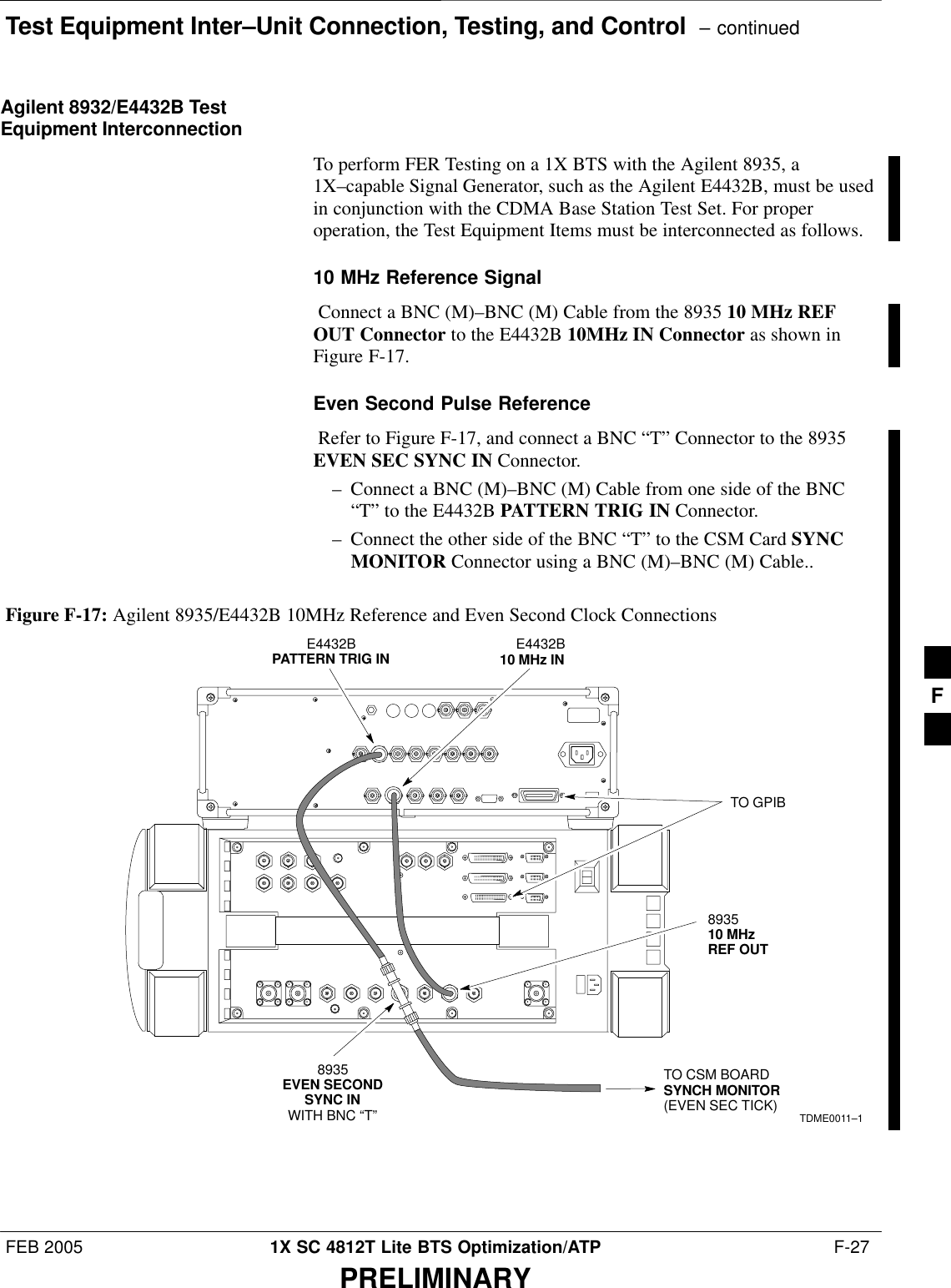
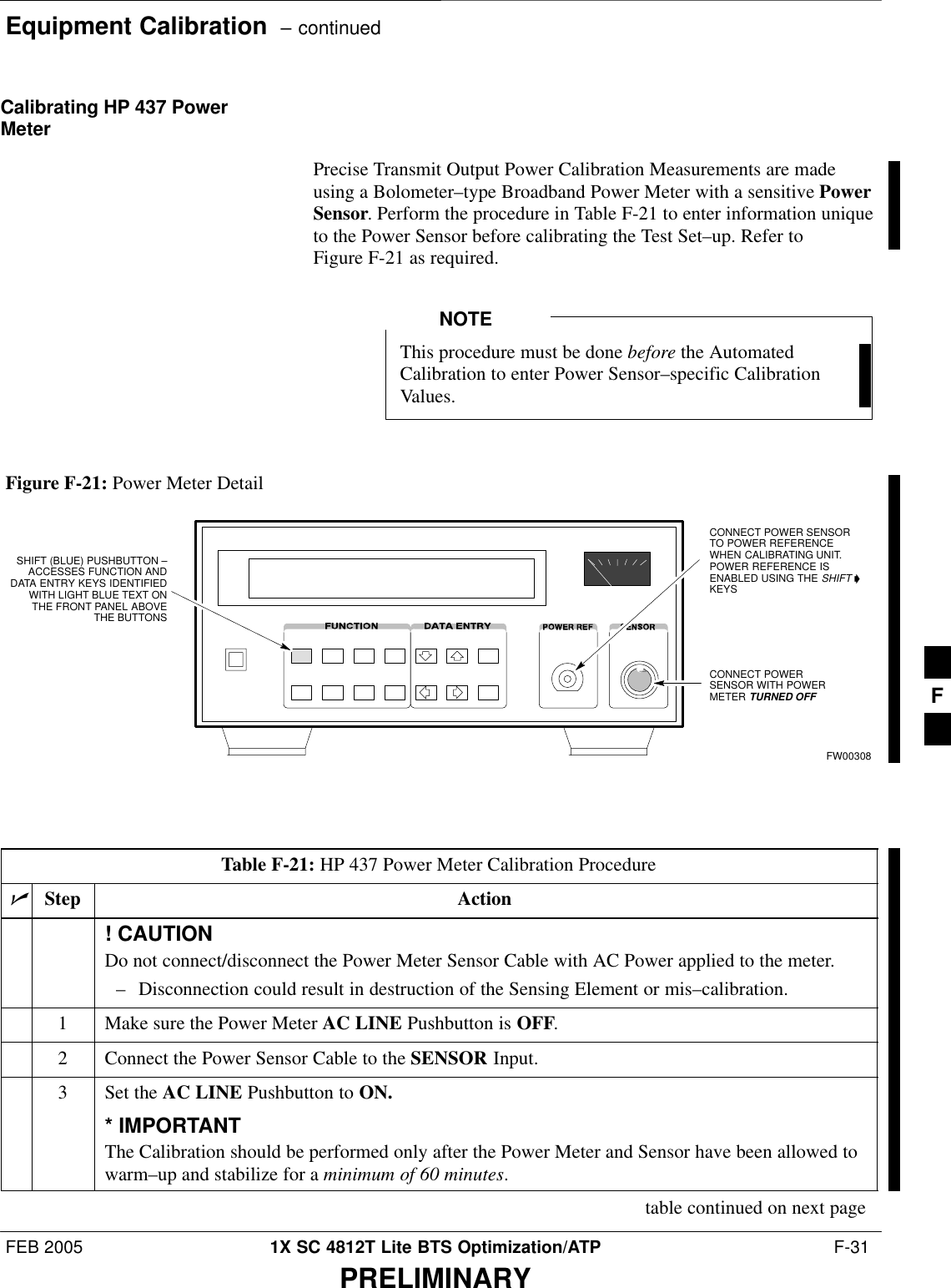
![Equipment Calibration – continued F-32 1X SC 4812T Lite BTS Optimization/ATP FEB 2005PRELIMINARYTable F-21: HP 437 Power Meter Calibration ProcedurenActionStep4Perform the following actions to set or verify that the correct Power Sensor Model:4a Press [SHIFT] then [a] to select SENSOR.4b Identify the Power Sensor Model Number from the Sensor Label.4c Use the [y] or [b] Button to select the appropriate model; then press [ENTER].5Ensure that the Power Reference Output is OFF.– Refer to the illustration for Step 9.6Observe the instrument display to determine if the triangular indicator over PWR REF isdisplayed.SIf the triangular indicator is not displayed, proceed to Step 7.SIf the triangular indicator is displayed:–Proceed to Step 8.– Press [SHIFT] then [’] to turn it off.7 Press [ZERO].– The display will show “Zeroing ******.”– Wait for the process to complete.8Connect the Power Sensor to the POWER REF Output.9Turn on the PWR REF by performing the following actions.9a Press [SHIFT] then [’].9b Verify that the triangular indicator (below) appears in the display above PWR REF.10 Perform the following actions to set the REF CF%.10a Press ([SHIFT] then [ZERO]) for CAL.10b Enter the Sensor’s REF CF% from the Sensor’s Decal using the Arrow Keys and press [ENTER].– The Power Meter will display ”CAL *****” for a few seconds.NOTEIf the REF CAL FACTOR (REF CF) is not shown on the Power Sensor, assume it to be 100%.table continued on next pageF](https://usermanual.wiki/Nokia-Solutions-and-Networks/T6FE1.User-Manual-3-of-3/User-Guide-520639-Page-170.png)
![Equipment Calibration – continuedFEB 2005 1X SC 4812T Lite BTS Optimization/ATP F-33PRELIMINARYTable F-21: HP 437 Power Meter Calibration ProcedurenActionStep11 Perform the following actions to set the CAL FAC %:11a Press [SHIFT] then [FREQ] for CAL FAC.11b On the Sensor’s Decal, locate an approximate Calibration Percentage Factor (CF%) at 2 GHz.11c Enter the Sensor’s Calibration % (CF%) using the Arrow Keys and press [ENTER].– When complete, the Power Meter will typically display 0.05 dBm; any reading between 0.00and 0.10 is normal.12 To turn off the PWR REF, perform the following actions.12a Press [SHIFT] then [’].12b Disconnect the Power Sensor from the POWER REF Output. F](https://usermanual.wiki/Nokia-Solutions-and-Networks/T6FE1.User-Manual-3-of-3/User-Guide-520639-Page-171.png)
![Manual Cable Calibration – continued F-36 1X SC 4812T Lite BTS Optimization/ATP FEB 2005PRELIMINARYTable F-23: Test Cable Set–up (using the HP PCS Interface) Calibration ProcedurenActionStep9Set the Channel Number=<chan#> by performing the following actions.9a Position the cursor on Channel Number and select it.9b Enter the chan# using the Numeric Keypad.9c Press [Enter].– The screen will go blank.– When the screen reappears, the chan# will be displayed on the Channel Number Line.9d Proceed to Step 11.10 Set the Channel Frequency by performing the following actions.10a Position the cursor on Frequency Band and press Enter.10b Select User Defined Frequency.10c Go Back to Previous Menu.10d Position the cursor to 83236 Generator Frequency and enter actual RX Frequency.10e Position the cursor to 83236 Analyzer Frequency and enter actual TX Frequency.11 Set the RF Generator Level by performing the following actions.11a Position the cursor on RF Generator Level and select it.11b Enter –10 using the Numeric Keypad.11c Press [Enter].– The screen will go blank.– When the screen reappears, the value –10 dBm will be displayed on the RF Generator LevelLine.12 Set the user–fixed Attenuation Setting to 0 dBm by performing the following actions.12a Position the cursor on Analyzer Attenuation and select it12b Position the cursor on User Fixed Atten Settings and select it.12c Enter 0 (zero) using the Numeric Keypad and press [Enter].13 Select Back to Previous Menu.14 Record the Generator Frequency Level .SIf using the HP83226A, proceed to Step 15.SIf using the HP83226B, proceed to Step 16.table continued on next pageF](https://usermanual.wiki/Nokia-Solutions-and-Networks/T6FE1.User-Manual-3-of-3/User-Guide-520639-Page-174.png)
![Manual Cable Calibration – continued F-38 1X SC 4812T Lite BTS Optimization/ATP FEB 2005PRELIMINARYTable F-23: Test Cable Set–up (using the HP PCS Interface) Calibration ProcedurenActionStep25 Calculate the Total Test Set–up Loss Value by adding up all the individual Loss Values:SExample: Total Test Set–up Loss Value = –1.4 –29.8 –20.1 = –51.3 dB.– This calculated value will be used in the next series of tests.26 Under Screen Controls press the TESTS Button to display the TESTS (Main Menu) Screen.27 Select Continue (K2).28 Select RF Generator Level and set to –119 dBm.29 Click on Pause for Manual Measurement.30 Verify the GPIB (HP–IB) Address (HP 8921A Communication Analyzer/83203A CDMAInterface).– Fields not specifically identified remain at default values.30a Under To Screen, select More.30b Select IO CONFIG.30c Set HP–IB Adrs to 18.30d Set Mode to Talk&Lstn.31 Verify that the HP 8921A is displaying Frequency instead of RF Channel.31a Press the blue [SHIFT] Button, then press the Screen Control [DUPLEX] Button; this switches tothe CONFIG (CONFIGURE) Screen.31b Use the Cursor Control to set RF Display to Freq.32 Refer to Chapter 3 for assistance in setting the Test Cable Insertion Loss Values into the LMF. F](https://usermanual.wiki/Nokia-Solutions-and-Networks/T6FE1.User-Manual-3-of-3/User-Guide-520639-Page-176.png)
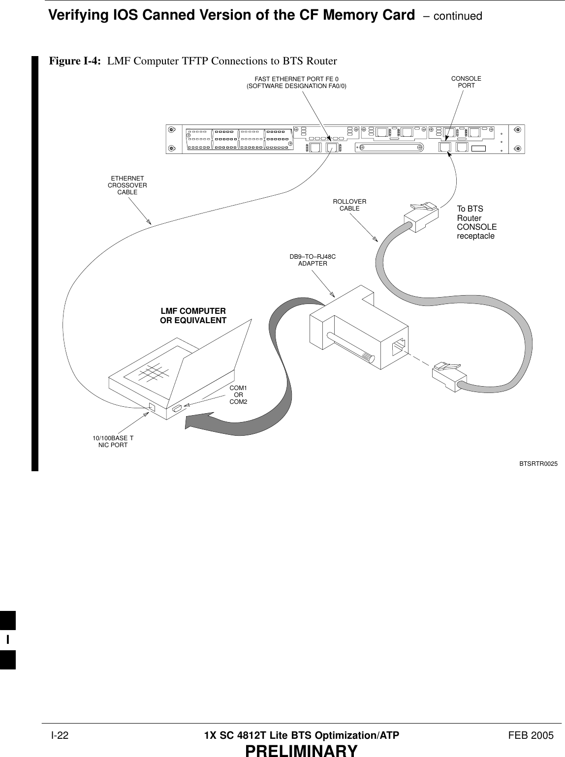
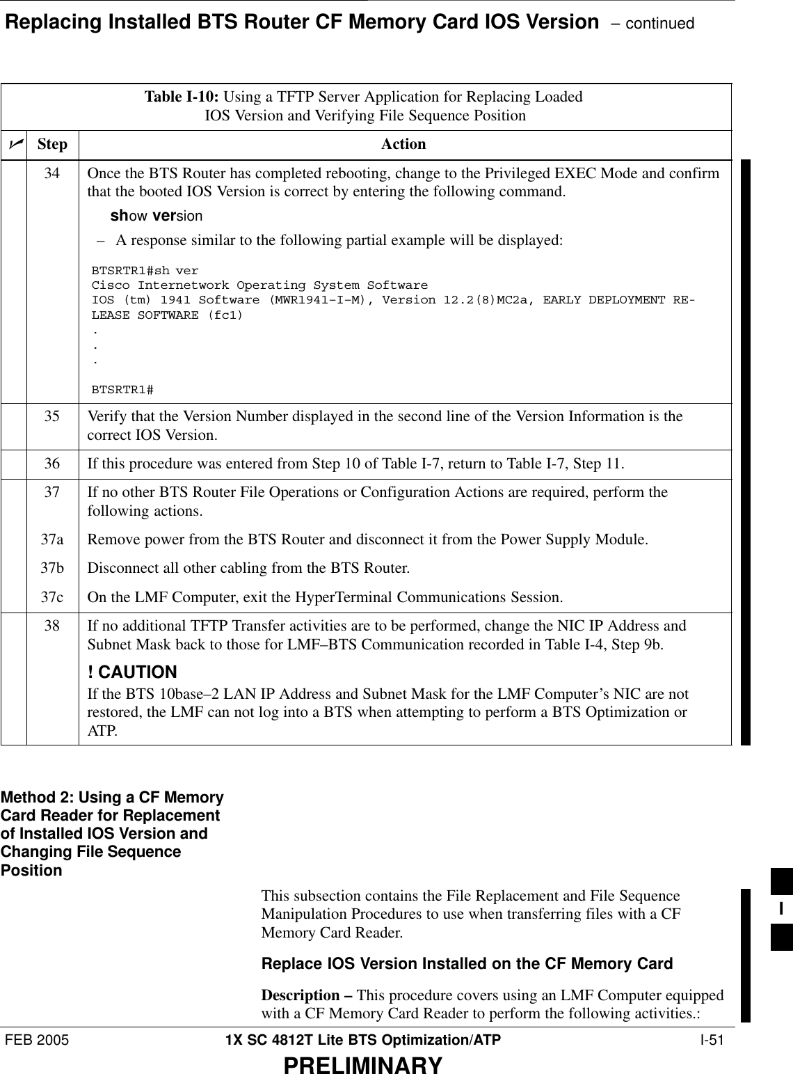
![Verifying IOS Canned Version of the CF Memory Card – continuedFEB 2005 1X SC 4812T Lite BTS Optimization/ATP I-23PRELIMINARYBTS Router Power–up and Initial Configuration for EthernetCommunicationPerform the procedure in Table I-6 to apply power to the BTS Routerand set an Initial Configuration for Ethernet Communication.SEnsure that the required version of the IOS is loaded on the CFMemory Card.SEnsure that the CF Memory Card is installed in the BTS Router.Table I-6: BTS Router Power–up and Initial Ethernet Configuration ProcedurenStep Action* IMPORTANTThis procedure does not cover all aspects of BTS Router Operation and programming.Before performing this procedure, review BTS Router initialization, operation, and programminginformation and procedures in MWR1941 Wireless Mobile Edge Router Software ConfigurationGuide; part number 78–13983–01.– Have this publication available for reference while performing this procedure.1Ensure that a CF Memory Card loaded with the Cisco IOS is installed in the BTS Router.– Refer to the BTS Router Card and Module Replacement section of the 1X SC4812T Lite BTSFRU manual (68P09262A60) for instructions to access the CF Memory Card Slot.* IMPORTANTIn Step 2, do not touch the computer keyboard until the BTS Router completes the Boot Process.The BTS Router buffers any keystrokes made during the Boot Process and interprets them ascommands to be executed immediately following completion of the Boot Process.2Apply power to the BTS Router and allow it to complete the Boot Process.SIf a message similar to the following, is displayed, press the Enter Key and proceed to Step 3.Press RETURN to get started!SIf a message similar to the following, is displayed type no and press the Enter Key:Basic management set–up configures only enough connectivityfor management of the system, extended set–up will ask youto configure each interface on the systemWould you like to enter basic management set–up? [yes/no]:A response similar to the following will be displayed:Would you like to enter basic management set–up? [yes/no]: noCisco Internetwork Operating System SoftwareIOS (tm) 1941 Software (MWR1941–I–M), Version 12.2(20020127:101239Copyright (c) 1986–2002 by cisco Systems, Inc.Compiled Sun 27–Jan–02 06:08 by walrobinRouter>table continued on next pageI](https://usermanual.wiki/Nokia-Solutions-and-Networks/T6FE1.User-Manual-3-of-3/User-Guide-520639-Page-241.png)
![Verifying IOS Canned Version of the CF Memory Card – continued I-28 1X SC 4812T Lite BTS Optimization/ATP FEB 2005PRELIMINARYTable I-7: Transfer Canned Configuration Files to the BTS Router Using a TFTP ServernActionStep8Direct the BTS Router to show the Version Information by entering the following command.show version– A response similar to the following will be displayed:BTSRTR1#sh verCisco Internetwork Operating System Software IOS (tm) 1941 Software (MWR1941–I–M), Version 12.2(8)MC2a, EARLY DEPLOYMENT RE-LEASE SOFTWARE (fc1)TAC Support: http://www.cisco.com/tacCopyright (c) 1986–2002 by cisco Systems, Inc.Compiled Mon 05–Aug–02 11:07 by nmasaImage text–base: 0x60008940, data–base: 0x60B54000ROM: System Bootstrap, Version 12.2(20020113:235343) [sbose–wilma 109], DEVELOP-MENT SOFTWAREROM: 1941 Software (MWR1941–I–M), Version 12.2(8)MC2a, EARLY DEPLOYMENT RELEASESOFTWARE (fc1)Router uptime is 1 minuteSystem returned to ROM by power–onSystem image file is ”slot0:mwr1941–i–mz.122–8.MC2a.bin”cisco mwr1941 (R7000) processor (revision 0.1) with 121856K/18432K bytes ofmemory.Processor board ID JMX0611K5TSR7000 CPU at 240Mhz, Implementation 39, Rev 3.3, 256KB L2 CacheBridging software.X.25 software, Version 3.0.0.Primary Rate ISDN software, Version 1.1.Toaster processor tmc is running.2 FastEthernet/IEEE 802.3 interface(s)2 Serial network interface(s)2 Channelized T1/PRI port(s)DRAM configuration is 64 bits wide with parity disabled.55K bytes of non–volatile configuration memory.31360K bytes of ATA Slot0 CompactFlash (Read/Write)Configuration register is 0x101BTSRTR1#9Compare the IOS Filename returned in Step 5 and the second line of the Version Information inStep 8.– Note the correspondence between the filename and IOS Version information.SIf the IOS Filename from the CF Memory Card returned in Step 5 is not different than thefilename of the required IOS Version loaded in the LMF Computer Default TFTP Directory,proceed to Step 11.SIf the IOS Filename from the CF Memory Card returned in Step 5 is different than the filenameof the required IOS Version loaded in the LMF Computer Default TFTP Directory, proceed toStep 10.10 Perform the procedure in Table I-13 to load the required version, then proceed to Step 11.table continued on next pageI](https://usermanual.wiki/Nokia-Solutions-and-Networks/T6FE1.User-Manual-3-of-3/User-Guide-520639-Page-246.png)
![Verifying IOS Canned Version of the CF Memory Card – continuedFEB 2005 1X SC 4812T Lite BTS Optimization/ATP I-29PRELIMINARYTable I-7: Transfer Canned Configuration Files to the BTS Router Using a TFTP ServernActionStep! CAUTIONThe File Sequence on the CF Memory Card can not be verified with Application Programs thatplace the listed file names in alphabetical order (for example, certain UNIX Telnet Applications,UNIX Directory Listing Commands, and Windows File Managers such as Windows Explorer).This portion of the procedure is intended for use only with applications, such as HyperTerminal,that do not list directory contents alphabetically.11 Verify that the IOS Version is correct.SIf the IOS Version is correct and there is more than one file loaded on the CF Memory Card,ensure that the IOS File is the first file listed in the Directory Content Display.SIf it is not correct, proceed to Step 12.12 Prepare the LMF for the correct IOS Version.12a Backup all files on the CF Memory Card to the LMF Computer Default TFTP Directory byperforming Step 3 through Step 6 of Table I-13.12b Perform Step 25 through Step 30 of Table I-13, as applicable.12c Type the following to delete a possible Boot System Line in the startup–config File, pressingthe Enter Key after the command and at each prompt to confirm the filename and deletionoperation.del nvram:startup–config– A response similar to the following will be displayed:BTSRTR1#del nvram:startup–configDelete filename [startup–config]? Delete nvram:startup–config? [confirm][OK]BTSRTR1#NOTEEnsure to include the colon (:) after nvram when typing the command.12d Verify that the startup–config File size has been reduced to a minimum by entering thefollowing command.dir nvram:– A response similar to the following will be displayed:Router#dir nvram:Directory of nvram:/ 53 –rw– 5 <no date> startup–config 54 –––– 5 <no date> private–config57336 bytes total (57274 bytes free)BTSRTR1#table continued on next pageI](https://usermanual.wiki/Nokia-Solutions-and-Networks/T6FE1.User-Manual-3-of-3/User-Guide-520639-Page-247.png)
![Verifying IOS Canned Version of the CF Memory Card – continued I-30 1X SC 4812T Lite BTS Optimization/ATP FEB 2005PRELIMINARYTable I-7: Transfer Canned Configuration Files to the BTS Router Using a TFTP ServernActionStep13 At the Privileged EXEC Mode Prompt, enter the following command.copy TFTP:btsrtr_canned.color slot0:canned–config– Where color = blue or red, as applicable.– A response similar to the following will be displayed:BTSRTR1#copy TFTP:btsrtr_canned.blue slot0:canned–configAddress or name of remote host []?14 At the prompt for the Remote Host Address or Name, enter the IP Address of the LMF ComputerNIC:100.100.100.1– A response similar to the following will be displayed:BTSRTR1#copy TFTP:btsrtr_canned.blue slot0:canned–configAddress or name of remote host []? 100.100.100.1Destination filename [canned–config]?15 At the prompt for the Destination Filename, press the Enter Key.– A response similar to the following will be displayed:BTSRTR1#copy TFTP:btsrtr_canned.blue slot0:canned–configAddress or name of remote host []? 100.100.100.1Destination filename [canned–config]?Loading btsrtr_canned.blue from 100.100.100.1 (via Ethernet0/0): ![OK – 2457/4096 bytes]2457 bytes copied in 84.724 secs (29 bytes/sec)BTSRTR1#16 Verify that the Canned Configuration File is saved on the CF Memory Card by entering the dirCommand.– A response similar to the following will be displayed:Directory of slot0:/ 1 –rw– 7051976 Mar 01 1993 00:11:34 mwr1941–i–mz.122–8.MC2a.bin 2 –rw– 2457 Mar 01 1993 00:14:48 canned–config31932416 bytes total (24877983 bytes free)BTSRTR1#17 To allow the BTS Router to boot using the Canned Configuration, enter the following command.copy canned–config startup–config– A response similar to the following will be displayed:BTSRTR1#copy canned–config startDestination filename [startup–config]?table continued on next pageI](https://usermanual.wiki/Nokia-Solutions-and-Networks/T6FE1.User-Manual-3-of-3/User-Guide-520639-Page-248.png)
![Verifying IOS Canned Version of the CF Memory Card – continuedFEB 2005 1X SC 4812T Lite BTS Optimization/ATP I-31PRELIMINARYTable I-7: Transfer Canned Configuration Files to the BTS Router Using a TFTP ServernActionStep18 When prompted for the Destination File Name, press the Enter Key.– A response similar to the following will be displayed:BTSRTR1#copy canned–config startDestination filename [startup–config]?2457 bytes copied in 3.52 secsBTSRTR1#19 Display and note the file size of the startup–config File by entering the following command.dir nvram:– A response similar to the following will be displayed:Directory of nvram:/ 26 –rw– 2457 <no date> startup–config 27 –––– 5 <no date> private–config29688 bytes total (24774 bytes free)BTSRTR1#20 Scroll the HyperTerminal Window back to the slot0: Directory Display obtained in Step 16,above.21 Compare the file size of the startup–config File to the Canned Configuration File to verify theCopy Operation.– The file sizes should be the same.22 If desired, the contents of the startup–config File may be verified against the file listings atthe end of this appendix for the blue or red Canned Configuration, as applicable, by entering thefollowing command.show startup–configNOTEPressing the Space Bar at the MORE prompt will scroll another full screen of data.Pressing the Enter Key will scroll the screen one line at a time.23 Verify that the BTS Router will boot properly on the IOS and revised Start–upConfiguration Files by entering the following command.reload– A response similar to the following will be displayed:BTSRTR1#reloadSystem configuration has been modified. Save? [yes/no]: nProceed with reload? [confirm]24 If prompted to save a modified configuration, enter n for “no,” and press the Enter Key.25 When prompted to proceed with Reload, press the Enter Key to continue the Reload Operation.table continued on next pageI](https://usermanual.wiki/Nokia-Solutions-and-Networks/T6FE1.User-Manual-3-of-3/User-Guide-520639-Page-249.png)
![Verifying IOS Canned Version of the CF Memory Card – continued I-32 1X SC 4812T Lite BTS Optimization/ATP FEB 2005PRELIMINARYTable I-7: Transfer Canned Configuration Files to the BTS Router Using a TFTP ServernActionStep26 Verify that the BTS Router reboots without displaying the rommon 1 > Prompt or Error Messagesrelated to Port Configurations.SIf the BTS Router boots to the ROMMON Prompt, proceed to the Recovery from BTS RouterBoot to ROMMON section of this appendix.27 Using the tagging materials, tag the BTS Router to clearly identify the installed configuration[blue (BTSRTR1) or red (BTSRTR2)].28 Remove the CF Memory from the BTS Router by performing the procedure in the 1X SC4812TLite BTS FRU manual (68P09262A60) Manual.29 Mark the installed configuration (blue or red) on the Card Label.30 Install the card in the BTS Router by performing the procedure in the 1X SC4812T Lite BTS FRUmanual (68P09262A60)31 If an additional BTS Router needs have the Canned Configuration installed, perform the followingactions.31a Disconnect the cabling from the BTS Router.31b Remove power from the BTS Router and disconnect it from the Power Supply Module.31c Repeat the procedures in Table I-5, Table I-6, and this table (Table I-7) using the additional BTSRouter.32 If no additional BTS Routers must be configured, perform Steps 31a and 31b, then proceed toStep 33.33 On the LMF Computer, shut down the TFTP Server Application and exit the HyperTerminalSession.34 If no additional TFTP Transfer activities are to be performed, change the NIC IP Address andSubnet Mask back to those for LMF–BTS Communication recorded in Table I-4, Step 9b.! CAUTIONIf the BTS 10base–2 LAN IP Address and Subnet Mask for the LMF Computer’s NIC are notrestored, the LMF can not log into a BTS when attempting to perform a BTS Optimization orATP. I](https://usermanual.wiki/Nokia-Solutions-and-Networks/T6FE1.User-Manual-3-of-3/User-Guide-520639-Page-250.png)
![Verifying IOS Canned Version of the CF Memory Card – continuedFEB 2005 1X SC 4812T Lite BTS Optimization/ATP I-35PRELIMINARYTransfer the Canned Configuration Files from the LMF Computer to aBTS Router CF Memory Card by performing the procedure in Table I-8.Table I-8: Transfer Canned Configuration File to CF Memory Card with CF Memory Card ReadernStep Action* IMPORTANTThis procedure does not cover all aspects of BTS Router Operation and programming.Before performing this procedure, review BTS Router initialization, operation, and programminginformation and procedures in MWR1941 Wireless Mobile Edge Router Software ConfigurationGuide; part number 78–13983–01.– Have this publication available for reference while performing this procedure.1If it has not been done, install a CF Memory Card loaded with the IOS in the BTS Router byperforming the procedure in the 1X SC4812T Lite BTS FRU manual (68P09262A60).* IMPORTANTMWR 1941 Routers must be loaded with IOS Version mwr1900–i–mz.122–8.MC2d.bin or later.This Router model will not function properly with earlier IOS Versions.2Connect the LMF Computer to the BTS Router and start a HyperTerminal CommunicationSession with the BTS Router by performing the procedure in Table I-2.3If it has not been done, connect the BTS Router to the +27V DC Power Supply Module.– Make sure that the +27V DC Power Supply Module Output is OFF.* IMPORTANTIn Step 4, do not touch the computer keyboard until the BTS Router completes the Boot Process.The BTS Router buffers any keystrokes made during the Boot Process and interprets them ascommands to be executed immediately following Boot Process completion.4Apply power to the BTS Router and allow it to complete the Boot Process.SIf a message similar to the following, is displayed, press the Enter Key and proceed to Step 5:Press RETURN to get started!5If a message similar to the following, is displayed type no and press the Enter Key:Basic management set–up configures only enough connectivityfor management of the system, extended set–up will ask youto configure each interface on the systemWould you like to enter basic management set–up? [yes/no]:A response similar to the following will be displayed:Would you like to enter basic management set–up? [yes/no]: noCisco Internetwork Operating System SoftwareIOS (tm) 1941 Software (MWR1941–I–M), Version 12.2(20020127:101239Copyright (c) 1986–2002 by cisco Systems, Inc.Compiled Sun 27–Jan–02 06:08 by walrobinRouter>table continued on next pageI](https://usermanual.wiki/Nokia-Solutions-and-Networks/T6FE1.User-Manual-3-of-3/User-Guide-520639-Page-253.png)
![Verifying IOS Canned Version of the CF Memory Card – continuedFEB 2005 1X SC 4812T Lite BTS Optimization/ATP I-39PRELIMINARYTable I-9: Copy Canned Configuration File to BTS Router Start–up Configuration and Verify IOS File PositionnActionStep4Display the Directory Listing of the CF Memory Card by entering the following command.dir– A response similar to the following will be displayed:Router#dir slot0:Directory of slot0:/ 1 –rw– 7051976 Sep 23 2002 07:24:18 mwr1941–i–mz.122–8.MC2a.bin 2 –rw– 2212 Mar 01 1993 00:14:48 canned–config31932416 bytes total (24885606 bytes free)Router#5Ensure that the IOS File is the first file listed in the Directory Content Display.SIf it is not, perform the procedure in Table I-12, and then return to Step 6, below.6Copy the Canned Configuration to the BTS Router’s Start–up Configuration File by entering thefollowing command.copy slot0:canned–config startup–config– A response similar to the following will be displayed:Router#copy slot0:canned–config startDestination filename [startup–config]?7When prompted for the Destination File Name, press the Enter Key.– A response similar to the following will be displayed:Router#copy slot0:canned–config startDestination filename [startup–config]?2218 bytes copied in 3.52 secsRouter1#8Check the file size of the startup–config File to verify the copy operation by entering thefollowing command.dir nvram:– A response similar to the following will be displayed:Directory of nvram:/ 26 –rw– 2218 <no date> startup–config 27 –––– 5 <no date> private–config29688 bytes total (25247 bytes free)Router#* IMPORTANTBe sure to include the colon (:) after nvram when typing the command.table continued on next pageI](https://usermanual.wiki/Nokia-Solutions-and-Networks/T6FE1.User-Manual-3-of-3/User-Guide-520639-Page-257.png)
![Verifying IOS Canned Version of the CF Memory Card – continued I-40 1X SC 4812T Lite BTS Optimization/ATP FEB 2005PRELIMINARYTable I-9: Copy Canned Configuration File to BTS Router Start–up Configuration and Verify IOS File PositionnActionStep9If desired, the contents of the startup–config File may be verified against the file listings atthe end of this appendix for the blue or red Canned Configuration, as applicable, by entering thefollowing command.show startup–configNOTEPressing the Space Bar at the MORE Prompt will scroll to another full screen of data.Pressing the Enter Key will scroll the screen one line at a time.10 Verify that the BTS Router will boot properly on the IOS and revised Start–up Configuration Filesby entering the following command.reload– A response similar to the following will be displayed:Router#reloadSystem configuration has been modified. Save? [yes/no]: nProceed with reload? [confirm]11 If prompted to save a modified configuration:– Enter n for “no”.– Press the Enter Key.12 When prompted to proceed with reload:– Press the Enter Key to continue the Reload Operation.13 Verify that the BTS Router reboots without displaying the rommon 1 > Prompt or Error Messagesrelated to Port Configurations.SIf the BTS Router does boot to the ROMMON Prompt, proceed to the Recovery from BTSRouter Boot to ROMMON section of this appendix.SIf the BTS Router does not boot to the ROMMON Prompt, proceed to Step 14.14 Using the tagging materials, tag the BTS Router to clearly identify the installed configuration[blue (BTSRTR1) or red (BTSRTR2)].15 Determine if additional BTS Routers need to be configured.SIf no additional BTS Routers need to be configured, perform Step 16, Step 17, and Step 19 only.–Do not perform Step 18.SIf any additional BTS Router need to be configured, perform Step 16, Step 17, Step 18, andStep 19.16 Disconnect the cabling for the HyperTerminal Communications Session from the BTS Router, andminimize the HyperTerminal Window on the LMF Computer.17 Remove power from the BTS Router and disconnect it from the Power Supply Module.table continued on next pageI](https://usermanual.wiki/Nokia-Solutions-and-Networks/T6FE1.User-Manual-3-of-3/User-Guide-520639-Page-258.png)
![Replacing Installed BTS Router CF Memory Card IOS Version – continued I-44 1X SC 4812T Lite BTS Optimization/ATP FEB 2005PRELIMINARYTable I-10: Using a TFTP Server Application for Replacing Loaded IOS Version and Verifying File Sequence PositionnStep Action* IMPORTANTThis procedure does not cover all aspects of BTS Router Operation and programming.Before performing this procedure, review BTS Router initialization, operation, and programminginformation and procedures in MWR1941 Wireless Mobile Edge Router Software ConfigurationGuide; part number 78–13983–01.– Have this publication available for reference while performing this procedure.1This procedure assumes the LMF Computer and BTS Router are configured, connected, andoperating as they would be after performing the procedures in Table I-4, Table I-5, Table I-6, andSteps 1 through 10 of Table I-7.– If necessary, perform these procedures now.NOTEThe present IOS Working Directory defaults to the CF Memory Card (slot0:) Directory unless thepresent Working Directory has been changed by using the cd Command.2Identify the present Working Directory by entering pwd.SIf the present Working Directory has been changed, enter the command cd slot0: to return tothe default setting.3Identify the filename of the currently loaded IOS that must be replaced by entering dir command.– A response similar to the following will be displayed:BTSRTR1#dirDirectory of slot0:/ 1 –rw– 7051844 Sep 23 2002 07:15:08 mwr1941–i–mz.07022002.bin 2 –rw– 2212 Mar 01 1993 00:11:00 canned–config31932416 bytes total (24878360 bytes free)BTSRTR1#4Begin to back–up the currently installed version of the BTS Router’s IOS to the LMF Computer’sDefault TFTP Directory by entering the following command.copy old_IOS_filename TFTP:– Where old_IOS_filename = the filename of the IOS currently loaded on the BTS Router CFMemory Card.– A response similar to the following will be displayed:BTSRTR1#copy mwr1941–i–mz.07022002.bin TFTP:Address or name of remote host []?table continued on next pageI](https://usermanual.wiki/Nokia-Solutions-and-Networks/T6FE1.User-Manual-3-of-3/User-Guide-520639-Page-262.png)
![Replacing Installed BTS Router CF Memory Card IOS Version – continuedFEB 2005 1X SC 4812T Lite BTS Optimization/ATP I-45PRELIMINARYTable I-10: Using a TFTP Server Application for Replacing Loaded IOS Version and Verifying File Sequence PositionnActionStep5At the Remote Host Prompt, enter the following:100.100.100.1– A response similar to the following will be displayed:Address or name of remote host []? 100.100.100.1Destination filename [mwr1941–i–mz.07022002.bin]?6If the Default Filename displayed in the prompt is correct, press the Enter Key to accept it.SIf it is missing or not correct, enter the correct filename.– A response similar to the following will be displayed if the Default Filename is selected:Address or name of remote host []? 100.100.100.1Destination filename [mwr1941–i–mz.07022002.bin]?!!!!!!!!!!!!!!!!!!!!!!!!!!!!!!!!!!!!!!!!!!!!!!!!!!!!!!!!!!!!!!!!!!!!!!!!!!!!!!!!!!!!!!!!!!!!!!!!!!!!!!!!!!!!!!!!!!!!!!!!!!!!!!!!!!!!!!!!!!!!!!!!!!!!!!!!!!!!!!!!!!!!!!!!!!!!!!!!!!!!!!!!!!!!!!!!!!!!!!!!!!!!!!!!!!!!!!!!!!!!!!!!!!!!!!!!!!!!!!!!!!!!!!!!!!!!!!!!!!!!!!!!!!!!!!!!!!!!!!!!!!!!!!!!!!!!!!!!!!!!!!!!!!!!!!!!!!!!!!!!!!!!!!!!!!!!!!!!!!!!!!!!!!!!!!!!!!!!!!!!!!!!!!!!!!!!!!!!!!!!!!!!!!!!!!!!!!!!!!!!!!!!!!!!!!!!!!!!!!!!!!!!!!!!!!!!!!!!!!!!!!!!!!!!!!!!!!!!!!!!!!!!!!!!!!!!!!!!!!!!!!!!!!!!!!!!!!!!!!!!!!!!!!!!!!!!!!!!!!!!!!!!!!!!!!!!!!!!!!!!!!!!!!!!!!!!!!!!!!!!!!!!!!!!!!!!!!!!!!!!!!!!!!!!!!!!!!!!!!!!!!!!!!!!!!!!!!!!!!!!!!!!!!!!!!!!!!!!!!!!!!!!!!!!!!!!!!!!!!!!!!!!!!!!!!!!!!!!!!!!!!!!!!!!!!!!!!!!!!!!!!!!!!!!!!!!!!!!!!!!!!!!!!!!!!!!!!!!!!!!!!!!!!!!!!!!!!!!!!!!!!!!!!!!!!!!!!!!!!!!!!!!!!!!!!!!!!!!!!!!!!!!!!!!!!!!!!!!!!!!!!!!!!!!!!!!!!!!!!!!!!!!!!!!!!!!!!!!!!!!!!!!!!!!!!!!!!!!!!!!!!!!!!!!!!!!!!!!!!!!!!!!!!!!!!!!!!!!!!!!!!!!!!!!!!!!!!!!!!!!!!!!!!!!!!!!!!!!!!!!!!!!!!!!!!!!!!!!!!!!!!!!!!!!!!!!!!!!!!!!!!!!!!!!!!!!!!!!!!!!!!!!!!!!!!!!!!!!!!!!!!!!!!!!!!!!!!!!!!!!!!!!!!!!!!!!!!!!!!!!!!!!!!!!!!!!!!!!!!!!!!!!!!!!!!!!!!!!!!!!!!!!!!!!!!!!!!!!!!!!!!!!!!!!!!!!!!!!!!!!!!!!!!!!!!!!!!!!!!!!!!!!!!!!!!!!!!!!!!!!!!!!!!!!!!!!!!!!!!!!!!!!!!!!!!!!!!!!!!!!!!!!!!!!!!!!!!!!!!!!!!!!!!!!!!!!!!!!!!!!!!!!!!!!!!!!!!!!!!!!!!!!!!!!!!!!!!!!!!!!!!!!!!!!!!!!!!!!!!!!!!!!!!!!!!!!!!!!!!!!!!!!!!!!!!!!!!!!!!!7051844 bytes copied in 109.92 secs (64697 bytes/sec)BTSRTR1#7If additional files are stored on the CF Memory Card, begin backing them up to the LMFComputer’s Default TFTP Directory by entering the following command.copy additional_filename TFTP:– Where additional_filename = the filename of an additional file loaded on the BTS RouterCF Memory Card.– A response similar to the following will be displayed:BTSRTR1#copy canned–config TFTP:Address or name of remote host [100.100.100.1]?8If the Default IP Address displayed in the prompt is correct, press the Enter Key to accept it.SIf it is missing or not correct, enter the correct IP Address for the LMF Computer.– A response similar to the following will be displayed if the Default Filename is selected:Address or name of remote host [100.100.100.1]? Source filename [canned–config]?table continued on next pageI](https://usermanual.wiki/Nokia-Solutions-and-Networks/T6FE1.User-Manual-3-of-3/User-Guide-520639-Page-263.png)
![Replacing Installed BTS Router CF Memory Card IOS Version – continued I-46 1X SC 4812T Lite BTS Optimization/ATP FEB 2005PRELIMINARYTable I-10: Using a TFTP Server Application for Replacing Loaded IOS Version and Verifying File Sequence PositionnActionStep9If the Default Filename displayed in the prompt is correct, press the Enter Key to accept it.SIf it is missing or not correct, enter the correct filename.– A response similar to the following will be displayed if the Default Filename is selected:Source filename [canned–config]? Destination filename [canned–config]?10 If the Default Filename displayed in the prompt is correct, press the Enter Key to accept it.SIf it is missing or not correct, enter the correct filename.– A response similar to the following will be displayed:Destination filename [canned–config]?![OK – 2212/4096 bytes]2212 bytes copied in 0.152 secsBTSRTR1#11 If more files are stored on the CF Memory Card, repeat Steps 7 through 10 until all files have beenbacked up to the LMF Computer.12 Delete all files from the CF Memory Card by entering the following command:format slot0:– A response similar to the following will be displayed:BTSRTR1#format slot0:Format operation may take a while. Continue? [confirm]13 Press the Enter Key to continue the Format Operation.– A response similar to the following will be displayed:Format operation may take a while. Continue? [confirm]Format operation will destroy all data in ”slot0:”. Continue? [confirm]table continued on next pageI](https://usermanual.wiki/Nokia-Solutions-and-Networks/T6FE1.User-Manual-3-of-3/User-Guide-520639-Page-264.png)
![Replacing Installed BTS Router CF Memory Card IOS Version – continuedFEB 2005 1X SC 4812T Lite BTS Optimization/ATP I-47PRELIMINARYTable I-10: Using a TFTP Server Application for Replacing Loaded IOS Version and Verifying File Sequence PositionnActionStep14 Press the Enter Key to continue the Format Operation.– A response similar to the following will be displayed:Format operation will destroy all data in ”slot0:”. Continue? [confirm]Format: Drive communication & 1st Sector Write OK...Writing Monlibsectors....................................................................................Monlib write complete.Format: All system sectors written. OK...Format: Total sectors in formatted partition: 62560Format: Total bytes in formatted partition: 32030720Format: Operation completed successfully.Format of slot0 completeBTSRTR1#15 Verify that all files have been deleted from the CF Memory Card by entering the dir Command.– A response similar to the following will be displayed:Directory of slot0:/No files in directory31932416 bytes total (31932416 bytes free)BTSRTR1#16 Begin to copy the required version of the IOS from the LMF Computer to the BTS Router byentering the following command.copy TFTP:new_IOS_filename slot0:– Where new_IOS_filename = the filename of the required IOS for the BTS Router.– A response similar to the following will be displayed:BTSRTR1#copy TFTP:mwr1941–i–mz.122–8.MC2a.bin slot0:Address or name of remote host [100.100.100.1]?17 If the Default IP Address displayed in the prompt is correct, press the Enter Key to accept it.SIf it is missing or not correct, enter the correct IP Address for the LMF Computer.– A response similar to the following will be displayed if the Default Filename is selected:Address or name of remote host [100.100.100.1]? Source filename [mwr1941–i–mz.122–8.MC2a.bin]?table continued on next page I](https://usermanual.wiki/Nokia-Solutions-and-Networks/T6FE1.User-Manual-3-of-3/User-Guide-520639-Page-265.png)
![Replacing Installed BTS Router CF Memory Card IOS Version – continued I-48 1X SC 4812T Lite BTS Optimization/ATP FEB 2005PRELIMINARYTable I-10: Using a TFTP Server Application for Replacing Loaded IOS Version and Verifying File Sequence PositionnActionStep18 If the Default Filename displayed in the prompt is correct, press the Enter Key to accept it.SIf it is missing or not correct, enter the correct filename.– A response similar to the following will be displayed if the Default Filename is selected:Source filename [mwr1941–i–mz.122–8.MC2a.bin]? Destination filename [mwr1941–i–mz.122–8.MC2a.bin]?19 If the Default Filename displayed in the prompt is correct, press the Enter Key to accept it.SIf it is not correct, enter the correct filename.– A response similar to the following will be displayed if the Default Filename is selected:Destination filename [mwr1941–i–mz.122–8.MC2a.bin]? Accessing TFTP://100.100.100.1/mwr1941–i–mz.122–8.MC2a.bin...Loading mwr1941–i–mz.122–8.MC2a.bin from 100.100.100.1 (via FastEthernet0/0): !!!!Loading mwr1941–i–mz.122–8.MC2a.bin from 100.100.100.1 (via FastEthernet0/0):!!!!!!!!!!!!!!!!!!!!!!!!!!!!!!!!!!!!!!!!!!!!!!!!!!!!!!!!!!!!!!!!!!!!!!!!!!!!!!!!!!!!!!!!!!!!!!!!!!!!!!!!!!!!!!!!!!!!!!!!!!!!!!!!!!!!!!!!!!!!!!!!!!!!!!!!!!!!!!!!!!!!!!!!!!!!!!!!!!!!!!!!!!!!!!!!!!!!!!!!!!!!!!!!!!!!!!!!!!!!!!!!!!!!!!!!!!!!!!!!!!!!!!!!!!!!!!!!!!!!!!!!!!!!!!!!!!!!!!!!!!!!!!!!!!!!!!!!!!!!!!!!!!!!!!!!!!!!!!!!!!!!!!!!!!!!!!!!!!!!!!!!!!!!!!!!!!!!!!!!!!!!!!!!!!!!!!!!!!!!!!!!!!!!!!!!!!!!!!!!!!!!!!!!!!!!!!!!!!!!!!!!!!!!!!!!!!!!!!!!!!!!!!!!!!!!!!!!!!!!!!!!!!!!!!!!!!!!!!!!!!!!!!!!!!!!!!!!!!!!!!!!!!!!!!!!!!!!!!!!!!!!!!!!!!!!!!!!!!!!!!!!!!!!!!!!!!!!!!!!!!!!!!!!!!!!!!!!!!!!!!!!!!!!!!!!!!!!!!!!!!!!!!!!!!!!!!!!!!!!!!!!!!!!!!!!!!!!!!!!!!!!!!!!!!!!!!!!!!!!!!!!!!!!!!!!!!!!!!!!!!!!!!!!!!!!!!!!!!!!!!!!!!!!!!!!!!!!!!!!!!!!!!!!!!!!!!!!!!!!!!!!!!!!!!!!!!!!!!!!!!!!!!!!!!!!!!!!!!!!!!!!!!!!!!!!!!!!!!!!!!!!!!!!!!!!!!!!!!!!!!!!!!!!!!!!!!!!!!!!!!!!!!!!!!!!!!!!!!!!!!!!!!!!!!!!!!!!!!!!!!!!!!!!!!!!!!!!!!!!!!!!!!!!!!!!!!!!!!!!!!!!!!!!!!!!!!!!!!!!!!!!!!!!!!!!!!!!!!!!!!!!!!!!!!!!!!!!!!!!!!!!!!!!!!!!!!!!!!!!!!!!!!!!!!!!!!!!!!!!!!!!!!!!!!!!!!!!!!!!!!!!!!!!!!!!!!!!!!!!!!!!!!!!!!!!!!!!!!!!!!!!!!!!!!!!!!!!!!!!!!!!!!!!!!!!!!!!!!!!!!!!!!!!!!!!!!!!!!!!!!!!!!!!!!!!!!!!!!!!!!!!!!!!!!!!!!!!!!!!!!!!!!!!!!!!!!!!!!!!!!!!!!!!!!!!!!!!!!!!!!!!!!!!!!!!!!!!!!!!!!!!!!!!!!!!!!!!!!!!!!!!!!!!!!!!!!!!!!!!!!!!!!!!!!!!!!!!!!!!!!!!!!!!!!!!!!!!!!!!!!!!!!!!!!!!!!!!!!!!!!!!!!!!!!!!!!!!!!!!!!!!!!!!!!!!!!!!!![OK – 7051976/14103552 bytes]7051976 bytes copied in 145.108 secs (48634 bytes/sec)BTSRTR1#20 Display the CF Memory Card Directory to verify that the new IOS File is there by entering the dircommand.– A response similar to the following will be displayed:BTSRTR1#dirDirectory of slot0:/ 1 –rw– 7051976 Sep 23 2002 07:25:36 mwr1941–i–mz.122–8.MC2a.bin31932416 bytes total (24880440 bytes free)BTSRTR1#table continued on next pageI](https://usermanual.wiki/Nokia-Solutions-and-Networks/T6FE1.User-Manual-3-of-3/User-Guide-520639-Page-266.png)
![Replacing Installed BTS Router CF Memory Card IOS Version – continuedFEB 2005 1X SC 4812T Lite BTS Optimization/ATP I-49PRELIMINARYTable I-10: Using a TFTP Server Application for Replacing Loaded IOS Version and Verifying File Sequence PositionnActionStep21 If any additional files previously stored on the CF Memory Card are to be copied to the card, enterthe following command.copy TFTP:filename slot0:– Where filename = the filename of the file to be copied to the CF Memory Card– A response similar to the following will be displayed:BTSRTR1#copy TFTP:canned–config slot0:Address or name of remote host [100.100.100.1]?22 If the Default IP Address displayed in the prompt is correct, press the Enter Key to accept it.SIf it is missing or not correct, enter the correct IP Address for the LMF Computer.– A response similar to the following will be displayed if the Default IP Address is selected:Address or name of remote host [100.100.100.1]? Destination filename [canned–config]?23 If the Default Filename displayed in the prompt is correct, press the Enter Key to accept it.SIf it is missing or not correct, enter the correct filename.– A response similar to the following will be displayed if the Default Filename is selected:Destination filename [canned–config]? Accessing TFTP://100.100.100.1/canned–config...Loading basic_config from 100.100.100.1 (via FastEthernet0/0): ![OK – 2212/4096 bytes]2212 bytes copied in 0.152 secsBTSRTR1#24 After the additional file is copied to the CF Memory Card, display the CF Memory Card Directoryby entering the dir Command.– A response similar to the following will be displayed:BTSRTR1#dirDirectory of slot0:/1 –rw– 7051976 Sep 23 2002 07:24:18 mwr1941–i–mz.122–8.MC2a.bin2 –rw– 2212 Mar 01 1993 00:09:06 canned–config25 The IOS File must be the first file listed for the BTS Router to boot properly.SIf it is, proceed to Step 30.SIf it is not, proceed to Step 26.table continued on next page I](https://usermanual.wiki/Nokia-Solutions-and-Networks/T6FE1.User-Manual-3-of-3/User-Guide-520639-Page-267.png)
![Replacing Installed BTS Router CF Memory Card IOS Version – continued I-50 1X SC 4812T Lite BTS Optimization/ATP FEB 2005PRELIMINARYTable I-10: Using a TFTP Server Application for Replacing Loaded IOS Version and Verifying File Sequence PositionnActionStep! CAUTIONThe File Sequence on the CF Memory Card can not be verified with application programs thatplace the listed file names in alphabetical order (for example, certain UNIX Telnet Applications,UNIX Directory Listing Commands, and Windows File Managers such as Windows Explorer).This portion of the procedure is intended for use only with applications, such as HyperTerminal,that do not list directory contents alphabetically.26 If another file is listed before the IOS File, delete the file by performing Step 12 through Step 14and display the directory of the CF Memory Card as described in Step 24 to ensure that the file isdeleted.27 Copy the file from the LMF Computer to the CF Memory Card again by performing Step 21through Step 24.28 If the file is again listed before the IOS File in the CF Memory Card Directory Display, format theCF Memory Card by performing Step 12 through Step 15 of this table.29 Copy the IOS File and any other required file to the formatted CF Memory Card by performingStep 16 through Step 25.30 If additional files are to be transferred to the CF Memory Card, perform Step 21 through Step 25for each file.31 After making sure that the IOS File is the first file on the CF Memory Card, restart the BTSRouter with the new IOS Version by entering the following command.reload– A response similar to the following will be displayed:BTSRTR1#reloadSystem configuration has been modified. Save? [yes/no]: nProceed with reload? [confirm]32 If prompted to save a modified configuration:– Enter n for “no”. – Press the Enter Key.33 When prompted to proceed with reload, press the Enter Key to continue the Reload Operation.table continued on next pageI](https://usermanual.wiki/Nokia-Solutions-and-Networks/T6FE1.User-Manual-3-of-3/User-Guide-520639-Page-268.png)
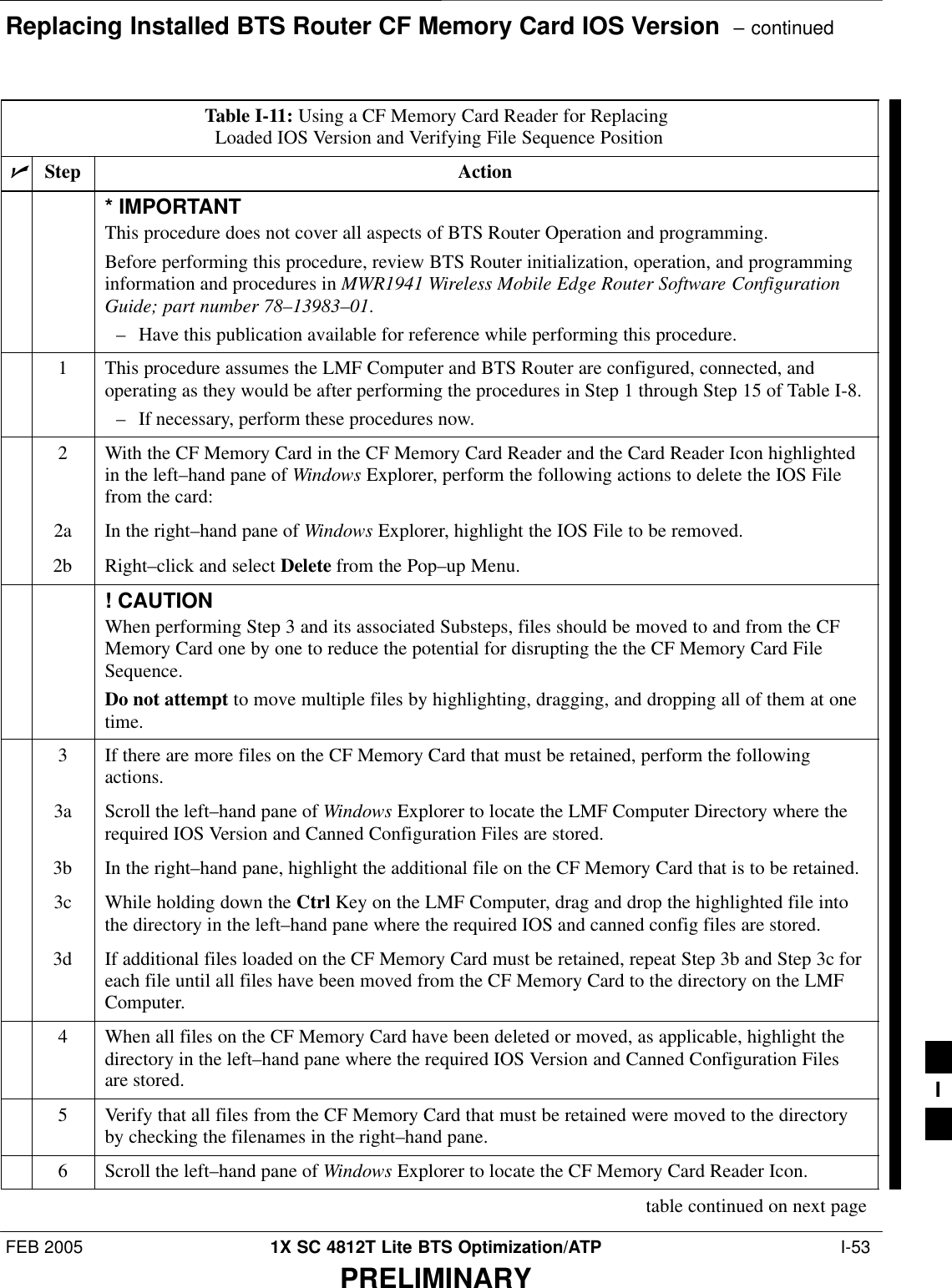
![Replacing Installed BTS Router CF Memory Card IOS Version – continuedFEB 2005 1X SC 4812T Lite BTS Optimization/ATP I-55PRELIMINARYTable I-11: Using a CF Memory Card Reader for Replacing Loaded IOS Version and Verifying File Sequence PositionnActionStepNOTEThe current IOS Working Directory defaults to the CF Memory Card (slot0:) Directory unless thepresent Working Directory has been changed by using the cd Command.– Identify the present Working Directory by entering pwd.SIf the present Working Directory has been changed, enter the cd slot0: Command to returnto the default setting.19 Display the Directory Listing of the CF Memory Card by entering the following command.dir– A response similar to the following will be displayed:Router#dir slot0:Directory of slot0:/1 –rw– 7051976 Sep 23 2002 07:24:18 mwr1941–i–mz.122–8.MC2a.bin2 –rw– 2212 Mar 01 1993 00:14:48 canned–config31932416 bytes total (24885606 bytes free)Router#! CAUTIONThe File Sequence on the CF Memory Card can not be verified with Application Programs thatplace the listed file names in alphabetical order (for example, certain UNIX Telnet Applications,UNIX Directory Listing Commands, and Windows File Managers such as Windows Explorer).This portion of the procedure is intended for use only with applications, such as HyperTerminal,that do not list directory contents alphabetically.20 Ensure that the IOS File is the first file listed in the Directory Content Display.SIf it is, proceed to Step 21.SIf it is not,– Perform the procedure in Table I-12.– Then, return to Step 21, below.21 Verify that the BTS Router will boot properly on the IOS and revised Start–up Configuration Filesby entering the following command.reload– A response similar to the following will be displayed:Router#reloadSystem configuration has been modified. Save? [yes/no]: nProceed with reload? [confirm]22 If prompted to save a modified configuration, enter n for “no,” and press the Enter Key.23 When prompted to proceed with reload, press the Enter Key to continue the Reload Operation.table continued on next pageI](https://usermanual.wiki/Nokia-Solutions-and-Networks/T6FE1.User-Manual-3-of-3/User-Guide-520639-Page-273.png)
![Replacing Installed BTS Router CF Memory Card IOS Version – continued I-60 1X SC 4812T Lite BTS Optimization/ATP FEB 2005PRELIMINARYTable I-12: Use CF Memory Card Reader to Place IOS File First in CF Memory Card File SequencenActionStep7Ensure that the required IOS File and Canned Configuration File for the BTS Router are located inthe TFTP Server Root Directory.– Refer to Table I-4, Step 14 or Step 17, as applicable.8Delete files from the CF Memory Card by entering the del filename command.– A response similar to the following will be displayed:–Router#del canned–configDelete filename [canned–config]?9If the Default Filename displayed in the prompt is correct, press the Enter Key to accept it.SIf it is missing or not correct, enter the correct filename.– A response similar to the following will be displayed if the Default Filename is selected:Delete filename [canned–config]? Delete slot0:canned–config? [confirm]10 Press the Enter Key to confirm the deletion.– A response similar to the following will be displayed if the Default Filename is selected:Delete filename [canned–config]? Delete slot0:canned–config? [confirm]Router#11 Confirm the file deletion by entering the dir command.– A response similar to the following will be displayed:Router#dirDirectory of slot0:/ 1 –rw– 7051976 Sep 23 2002 07:24:18 mwr1941–i–mz.122–8.MC2a.bin31932416 bytes total (24887818 bytes free)Router#12 Repeat Step 8 through Step 11 for each file until all files have been deleted from the CF MemoryCard.13 Use the TFTP Server to copy the IOS File from the LMF Computer to the CF Memory Card byentering the following command.copy TFTP:IOS_filename slot0:– Where IOS_filename = required IOS Version filename in the LMF Computer TFTP ServerRoot Directory.– A response similar to the following will be displayed:BTSRTR1#copy TFTP:mwr1941–i–mz.122–8.MC2a.bin slot0:Address or name of remote host []?table continued on next pageI](https://usermanual.wiki/Nokia-Solutions-and-Networks/T6FE1.User-Manual-3-of-3/User-Guide-520639-Page-278.png)
![Replacing Installed BTS Router CF Memory Card IOS Version – continuedFEB 2005 1X SC 4812T Lite BTS Optimization/ATP I-61PRELIMINARYTable I-12: Use CF Memory Card Reader to Place IOS File First in CF Memory Card File SequencenActionStep14 At the prompt for the Remote Host Address or Name, enter the IP Address of the LMF ComputerNIC:100.100.100.1– A response similar to the following will be displayed:BTSRTR1#copy TFTP:mwr1941–i–mz.122–8.MC2a.bin slot0:Address or name of remote host []? 100.100.100.1Destination filename [mwr1941–i–mz.122–8.MC2a.bin]?15 At the prompt for the Destination Filename, press the Enter Key.– A response similar to the following will be displayed:BTSRTR1#copy TFTP:mwr1941–i–mz.122–8.MC2a.bin slot0:Address or name of remote host []? 100.100.100.1Destination filename [mwr1941–i–mz.122–8.MC2a.bin]?Accessing TFTP://100.100.100.1/mwr1941–i–mz.122–8.MC2a.bin...Loading mwr1941–i–mz.122–8.MC2a.bin from 100.100.100.1 (via FastEthernet0/0): !!!!Loading mwr1941–i–mz.122–8.MC2a.bin from 100.100.100.1 (via FastEthernet0/0):!!!!!!!!!!!!!!!!!!!!!!!!!!!!!!!!!!!!!!!!!!!!!!!!!!!!!!!!!!!!!!!!!!!!!!!!!!!!!!!!!!!!!!!!!!!!!!!!!!!!!!!!!!!!!!!!!!!!!!!!!!!!!!!!!!!!!!!!!!!!!!!!!!!!!!!!!!!!!!!!!!!!!!!!!!!!!!!!!!!!!!!!!!!!!!!!!!!!!!!!!!!!!!!!!!!!!!!!!!!!!!!!!!!!!!!!!!!!!!!!!!!!!!!!!!!!!!!!!!!!!!!!!!!!!!!!!!!!!!!!!!!!!!!!!!!!!!!!!!!!!!!!!!!!!!!!!!!!!!!!!!!!!!!!!!!!!!!!!!!!!!!!!!!!!!!!!!!!!!!!!!!!!!!!!!!!!!!!!!!!!!!!!!!!!!!!!!!!!!!!!!!!!!!!!!!!!!!!!!!!!!!!!!!!!!!!!!!!!!!!!!!!!!!!!!!!!!!!!!!!!!!!!!!!!!!!!!!!!!!!!!!!!!!!!!!!!!!!!!!!!!!!!!!!!!!!!!!!!!!!!!!!!!!!!!!!!!!!!!!!!!!!!!!!!!!!!!!!!!!!!!!!!!!!!!!!!!!!!!!!!!!!!!!!!!!!!!!!!!!!!!!!!!!!!!!!!!!!!!!!!!!!!!!!!!!!!!!!!!!!!!!!!!!!!!!!!!!!!!!!!!!!!!!!!!!!!!!!!!!!!!!!!!!!!!!!!!!!!!!!!!!!!!!!!!!!!!!!!!!!!!!!!!!!!!!!!!!!!!!!!!!!!!!!!!!!!!!!!!!!!!!!!!!!!!!!!!!!!!!!!!!!!!!!!!!!!!!!!!!!!!!!!!!!!!!!!!!!!!!!!!!!!!!!!!!!!!!!!!!!!!!!!!!!!!!!!!!!!!!!!!!!!!!!!!!!!!!!!!!!!!!!!!!!!!!!!!!!!!!!!!!!!!!!!!!!!!!!!!!!!!!!!!!!!!!!!!!!!!!!!!!!!!!!!!!!!!!!!!!!!!!!!!!!!!!!!!!!!!!!!!!!!!!!!!!!!!!!!!!!!!!!!!!!!!!!!!!!!!!!!!!!!!!!!!!!!!!!!!!!!!!!!!!!!!!!!!!!!!!!!!!!!!!!!!!!!!!!!!!!!!!!!!!!!!!!!!!!!!!!!!!!!!!!!!!!!!!!!!!!!!!!!!!!!!!!!!!!!!!!!!!!!!!!!!!!!!!!!!!!!!!!!!!!!!!!!!!!!!!!!!!!!!!!!!!!!!!!!!!!!!!!!!!!!!!!!!!!!!!!!!!!!!!!!!!!!!!!!!!!!!!!!!!!!!!!!!!!!!!!!!!!!!!!!!!!!!!!!!!!!!!!!!!!!!!!!!!!!!!!!!!!!!!!!!!!!!!!!!!!!!!!!!!!!!!!!!!!!!!!!!!!!!!!!!!!!!!!!!!!!!!!!!!!!!!!!!!!!![OK – 7051976/14103552 bytes]7051976 bytes copied in 145.108 secs (48634 bytes/sec)16 Display the directory of the CF Memory Card to confirm the IOS File Transfer by entering the dirCommand.– A response similar to the following will be displayed:Router#dirDirectory of slot0:/ 1 –rw– 7051976 Sep 23 2002 07:24:18 mwr1941–i–mz.122–8.MC2a.bin31932416 bytes total (248880440 bytes free)Router#table continued on next pageI](https://usermanual.wiki/Nokia-Solutions-and-Networks/T6FE1.User-Manual-3-of-3/User-Guide-520639-Page-279.png)
![Replacing Installed BTS Router CF Memory Card IOS Version – continued I-62 1X SC 4812T Lite BTS Optimization/ATP FEB 2005PRELIMINARYTable I-12: Use CF Memory Card Reader to Place IOS File First in CF Memory Card File SequencenActionStep17 Copy the Canned Configuration File to the CF Memory Card by entering the following command.copy TFTP:btsrtr_canned.color slot0:canned–config– Where color = blue or red, as applicable.– A response similar to the following will be displayed:BTSRTR1#copy TFTP:btsrtr_canned.blue slot0:canned–configAddress or name of remote host [100.100.100.1]?18 If the Default IP Address for the LMF Computer displayed in the prompt is correct, press theEnter Key to accept it.SIf it is missing or not correct, enter the correct IP Address.– A response similar to the following will be displayed if the Default Filename is accepted:Destination filename [canned–config]? 2212 bytes copied in 0.208 secsRouter#19 At the prompt for the Destination Filename, press the Enter Key.– A response similar to the following will be displayed:BTSRTR1#copy TFTP:btsrtr_canned.blue slot0:canned–configAddress or name of remote host []? 100.100.100.1Destination filename [canned–config]?Loading btsrtr_canned.blue from 100.100.100.1 (via Ethernet0/0): ![OK – 2457/4096 bytes]2457 bytes copied in 84.724 secs (29 bytes/sec)BTSRTR1#20 Determine if the IOS File is now the first file displayed in the Directory Listing by entering thedir Command.– A response similar to the following will be displayed:Router#dirDirectory of slot0:/ 1 –rw– 7051976 Mar 01 1993 00:14:48 mwr1941–i–mz.122–8.MC2a.bin 2 –rw– 2212 Sep 23 2002 07:24:18 canned–config31932416 bytes total (24878228 bytes free)Router#21 Identify if the IOS File is the first file displayed, as shown in Step 20, above.SIf it is the the first file displayed, proceed to Step 29.SIf it is not the the first file displayed, proceed to Step 22.table continued on next pageI](https://usermanual.wiki/Nokia-Solutions-and-Networks/T6FE1.User-Manual-3-of-3/User-Guide-520639-Page-280.png)
![Replacing Installed BTS Router CF Memory Card IOS Version – continuedFEB 2005 1X SC 4812T Lite BTS Optimization/ATP I-63PRELIMINARYTable I-12: Use CF Memory Card Reader to Place IOS File First in CF Memory Card File SequencenActionStep22 Format the CF Memory Card by entering the following command.format slot0:– A response similar to the following will be displayed:BTSRTR1#format slot0:Format operation may take a while. Continue? [confirm]23 Press the Enter Key to continue the Format Operation.– A response similar to the following will be displayed:Format operation may take a while. Continue? [confirm]Format operation will destroy all data in ”slot0:”. Continue? [confirm]24 Press the Enter Key to continue the Format Operation.– A response similar to the following will be displayed:Format operation will destroy all data in ”slot0:”. Continue? [confirm]Format: Drive communication & 1st Sector Write OK...Writing Monlibsectors....................................................................................Monlib write complete.Format: All system sectors written. OK...Format: Total sectors in formatted partition: 62560Format: Total bytes in formatted partition: 32030720Format: Operation completed successfully.Format of slot0 completeBTSRTR1#25 If a TFTP Server is available on the LMF Computer, repeat Steps 13 through 21 to transfer theIOS and Canned Configuration Files to the CF Memory Card.26 Once the Format Operation is completed, perform the following actions.26a Remove the CF Memory Card from the BTS Router by performing the procedure in the 1XSC4812T Lite BTS FRU manual (68P09262A60).26b Insert the CF Memory Card in the Card Reader connected to the LMF Computer.26c Copy the IOS File to the card by performing Step 4, and Step 6 through Step 11 of Table I-11, asrequired.27 Remove the CF Memory Card from the Card Reader and install it in the BTS Router byperforming the procedure in the 1X SC4812T Lite BTS FRU manual (68P09262A60).table continued on next page I](https://usermanual.wiki/Nokia-Solutions-and-Networks/T6FE1.User-Manual-3-of-3/User-Guide-520639-Page-281.png)
![Verify and Upgrade ROMMON Version – continuedFEB 2005 1X SC 4812T Lite BTS Optimization/ATP I-67PRELIMINARYTable I-13: Verify and Replace the Installed ROMMON Version using a TFTP ServernStep Action* IMPORTANTThis procedure does not cover all aspects of BTS Router Operation and programming.Before performing this procedure, review BTS Router initialization, operation, and programminginformation and procedures in MWR1941 Wireless Mobile Edge Router Software ConfigurationGuide; part number 78–13983–01.– Have this publication available for reference while performing this procedure.1This procedure assumes the LMF Computer and BTS Router are configured, connected, andoperating as they would be after performing the procedures in Table I-4, Table I-5, Table I-6, andSteps 1 through 4 of Table I-7.– If necessary, perform these procedures now.2Identify the installed ROMMON Version from the BTS Router Privileged EXEC Mode Prompt:show version– A response similar to the following will be displayed:BTSRTR1#sh verCisco Internetwork Operating System Software IOS (tm) 1941 Software (MWR1941–I–M), Version 12.2(8)MC2b, EARLY DEPLOYMENT RE-LEASE SOFTWARE (fc3)TAC Support: http://www.cisco.com/tacCopyright (c) 1986–2002 by cisco Systems, Inc.Compiled Mon 05–Aug–02 11:07 by nmasaImage text–base: 0x60008940, data–base: 0x60B54000ROM: System Bootstrap, Version 12.2(20020113:235343) [sbose–wilma 109], DEVELOP-MENT SOFTWAREROM: 1941 Software (MWR1941–I–M), Version 12.2(8)MC2b, EARLY DEPLOYMENT RELEASESOFTWARE (fc3)Router uptime is 1 minuteSystem returned to ROM by power–onSystem image file is ”slot0:mwr1941–i–mz.122–8.MC2b.bin”cisco mwr1941 (R7000) processor (revision 0.1) with 121856K/18432K bytes ofmemory.Processor board ID JMX0611K5TSR7000 CPU at 240Mhz, Implementation 39, Rev 3.3, 256KB L2 CacheBridging software.X.25 software, Version 3.0.0.Primary Rate ISDN software, Version 1.1.Toaster processor tmc is running.2 FastEthernet/IEEE 802.3 interface(s)2 Serial network interface(s)2 Channelized T1/PRI port(s)DRAM configuration is 64 bits wide with parity disabled.55K bytes of non–volatile configuration memory.31360K bytes of ATA Slot0 CompactFlash (Read/Write)Configuration register is 0x101BTSRTR1#table continued on next pageI](https://usermanual.wiki/Nokia-Solutions-and-Networks/T6FE1.User-Manual-3-of-3/User-Guide-520639-Page-285.png)
![Verify and Upgrade ROMMON Version – continued I-68 1X SC 4812T Lite BTS Optimization/ATP FEB 2005PRELIMINARYTable I-13: Verify and Replace the Installed ROMMON Version using a TFTP ServernActionStep3To identify the currently installed ROMMON Version, examine the ROM: system bootstrapLine in the response.4Compare the installed ROMMON Version information with the Filename of the ROMMONVersion required for the network.NOTE1. The ROMMON Filename Format is similar to the following:MWR1941_RM2.srec.122–8r.MC3.bin2. The ROMMON Filename reflects the Version Number of the software (122–8r.MC3).5If the installed version is the one required for the network, skip to Step 26.6If the installed ROMMON Version is not the one required for the network, back–up the currentBTS Router Configuration to the LMF Computer by entering the following command.copy nvram:startup–config TFTP– A response similar to the following will be displayed:BTSRTR1#copy nvram:start TFTPAddress or name of remote host []?NOTEEnsure to include the colon (:) after nvram when typing the command.7At the prompt for the Remote Host Address or Name, enter the IP Address of the LMF ComputerNIC:100.100.100.1– A response similar to the following will be displayed:BTSRTR1#copy copy nvram:start TFTPAddress or name of remote host []? 100.100.100.1Source filename [startup–config]?8If the Default Filename displayed in the prompt is correct, press the Enter Key to accept it.SIf it is missing or not correct, enter the correct filename.– A response similar to the following will be displayed if the Default Filename is selected:Source filename [startup–config]? Destination filename [startup–config]?table continued on next pageI](https://usermanual.wiki/Nokia-Solutions-and-Networks/T6FE1.User-Manual-3-of-3/User-Guide-520639-Page-286.png)
![Verify and Upgrade ROMMON Version – continuedFEB 2005 1X SC 4812T Lite BTS Optimization/ATP I-69PRELIMINARYTable I-13: Verify and Replace the Installed ROMMON Version using a TFTP ServernActionStep9If the Default Filename displayed in the prompt is correct, press the Enter Key to accept it.SIf it is missing or not correct, enter the correct filename.– A response similar to the following will be displayed:Destination filename [startup–config]?![OK – 2212/4096 bytes]2212 bytes copied in 0.152 secsBTSRTR1#NOTEThe IOS defaults to the CF Memory Card (slot0:) Directory unless the present Working Directoryhas been changed by using the cd Command.– Identify the present Working Directory by entering pwd.– If the present Working Directory has been changed, enter the command cd slot0: to returnto the default setting.10 Determine the amount of memory available (bytes free) on the CF Memory Card by entering thedir command.– A response similar to the following will be displayed:BTSRTR1#dirDirectory of slot0:/1 –rw– 7051976 Sep 23 2002 07:24:18 mwr1941–i–mz.122–8.MC2b.bin2 –rw– 2212 Mar 01 1993 00:14:48 canned–config31932416 bytes total (24885606 bytes free)Router#11 Verify that there is at least 1 MB (1048580) of free memory.NOTEA ROMMON Version File requires approximately 0.7 MB.12 Begin to copy the required version of the ROMMON File from the LMF Computer to the BTSRouter by entering the following command.copy TFTP:new_rommon_filename slot0:– Where new_rommon_filename = the filename of the required ROMMON Version for theBTS Router.– A response similar to the following will be displayed:BTSRTR1#copy TFTP:MWR1941_RM2.srec.122–8r.MC3.bin slot0:Address or name of remote host [100.100.100.1]?table continued on next pageI](https://usermanual.wiki/Nokia-Solutions-and-Networks/T6FE1.User-Manual-3-of-3/User-Guide-520639-Page-287.png)
![Verify and Upgrade ROMMON Version – continued I-70 1X SC 4812T Lite BTS Optimization/ATP FEB 2005PRELIMINARYTable I-13: Verify and Replace the Installed ROMMON Version using a TFTP ServernActionStep13 If the Default IP Address displayed in the prompt is correct, press the Enter Key to accept it.SIf it is missing or not correct, enter the correct IP Address for the LMF Computer.– A response similar to the following will be displayed if the Default Filename is selected:Address or name of remote host [100.100.100.1]? Source filename [MWR1941_RM2.srec.122–8r.MC3.bin]?14 If the Default Filename displayed in the prompt is correct, press the Enter Key to accept it.SIf it is missing or not correct, enter the correct filename.– A response similar to the following will be displayed if the Default Filename is selected:Source filename [MWR1941_RM2.srec.122–8r.MC3.bin]? Destination filename [MWR1941_RM2.srec.122–8r.MC3.bin]?15 If the Default Filename displayed in the prompt is correct, press the Enter Key to accept it.SIf it is not correct, enter the correct filename.– A response similar to the following will be displayed if the Default Filename is selected:Destination filename [MWR1941_RM2.srec.122–8r.MC3.bin]? Accessing TFTP://100.100.100.1/MWR1941_RM2.srec.122–8r.MC3.bin...Loading MWR1941_RM2.srec.122–8r.MC3.bin from 100.100.100.1 (via FastEthernet0/0):!!!!Loading MWR1941_RM2.srec.122–8r.MC3.bin from 100.100.100.1 (via FastEthernet0/0):!!!!!!!!!!!!!!!!!!!!!!!!!!!!!!!!!!!!!!!!!!!!!!!!!!!!!!!!!!!!!!!!!!!!!!!!!!!!!!!!!!!!!!!!!!!!!!!!!!!!!!!!!!!!!!!!!!!!!!!!!![OK – 614306/14103552 bytes]614306 bytes copied in 13.059 secs (48634 bytes/sec)BTSRTR1#16 Display the CF Memory Card Directory to verify that the new ROMMON Version File is there byentering the dir Command.– A response similar to the following will be displayed:BTSRTR1#dirDirectory of slot0:/ 1 –rw– 7051976 Sep 23 2002 07:25:36 mwr1941–i–mz.122–8.MC2b.bin 2 –rw– 2212 Mar 01 1993 00:09:06 canned–config 3 –rw– 614306 Dec 13 2002 14:59:36 MWR1941_RM2.srec.122–8r.MC3.bin31932416 bytes total (24263922 bytes free)BTSRTR1#17 Replace the existing ROMMON Version with the new one copied to the CF Memory Card byentering the following command.upgrade rom–monitor file slot0:MWR1941_RM2.srec.122–8r.MC3– A response similar to the following will be displayed:BTSRTR1#This command will reload the BTS Router. Continue?[yes/no]table continued on next pageI](https://usermanual.wiki/Nokia-Solutions-and-Networks/T6FE1.User-Manual-3-of-3/User-Guide-520639-Page-288.png)
![Verify and Upgrade ROMMON Version – continuedFEB 2005 1X SC 4812T Lite BTS Optimization/ATP I-71PRELIMINARYTable I-13: Verify and Replace the Installed ROMMON Version using a TFTP ServernActionStep18 When prompted to continue, enter yes and press the Enter Key.– A response similar to the following will be displayed:BTSRTR1#This command will reload the BTS Router. Continue?[yes/no] yesROMMON image upgrade in progressErasing boot flasheeeeeeeeeeeeeeeeeeeeeeeeeeeeeeeeeeeeeeeeeeeeeeeeeeeeeeeeeeeeeeeeeeProgramming boot flash ppppNow reloading19 When the BTS Router has completed Initialization, change to the BTS Router Privileged EXECMode by entering the following command.enable– A response similar to the following will be displayed:BTSRTR1>enableBTSRTR1#20 Verify that the BTS Router has initialized with the new ROMMON Version by entering thefollowing command.show version– A response similar to the following partial response will be displayed:BTSRTR1#sh verCisco Internetwork Operating System Software IOS (tm) 1941 Software (MWR1941–I–M), Version 12.2(8)MC2b, EARLY DEPLOYMENT RE-LEASE SOFTWARE (fc3)TAC Support: http://www.cisco.com/tacCopyright (c) 1986–2002 by cisco Systems, Inc.Compiled Mon 05–Aug–02 11:07 by nmasaImage text–base: 0x60008940, data–base: 0x60B54000ROM: System Bootstrap, Version 12.2(8r)MC3 RELEASE SOFTWARE (fc1)21 Compare the version displayed in the response ROM: System Bootstrap Line to the filename ofthe new ROMMON Version File copied to the CF Memory Card.22 If the BTS Router successfully rebooted with the new ROMMON Version, the ROMMON Filecan be deleted from the CF Memory Card by entering the following command.delete slot0:new_rommon_filename– Where new_rommon_filename = the filename of the required ROMMON Version copied tothe CF Memory Card in Steps 12 through 15, above.– A response similar to the following will be displayed:BTSRTR1#del slot0:MWR1941_RM2.srec.122–8r.MC3.binDelete filename [MWR1941_RM2.srec.122–8r.MC3.bin]?table continued on next pageI](https://usermanual.wiki/Nokia-Solutions-and-Networks/T6FE1.User-Manual-3-of-3/User-Guide-520639-Page-289.png)
![Verify and Upgrade ROMMON Version – continued I-72 1X SC 4812T Lite BTS Optimization/ATP FEB 2005PRELIMINARYTable I-13: Verify and Replace the Installed ROMMON Version using a TFTP ServernActionStep23 If the Default Filename displayed in the prompt is correct, press the Enter Key to accept it.SIf it is missing or not correct, enter the correct filename.– A response similar to the following will be displayed if the Default Filename is selected:Delete filename [MWR1941_RM2.srec.122–8r.MC3.bin]? Delete slot0:MWR1941_RM2.srec.122–8r.MC3.bin? [confirm]24 Press the Enter Key to confirm the deletion.– A response similar to the following will be displayed if the Default Filename is selected:Delete filename [MWR1941_RM2.srec.122–8r.MC3.bin]? Delete slot0:MWR1941_RM2.srec.122–8r.MC3.bin? [confirm]BTSRTR1#! CAUTIONIn Step 25, do not delete the IOS and canned–config files from the CF Memory Card.– The BTS Router must have these files on the card to properly boot or switch between Packetand Circuit Mode.25 If additional unnecessary files, such as a back–up of the startup–config File, are also on theCF Memory Card, delete them by repeating Step 22 through Step 24 for each file.26 If no other BTS Router File Operations or Configuration Actions are required, perform thefollowing actions.26a Remove power from the BTS Router and disconnect it from the Power Supply Module.26b Disconnect all cabling from the BTS Router.26c On the LMF Computer, exit the HyperTerminal Communications Session.27 If no additional TFTP Transfer activities will be performed, change the NIC IP Address andSubnet Mask back to those for LMF–BTS Communication recorded in Table I-4, Step 9b.! CAUTIONIf the BTS 10base–2 LAN IP Address and Subnet Mask for the LMF Computer’s NIC are notrestored, the LMF can not log into a BTS when attempting to perform a BTS Optimization orATP. Method 2: Verification andReplacement of InstalledROMMON Version Using a CFMemory Card ReaderDescriptionThis procedure covers using an LMF Computer equipped with a CFMemory Card Reader to perform the following activities.:1. Verify the ROMMON Version loaded and running on a BTS Router.2. Replace the ROMMON Version installed in a BTS Router.I](https://usermanual.wiki/Nokia-Solutions-and-Networks/T6FE1.User-Manual-3-of-3/User-Guide-520639-Page-290.png)
![Verify and Upgrade ROMMON Version – continued I-74 1X SC 4812T Lite BTS Optimization/ATP FEB 2005PRELIMINARYTable I-14: Verify and Replace the Installed ROMMON Version using a CF Memory Card ReadernStep Action* IMPORTANTThis procedure does not cover all aspects of BTS Router Operation and programming.Before performing this procedure, review BTS Router initialization, operation, and programminginformation and procedures in MWR1941 Wireless Mobile Edge Router Software ConfigurationGuide; part number 78–13983–01.– Have this publication available for reference while performing this procedure.1This procedure assumes the LMF Computer and BTS Router are configured, connected, andoperating as they would be after performing the procedures in Step 1 through Step 10 of Table I-8.– If necessary, perform these procedures now.2Determine the currently installed ROMMON Version by entering the following at the BTS RouterPrivileged EXEC Mode Prompt:show version– A response similar to the following will be displayed:BTSRTR1#sh verCisco Internetwork Operating System Software IOS (tm) 1941 Software (MWR1941–I–M), Version 12.2(8)MC2b, EARLY DEPLOYMENT RE-LEASE SOFTWARE (fc3)TAC Support: http://www.cisco.com/tacCopyright (c) 1986–2002 by cisco Systems, Inc.Compiled Mon 05–Aug–02 11:07 by nmasaImage text–base: 0x60008940, data–base: 0x60B54000ROM: System Bootstrap, Version 12.2(20020113:235343) [sbose–wilma 109], DEVELOP-MENT SOFTWAREROM: 1941 Software (MWR1941–I–M), Version 12.2(8)MC2b, EARLY DEPLOYMENT RELEASESOFTWARE (fc3)Router uptime is 1 minuteSystem returned to ROM by power–onSystem image file is ”slot0:mwr1941–i–mz.122–8.MC2b.bin”cisco mwr1941 (R7000) processor (revision 0.1) with 121856K/18432K bytes ofmemory.Processor board ID JMX0611K5TSR7000 CPU at 240Mhz, Implementation 39, Rev 3.3, 256KB L2 CacheBridging software.X.25 software, Version 3.0.0.Primary Rate ISDN software, Version 1.1.Toaster processor tmc is running.2 FastEthernet/IEEE 802.3 interface(s)2 Serial network interface(s)2 Channelized T1/PRI port(s)DRAM configuration is 64 bits wide with parity disabled.55K bytes of non–volatile configuration memory.31360K bytes of ATA Slot0 CompactFlash (Read/Write)Configuration register is 0x101BTSRTR1#table continued on next pageI](https://usermanual.wiki/Nokia-Solutions-and-Networks/T6FE1.User-Manual-3-of-3/User-Guide-520639-Page-292.png)
![Verify and Upgrade ROMMON Version – continuedFEB 2005 1X SC 4812T Lite BTS Optimization/ATP I-75PRELIMINARYTable I-14: Verify and Replace the Installed ROMMON Version using a CF Memory Card ReadernActionStep3To determine the currently installed ROMMON Version, examine the ROM: System BootstrapLine in the response.4Compare the installed ROMMON Version Information with the Filename of the ROMMONVersion required for the network.NOTE1. The ROMMON Filename Format is similar to the following:MWR1941_RM2.srec.122–8r.MC3.bin2. The ROMMON Filename reflects the Version Number of the software (122–8r.MC3).5If the installed version is the one required for the network, skip to Step 26.6NOTEThe IOS defaults to the CF Memory Card (slot0:) directory unless the present Working Directoryhas been changed by using the cd Command.– Identify the present Working Directory by entering pwd.SIf the present Working Directory has been changed, enter the command cd slot0: to return tothe default setting.7If the installed ROMMON Version is not the one required for the network, determine the amountof memory available (bytes free) on the CF Memory Card by entering the following command.dir– A response similar to the following will be displayed:BTSRTR1#dirDirectory of slot0:/ 1 –rw– 7051976 Sep 23 2002 07:24:18 mwr1941–i–mz.122–8.MC2b.bin 2 –rw– 2212 Mar 01 1993 00:14:48 canned–config31932416 bytes total (24885606 bytes free)Router#8Ensure that there is at least 1 MB (1048580) of free memory.NOTEA ROMMON Version File requires approximately 0.7 MB, and space must also be available for aback–up of the BTS Router’s startup–config File.9Create a back–up of the current BTS Router Configuration on the CF Memory Card by enteringthe following command.copy nvram:startup–config slot:0– A response similar to the following will be displayed:BTSRTR1#copy nvram:startup–config slot0:Destination filename [startup–config]?table continued on next pageI](https://usermanual.wiki/Nokia-Solutions-and-Networks/T6FE1.User-Manual-3-of-3/User-Guide-520639-Page-293.png)
![Verify and Upgrade ROMMON Version – continued I-76 1X SC 4812T Lite BTS Optimization/ATP FEB 2005PRELIMINARYTable I-14: Verify and Replace the Installed ROMMON Version using a CF Memory Card ReadernActionStep10 If the Default Filename displayed in the prompt is correct, press the Enter Key to accept it.SIf it is missing or not correct, enter the correct filename.– A response similar to the following will be displayed:Destination filename [startup–config]? 2212 bytes copied in 4.96 secs (553 bytes/sec)BTSRTR1#11 Remove the CF Memory Card from the BTS Router by performing the procedure in the 1XSC4812T Lite BTS FRU manual (68P09262A60).12 Insert the CF Memory Card into the Card Reader as specified by the Card Reader manufacturer’sinstructions.13 On the LMF Computer, click Start > Programs > Windows Explorer to open Windows Explorer.NOTEThe CF Memory Card Reader will appear as a Disk Drive in Windows Explorer with a Disk Driveletter and icon.14 Scroll the left–hand pane of Windows Explorer to locate the icon for the CF Memory Card.15 In the left–hand pane of WindowsExplorer, highlight the CF Memory Card Icon.16 In the right–hand pane, verify that the files displayed in Step 6, above, appear.17 Scroll the left–hand pane of Windows Explorer to locate the icon for the directory where therequired ROMMON Version File is stored.18 In the right–hand pane, perform the following actions.18a Highlight the startup–config File on the CF Memory Card.NOTEAfter highlighting the startup–config File in the right–hand pane, it may be necessary to scrollthe left–hand pane to see the Directory Icon where the required ROMMON Version File is storedbefore dragging the file.18b Note its file size.18c Drag it to the icon for the directory where the required ROMMON Version File is stored.19 In the left–hand pane, highlight the directory where the required ROMMON Version File is stored.20 In the right–hand pane, verify that the startup–config File is in the directory, and the file sizeis the same as the original on the CF Memory Card.table continued on next pageI](https://usermanual.wiki/Nokia-Solutions-and-Networks/T6FE1.User-Manual-3-of-3/User-Guide-520639-Page-294.png)
![Recovery from BTS Router Boot to ROMMON – continued I-80 1X SC 4812T Lite BTS Optimization/ATP FEB 2005PRELIMINARYTable I-15: Simple Recovery from BTS Router ROMMON BootnActionStep3Note the IOS Filename, and enter the following command to begin recovery to an IOS Boot:boot slot0:IOS_filename– Where IOS_filename = the filename of the IOS noted in Step 2, above.– A successful IOS re–boot operation will result in display of a response that begins and endssimilar to the following:rommon 2 > boot slot0:mwr1941–i–mz.122–8.MC2a.binprogram load complete, entry point: 0x80008000, size: 0xb2a0program load complete, entry point: 0x80008000, size: 0x6b99acSelf decompressing the image :################################################################### [OK]Smart Init is enabledsmart init is sizing iomem ID MEMORY_REQ TYPE00031A 0X005F3C00 MWR1941 Mainboard 0X000F3BB0 public buffer pools 0X00211000 public particle poolsTOTAL: 0X008F87B0...Press RETURN to get started!SIf the BTS Router successfully reboots with the IOS, proceed to Step 7.SIf the BTS Router does not reboot with the IOS, proceed to Step 44Scroll the HyperTerminal Display down until the Directory Display from Step 2, above, is visible.5Compare the IOS Filename from the Directory Display with the filename entered in performingStep 3, above.SIf the filename was typed incorrectly, repeat Step 3, using care to type the filename correctly.6If the BTS Router does not reboot with the IOS after typing the filename correctly, proceed toTable I-16 and perform the Extended Recovery Procedure.table continued on next pageI](https://usermanual.wiki/Nokia-Solutions-and-Networks/T6FE1.User-Manual-3-of-3/User-Guide-520639-Page-298.png)
![Recovery from BTS Router Boot to ROMMON – continued I-82 1X SC 4812T Lite BTS Optimization/ATP FEB 2005PRELIMINARYTable I-15: Simple Recovery from BTS Router ROMMON BootnActionStep7f Verify that the correct IOS Filename is now included in the listing by entering the followingcommand.show startup–config– A response that begins similar to the following will be displayed:BTSRTR1#sh startUsing 1589 out of 57336 bytes!version 12.2service timestamps debug uptimeservice timestamps log uptimeno service password–encryption!hostname BTSRTR1!boot system slot0:mwr1941–i–mz.122–8.MC2a.binno logging console!username cisco password 0 cisco!Redundancy mode y–cable standalone!7g If the filename is correctly written, enter the following to determine if the BTS Router will rebootto IOS:reload– A response similar to the following will be displayed:BTSRTR1#reloadSystem configuration has been modified. Save? [yes/no]: nProceed with reload? [confirm]8If prompted to save a modified configuration, enter n for “no,” and press the Enter Key.9When prompted to proceed with reload, press the Enter Key to continue the Reload Operation.10 After a successful reboot with IOS, proceed with other BTS Router activities or remove powerfrom the BTS Router and disconnect it.11 If the BTS Router still will not successfully boot with IOS, proceed to Table I-16 and perform theExtended Recovery Procedure. I](https://usermanual.wiki/Nokia-Solutions-and-Networks/T6FE1.User-Manual-3-of-3/User-Guide-520639-Page-300.png)
![Recovery from BTS Router Boot to ROMMON – continuedFEB 2005 1X SC 4812T Lite BTS Optimization/ATP I-85PRELIMINARYTable I-16: Extended Recovery from BTS Router ROMMON BootnActionStep6Enter the following command to initialize the BTS Router with the IOS on the additional CFMemory Card.boot slot0:IOS_filename– Where IOS_filename = the filename of the IOS noted in Step 5, above.– A successful IOS re–boot operation will result in display of a response that begins and endssimilar to the following:rommon 2 > boot slot0:mwr1941–i–mz.122–8.MC2a.binprogram load complete, entry point: 0x80008000, size: 0xb2a0program load complete, entry point: 0x80008000, size: 0x6b99acSelf decompressing the image :################################################################### [OK]Smart Init is enabledsmart init is sizing iomem ID MEMORY_REQ TYPE00031A 0X005F3C00 MWR1941 Mainboard 0X000F3BB0 public buffer pools 0X00211000 public particle poolsTOTAL: 0X008F87B0... ––– System Configuration Dialog –––Would you like to enter the Initial Configuration dialog? [yes/no]: nSIf the BTS Router Prompts with a question to enter the initial dialog as shown in Step 6, above,type no and press the Enter Key to obtain the User EXEC Mode Prompt.SIf the BTS Router Prompts with Press RETURN to get started!, press the Enter Key toobtain the User EXEC Mode Prompt.7At the User EXEC Mode Prompt, enter the following to access the Privileged EXEC Mode:enableA response similar to the following will be displayed:Router> enableRouter#table continued on next pageI](https://usermanual.wiki/Nokia-Solutions-and-Networks/T6FE1.User-Manual-3-of-3/User-Guide-520639-Page-303.png)
![Recovery from BTS Router Boot to ROMMON – continued I-86 1X SC 4812T Lite BTS Optimization/ATP FEB 2005PRELIMINARYTable I-16: Extended Recovery from BTS Router ROMMON BootnActionStep8Remove the additional CF Memory Card from the BTS Router by performing the procedure in the1X SC4812T Lite BTS FRU manual (68P09262A60).9Install the original CF Memory Card in the BTS Router by performing the procedure in the 1XSC4812T Lite BTS FRU manual (68P09262A60).10 Format the original CF Memory Card by entering the following command.format slot0:A response similar to the following will be displayed:Router#format slot0:Format operation may take a while. Continue? [confirm]11 Press the Enter Key to continue the Format Operation. A response similar to the following willbe displayed:Format operation may take a while. Continue? [confirm]Format operation will destroy all data in ”slot0:”. Continue? [confirm]12 Press the Enter Key to continue the Format Operation. A response similar to the following willbe displayed:Format operation will destroy all data in ”slot0:”. Continue? [confirm]Format: Drive communication & 1st Sector Write OK...Writing Monlibsectors....................................................................................Monlib write complete.Format: All system sectors written. OK...Format: Total sectors in formatted partition: 62560Format: Total bytes in formatted partition: 32030720Format: Operation completed successfully.Format of slot0 completeRouter#13 Copy the required IOS Version to the formatted original CF Memory Card by performing one ofthe following:SUse the LMF Computer and a TFTP Server performing the procedure in Table I-10SUse the LMF Computer and a CF Memory Card Reader performing the procedure in Table I-1114 If applicable, perform IOS initialization troubleshooting as described in Table I-15, Steps 7through 10. I](https://usermanual.wiki/Nokia-Solutions-and-Networks/T6FE1.User-Manual-3-of-3/User-Guide-520639-Page-304.png)
![Entering or Changing Router FE Interface IP Address – continued I-90 1X SC 4812T Lite BTS Optimization/ATP FEB 2005PRELIMINARYTable I-17: Enter/Change BTS Router FE Interface IP Addresses and Operating ParametersnActionStep13 Once the correct parameters have been set for all FE Interfaces, return to the Privileged EXECMode Prompt by holding down the Ctrl Key and pressing z (Ctrl +z).– A response similar to the following will be displayed:BTSRTR–bts#–1–1(config–if)# ^z01:11:27: %SYS–5–CONFIG_I: Configured from console by consoleBTSRTR–bts#–1–1#NOTEEntering exit twice, pressing the Enter Key after each entry, will also complete the InterfaceConfiguration and return the BTS Router to the Privileged EXEC Mode.14 Save the Interface Configuration changes to the Start–up Configuration File on the CF MemoryCard by entering the following command.copy running–config startup–config– A response similar to the following will be displayed:BTSRTR–bts#–1–1# copy run startBTSRTR–bts#–1–1# Destination filename [startup–config]?15 Press Enter.– A response similar to the following will be displayed:BTSRTR–bts#–1–1# copy run startBTSRTR–bts#–1–1# Destination filename [startup–config]?Building configuration...!!!!!!!!!!!!!!!!!!!!!!!!!!!!!!!!!!!!!!!!!!!!!!!!!!!!!!!!!!!!!!!!!!!!!!!!!!!!!!!!!![OK]BTSRTR–bts#–1–1#16 If all FE IP Address Entries/Changes for the BTS Router are complete, enter the following toreturn the BTS Router to user EXEC Mode:disable– A response similar to the following will be displayed:BTSRTR–bts#–1–1# disableBTSRTR–bts#–1–1>17 Determine if any other Router requires the FE Interfaces to be assigned/changed.SIf no other Router requires the FE Interfaces to be assigned/changed, proceed to Step 20.If FE Interfaces on another Router must be assigned/changed, proceed to Step 18.18 Disconnect the 8–contact Modular Plug from the current Router CONSOLE Port and connect it to theCONSOLE Port of the other Router.table continued on next pageI](https://usermanual.wiki/Nokia-Solutions-and-Networks/T6FE1.User-Manual-3-of-3/User-Guide-520639-Page-308.png)