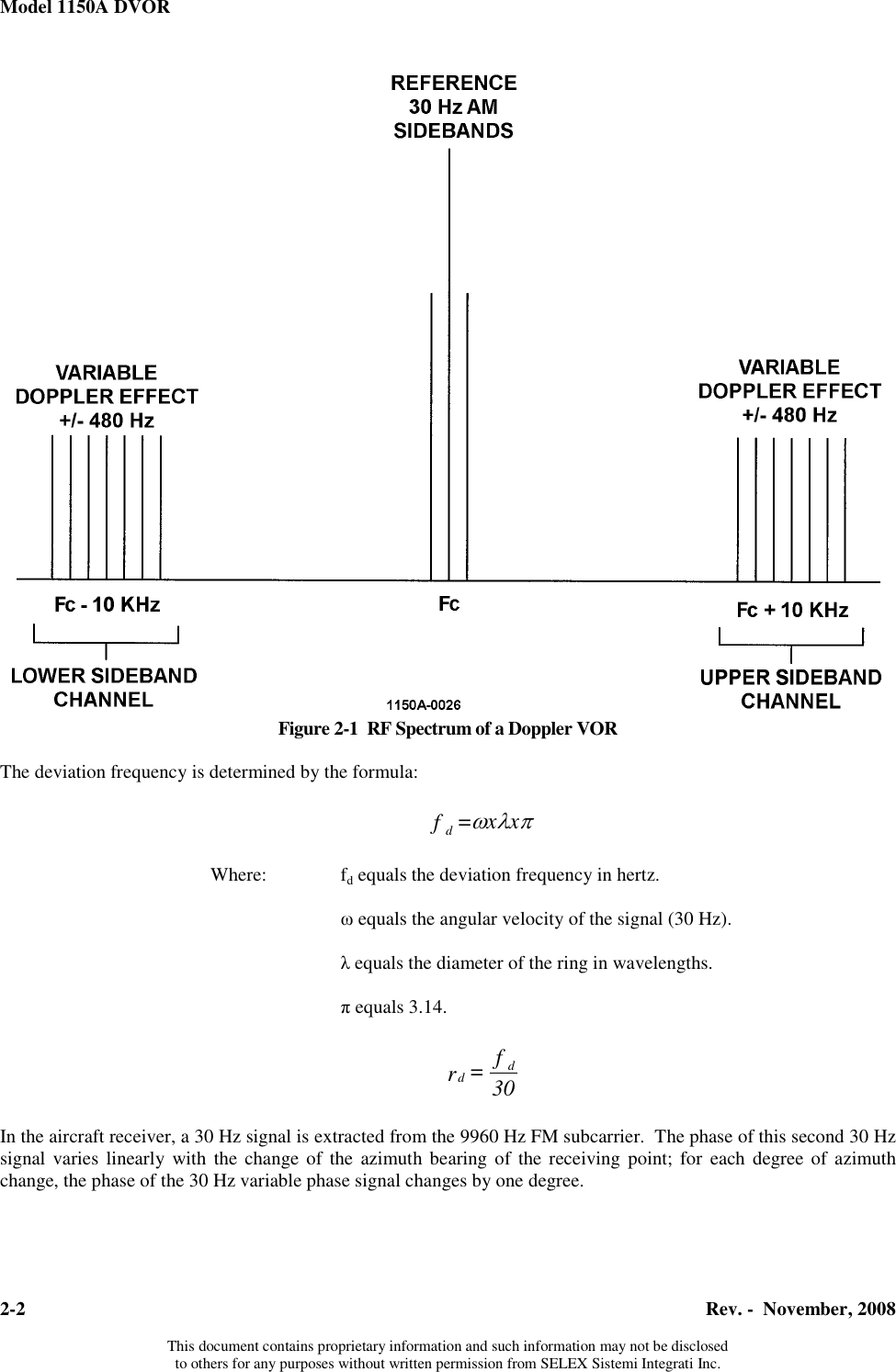
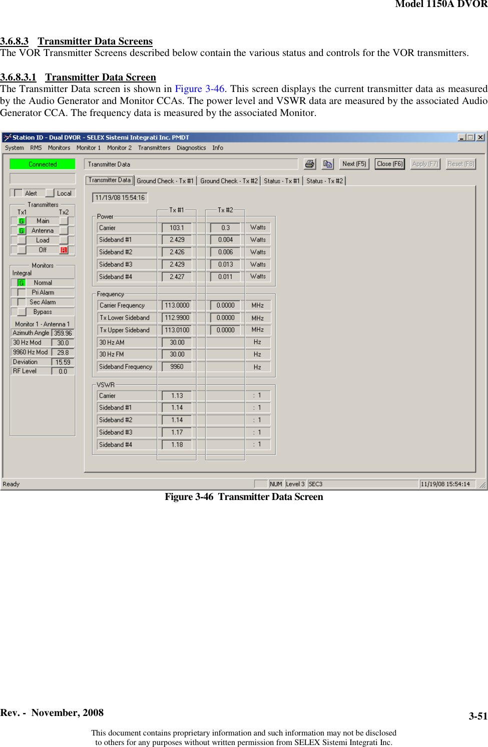
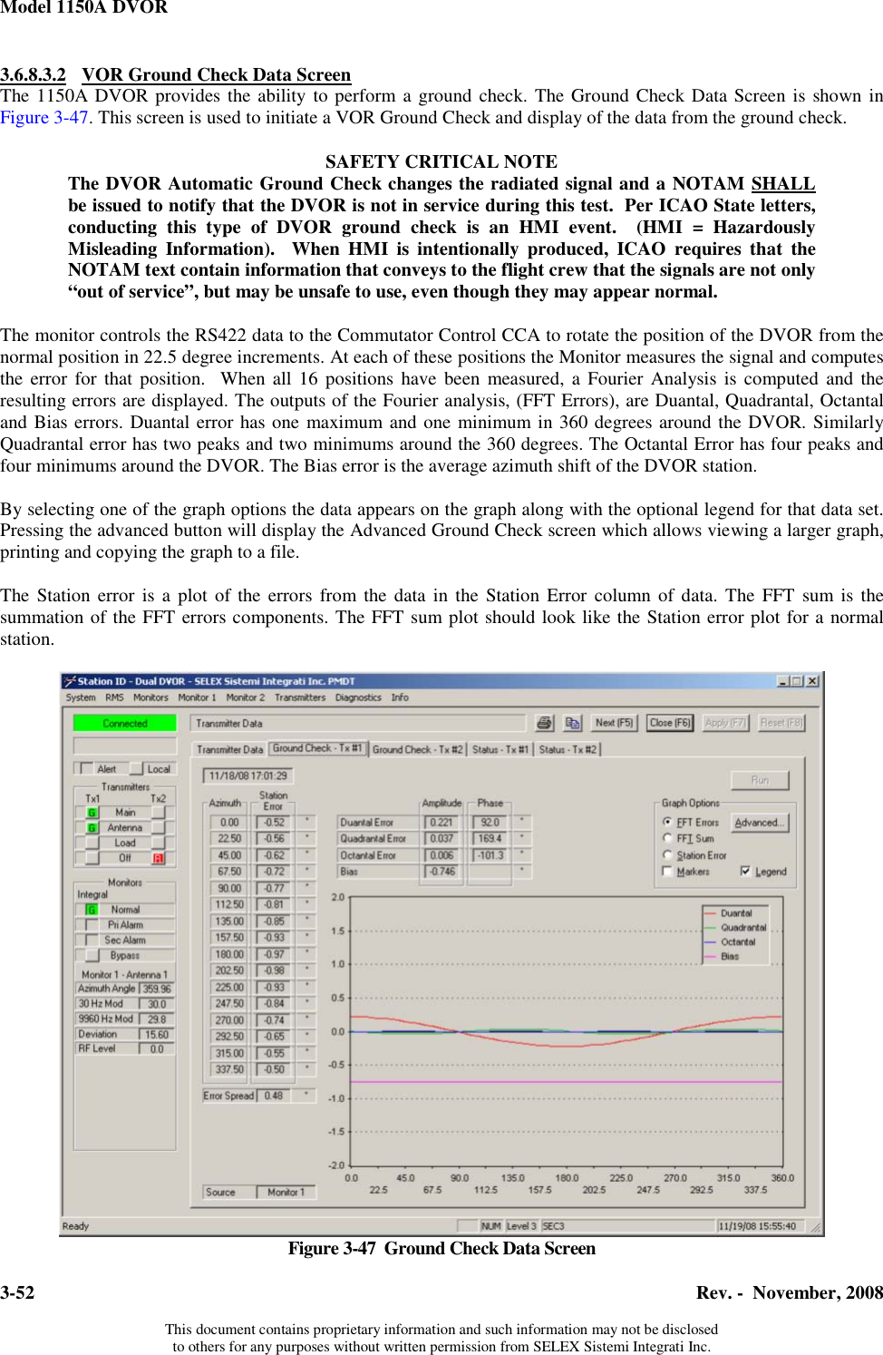
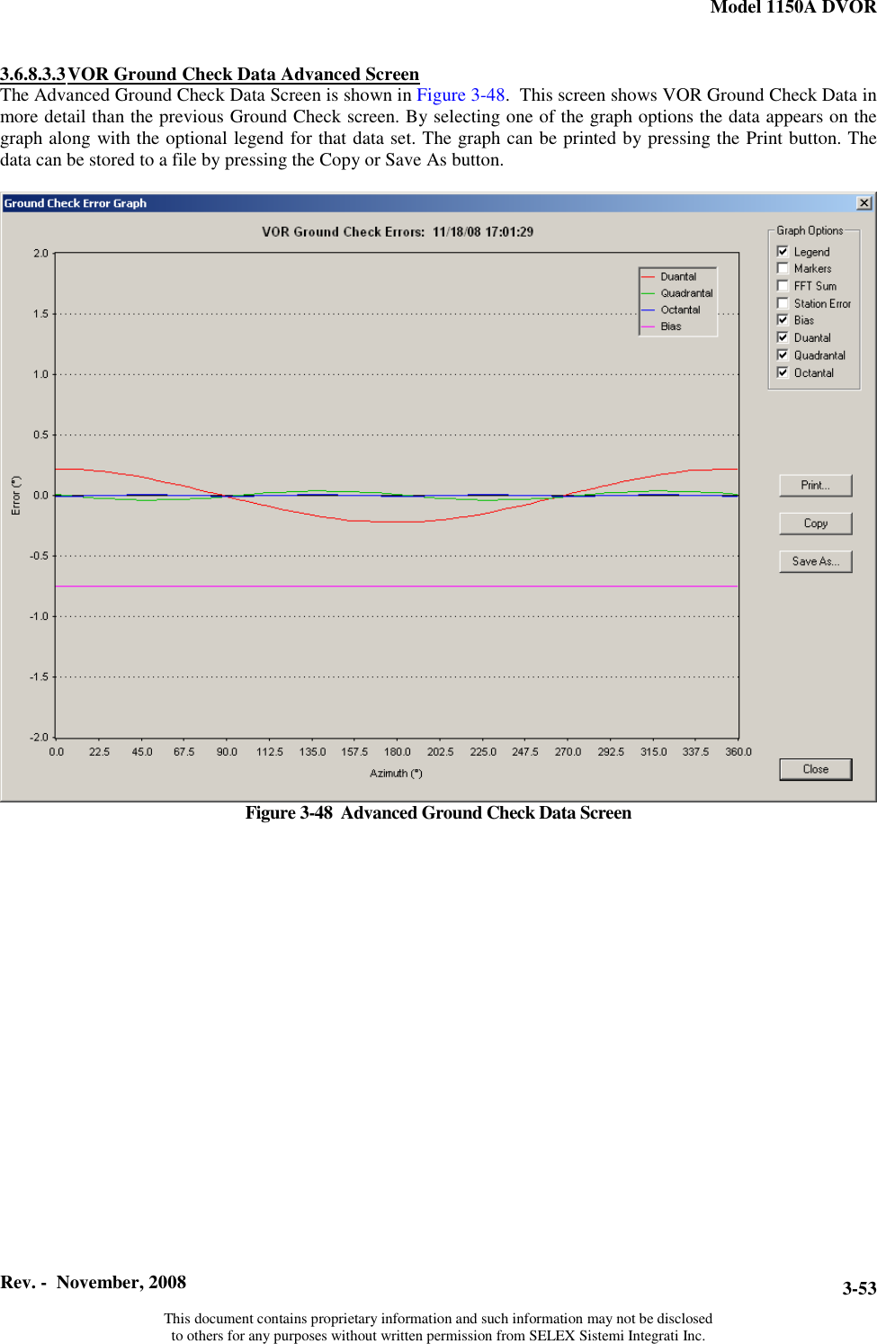
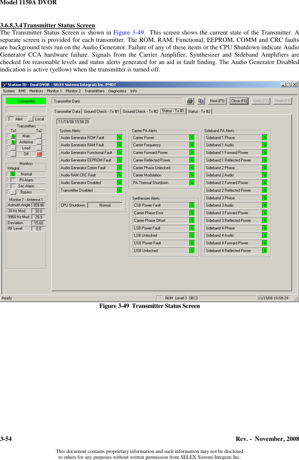
Selex Sistemi Integrati VOR2 VOR Transmitter User Manual 571150A 0002
Selex Sistemi Integrati Inc. VOR Transmitter 571150A 0002
UserManual.wiki
>
Selex Sistemi Integrati
>
VOR2 User Manual
Users Manual
Navigation menu
Upload a User Manual
Namespaces
Wiki Guide
HTML
PDF
Info
Views
User Manual
Discussion / Help
Navigation


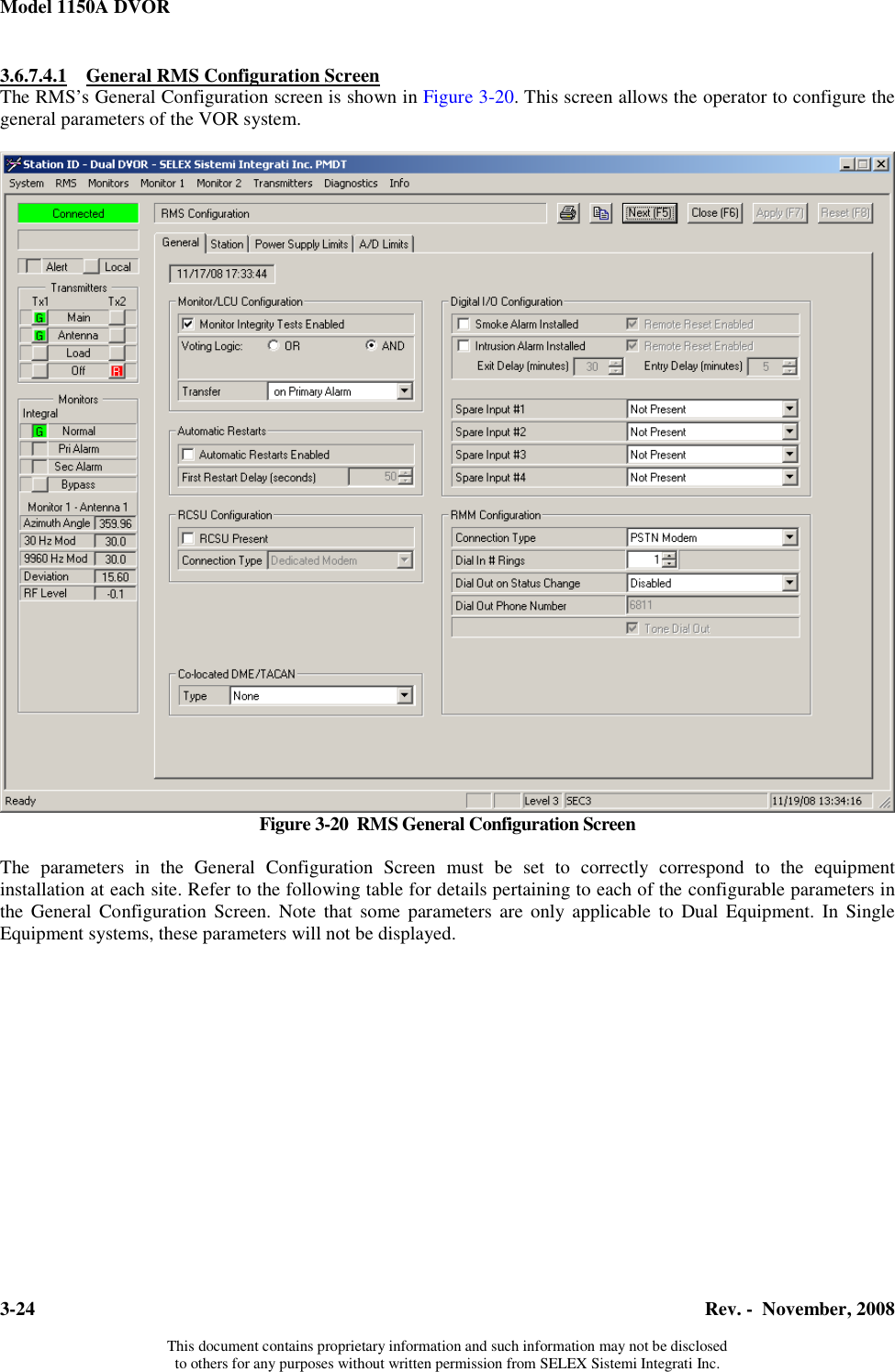
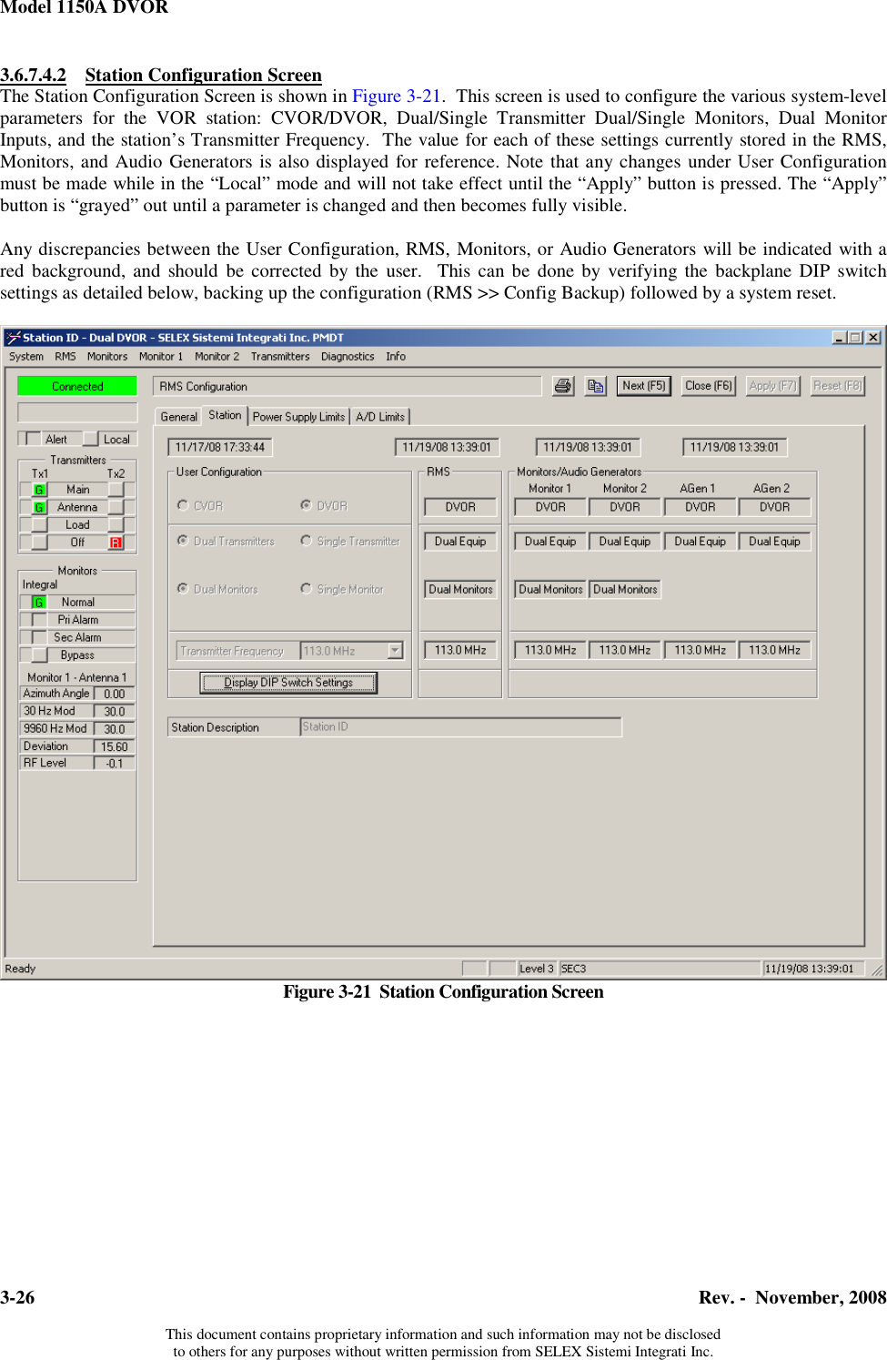
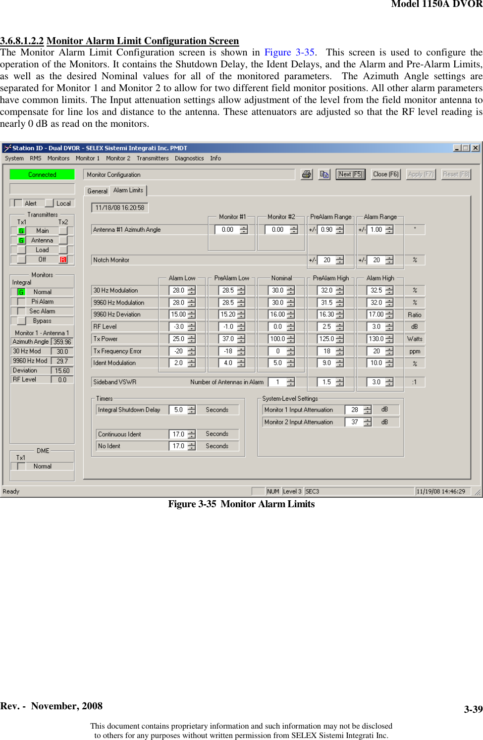
![Model 1150A DVOR Rev. - November, 2008 This document contains proprietary information and such information may not be disclosed to others for any purposes without written permission from SELEX Sistemi Integrati Inc. 3-53.6.4 Screen AreaThe screen area displays selected common parameters and status data. The screen may present tabs and buttons that allow the operator to make further selections. Shortcuts have been implemented in the PMDT allowing keyboard entry of the Next, Close, Apply, and Reset functions. These buttons are enabled as applicable when navigating through the various PMDT screens. When they are enabled, pressing the following function key results in the specified action: F5 Next Move to the next screen in the current group. F6 Close Close the current group of screens. F7 Apply Save the changes made in the current screen. F8 Reset Cancels any changes to the current screen, leaving the data unchanged. The main PMDT screen also contains two buttons that are used as follows: Print Screen - Pressing this button sends a copy of the current PMDT screen, including the Sidebar, to the default printer. This will either be a graphical image or a text-based copy of the screen, depending on how the “Print Screens” option is set in the PMDT Configuration screen shown below. Copy Data to Clipboard - Available only when a block of text is displayed on a screen, such as in the RMS >> Logs screens. Pressing this button copies the text data to the Windows Clipboard, so that the user can paste it into another Windows application such as Notepad. 3.6.5 Configuring the PMDTThe PMDT Configuration screen shown in Figure 3-2 is used to configure the various PMDT options. The direct connection COM port must be configured before any navaid connection can be established. For the VOR navaid, which has a USB-based PMDT connection, this must be set to the associated USB Serial Port. Note that this USB Serial Port is dynamically installed/uninstalled when the USB cable between the PMDT PC and the VOR is connected/disconnected, as well as when the navaid is powered on/off. The Print Screens option allows the user to select either a Graphic Image, or a text-based representation of the screen. The dial-out modem must be selected prior to establishing a modem-based connection to a navaid or RCSU. This should be set to the desired PMDT computer internal modem. Alternatively, a dedicated leased-line modem can be used to establish the RMM link. The desired language for the PMDT GUI may be selected from the available list. Typically, the Local RCSU IP Address and IP Port should be kept at the defaults settings shown below. Refer to the facility’s IT department for the proper settings before making any changes to these settings. The Operational Mode should typically be set to “Normal”. The “Specified Navaid Mode” is used to force the PMDT to connect to a user-specified navaid (eg. Localizer, Glideslope, VOR, etc.) instead of dynamically determining the navaid type during its initial communications with the navaid. Change this setting only if directed by SELEX-SI Customer Service, or the installation instruction in a specialized SELEX-SI RMM equipment kit. When enabled, navaid connection is initiated by selecting the following menu items: System>>Connect>>Specified Navaid>>Serial/USB [or Modem]>>[the desired navaid]](https://usermanual.wiki/Selex-Sistemi-Integrati/VOR2/User-Guide-1103052-Page-125.png)


![Model 1150A DVOR Rev. - November, 2008 This document contains proprietary information and such information may not be disclosed to others for any purposes without written permission from SELEX Sistemi Integrati Inc. 6-11e. Turn on AC/DC power on VOR front panel. f. Place the VOR in LOCAL mode. Select System>> Configuration Load, and select the Filename saved in Step a. g. Select RMS>> Config Backup. h. Set the current date and time by selecting RMS>> Commands>> Set Time and Date, [enter]. 6.4.10 Update of DVOR SoftwareNOTE During the product life cycle software updates may become available for the VOR product in service. The RMS, Monitor and Audio Generator software is updated through the PMDT port using a SELEX-SI software product called “Flash loader” Please refer to the installation instructions accompanying the software update service bulletin for detailed software upgrade procedures. a. On the PMDT Select System>> Configuration Save. Select or create a distinctive filename to save the current system configuration and click save. b. Perform the software update per the instruction provided. c. Place the VOR in LOCAL mode. Select System>> Configuration Load, and select the Filename saved in Step a. d. Select RMS>> Config Backup. e. Set the current date and time by selecting RMS>> Commands>> Set Time and Date, [enter]. 6.4.11 Changing the Station Rotation (Azimuth)This step may be requested during a flight inspection of the VOR station. a. Select Transmitters>> Configuration>> Offsets. Adjust the Azimuth angle offset for Transmitter 1 and/or Transmitter 2. b. Enter a more positive number for clockwise rotation or a more negative number for counterclockwise rotation. The allowable entry is ±180 degrees in 0.01 degree increments. 6.4.12 Changing the Monitoring OffsetsThis procedure is required after commissioning flight check to make the monitors agree with flight inspection results. a. Turn on Transmitter 1 by clicking on Tx1 on the side bar b. Select Monitors>> Data >> Integrity and view Data. c. Select Monitors>> Configuration>> Offsets and Scale Factors. Enter the new azimuth offset for Monitor 1 and Monitor 2 under the Field Detector column. d. Select Monitors>> Data>> Integrity data. Verify that the Azimuth value displayed is correct. e. Compute the 30 Hz Modulation correct factors by the formula: .Re0.30 OffsetCurrentXadingCurrent f. Select Monitors>> Configuration>> Offsets and Scale factors and read the current 30 Hz modulation offset and apply the formula if step e. g. Enter the new offset value for Monitor 1 and Monitor 2, 30 Hz modulation under the Field Detector Column. h. Repeat steps e, f, and g for 9960 Hz Modulator and 9960 Hz deviation ratio. i. Compute the field intensity offset by reading the field intensity value in Monitors>> Data>> Integrity data and subtracting the reading from 0.0. j. For values that are greater than 1 dB adjust the Monitor attenuation in Monitor>> Configuration>>Alarm Limits.](https://usermanual.wiki/Selex-Sistemi-Integrati/VOR2/User-Guide-1103052-Page-215.png)
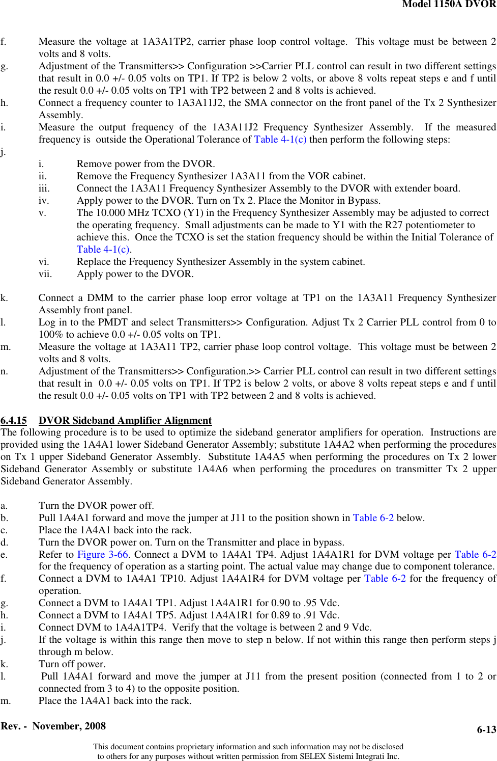


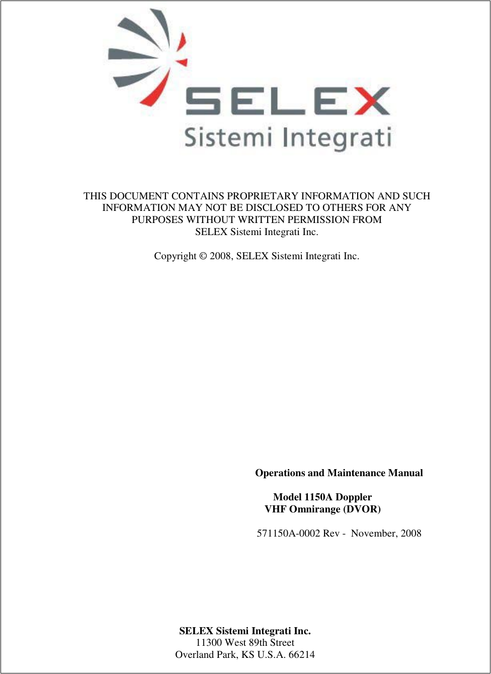
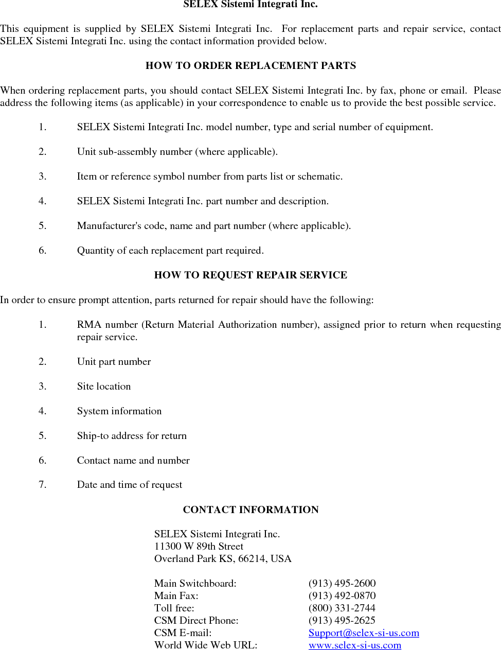
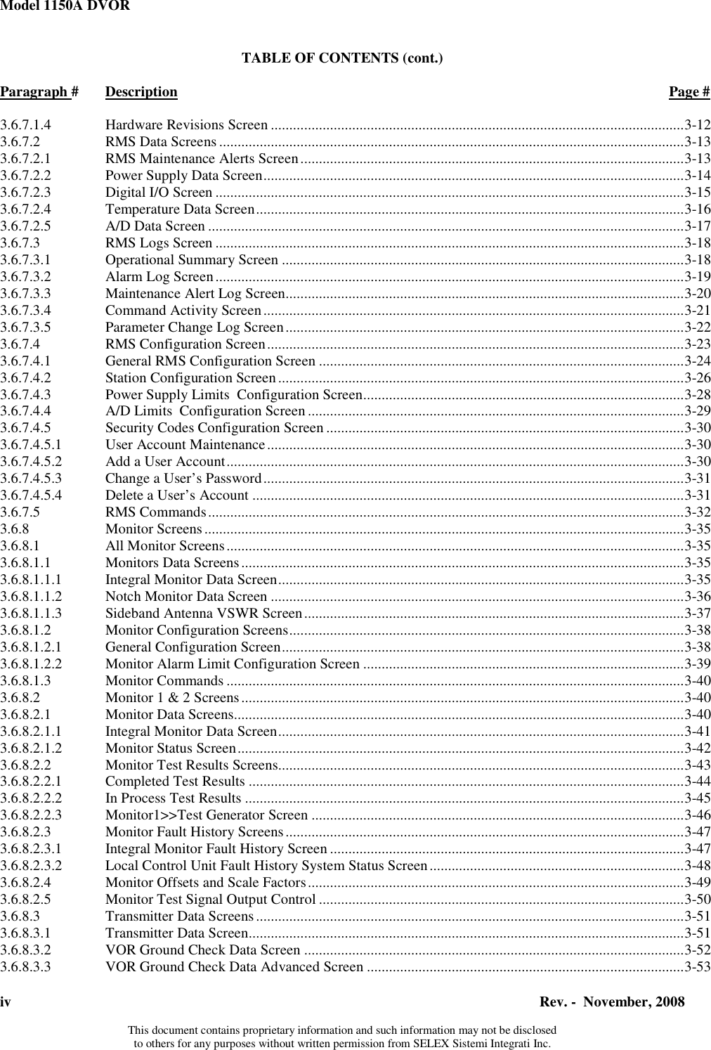
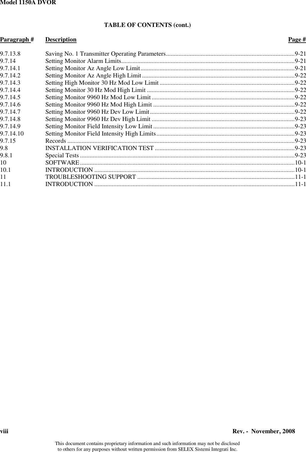
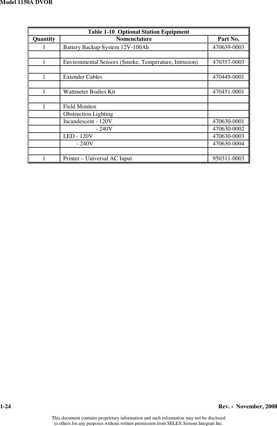
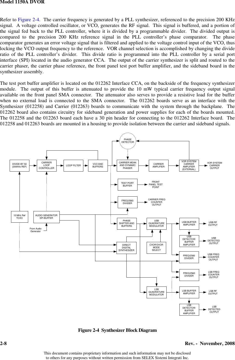
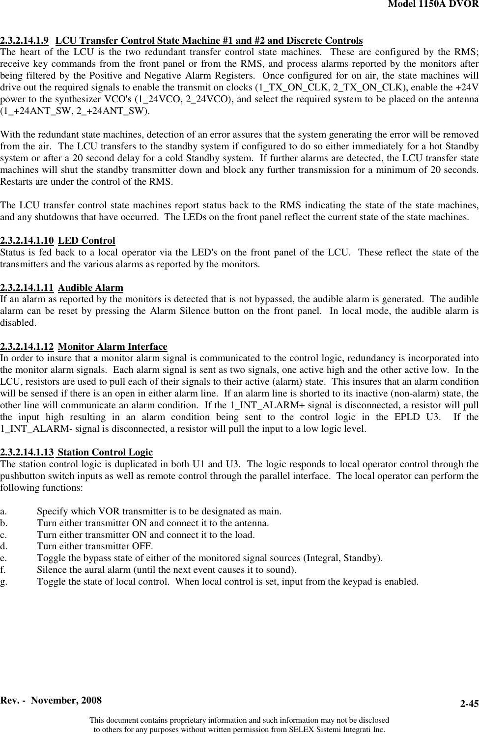
![Model 1150A DVOR Rev. - November, 2008 This document contains proprietary information and such information may not be disclosed to others for any purposes without written permission from SELEX Sistemi Integrati Inc. 9-19Figure 9-8 Sideband Phasing Diagram NOTE Bottom peaks within 5% of ground reference considered within tolerance. 9.7.13 Setting Transmitter Operating ParametersBefore the carrier forward power, carrier VSWR, SBO forward powers, and SBO VSWRs can be calibrated it will be necessary to check/set Transmitter No. 1 and No. 2’s operating parameters. 9.7.13.1 Setting Transmitter Ident CodeType RMS>>Configuration>>then enter Transmitter 1’s ident, then press [enter]. Transmitter No. 1’s new station’s code will be entered into the station's temporary memory. NOTE The system will accept from 2 to 4 alpha or numeric characters for the ident code. 9.7.13.2 Setting Transmitter Voice ModulationThe Voice modulation is normally set to 0% when an external voice source is not connected. When a voice system such as automated weather data is connected then select Transmitters>>Configuration>>Nominal. Enter the voice modulation from 0% to 30%, then press [enter]. The new voice modulation will be entered into the station’s temporary memory. Select Transmitters>>Configuration>> Offsets and Scale Factors. Set the Voice Modulation Scale for a value of 100% for both Tx #1 and Tx #2. 9.7.13.3 Setting Transmitter Ident Modulationa. Place Transmitter 1 on the antenna by pressing the Main #1 button on the LCU or PMDT. b. Select Transmitters>>Configuration>>Nominal. Enter the identification modulation 8%, then press [F7]. The new ident modulation will be entered into the station’s temporary memory. c. Select Transmitters>>Configuration>>Offsets and Scale Factors. For the Tx #1 Ident Modulation Scale for Ident Modulation, enter a value from 0 to 200% to adjust the value entered into the Nominal setting to the correct value as determined by the viewing Monitors>>Data screen. d. Place Transmitter 2 on the antenna by pressing the Main #2 button on the LCU or PMDT.](https://usermanual.wiki/Selex-Sistemi-Integrati/VOR2/User-Guide-1103052-Page-245.png)
![Model 1150A DVOR 9-20 Rev. - November, 2008 This document contains proprietary information and such information may not be disclosed to others for any purposes without written permission from SELEX Sistemi Integrati Inc. e. Select Transmitters>>Configuration>>Offsets and Scale Factors. For the Tx #2 Ident Modulation Scale for Ident Modulation, enter a value from 0 to 200% to adjust the value entered into the Nominal setting to the correct value as determined by the viewing Monitors>>Data screen. NOTE Typical setting for ident modulation is 8.0% but may be adjusted according to local requirements. 9.7.13.4 Setting Transmitter Reference Modulationa. Place Transmitter 1 on the antenna by pressing the Main #1 button on the LCU or PMDT. b. Select Transmitters>>Configuration>>Nominal. Enter the Reference modulation to 30%, then press [F7]. The new Reference modulation will be entered into the station’s temporary memory. c. Select Transmitters>>Configuration>>Offsets and Scale Factors. For the Tx #1 Reference Modulation Scale for Reference Modulation, enter a value from 0 to 200% to adjust the value entered into the Nominal setting to the correct value as determined by the viewing Monitors>>Data screen. d. Place Transmitter 2 on the antenna by pressing the Main #2 button on the LCU or PMDT. e. Select Transmitters>>Configuration>>Offsets and Scale Factors. For the Tx #2 Reference Modulation Scale for Reference Modulation, enter a value from 0 to 200% to adjust the value entered into the Nominal setting to the correct value as determined by the viewing Monitors>>Data screen. NOTE This value may be changed during the flight calibration. Use the Transmitters>>Configuration>>Offsets and Scale Factors to make the required correction 9.7.13.5 Reference to Sideband Phasinga. Set TX1 and TX2 circuit breakers to the ON position. b. Place Transmitter 1 on the antenna by pressing the Main #1 button on the LCU or PMDT. c. Place the monitors in bypass. d. Connect oscilloscope to 1A4A3 J2. Note composite signal waveform. Connect the scope sync input to 1A4A3 J3 Sync output and trigger on the falling edge. e. Adjust oscilloscope so that the composite signal is a full 30 Hz waveform (33 ms). f. On the PMDT select Transmitters>>Configuration>>Offset and Scale Factors. g. Adjust Tx #1 Carrier to Sideband Phase Offset (Coarse) in 90 degree increments until the waveform on the scope and the Monitors>>Data 9960 AM level displayed by the Monitor reaches a maximum amplitude. h. Add or subtract degrees for the Carrier Sideband Phase Offset (fine) until Monitors>>Data 9960 AM level displayed by the Monitor reaches maximum amplitude. i. Place Transmitter 2 on the antenna by pressing the Main #1 button on the LCU or PMDT. j. On the PMDT select Transmitters>>Configuration>>Offset and Scale Factors. k. Adjust Tx #2 Carrier to Sideband Phase Offset (Coarse) in 90 degree increments until the waveform on the scope and the Monitors>>Data 9960 AM level displayed by the Monitor reaches maximum amplitude. l. Add or subtract degrees for the Tx #2 Carrier Sideband Phase Offset (fine) until the Monitors>>Data 9960 AM level displayed by the Monitor reaches maximum amplitude. m. Once the reference to sideband phasing values have been established save the operating parameters. n. Switch transmitters so that Transmitter No. 1 is now operating normally. NOTE Further minor adjustments to the reference to sideband phasing may be made during commissioning flight check. This phase adjustment may increase the 9960 AM level as determined by the flight check panel technician. If during flight check the 9960 modulation is less than 30 percent the Reference-Sideband Phasing Parameter should be adjusted slightly to find the peak reading as determined by the panel technician. This will provide better sideband efficiency than by increasing the sideband power higher.](https://usermanual.wiki/Selex-Sistemi-Integrati/VOR2/User-Guide-1103052-Page-246.png)
![Model 1150A DVOR Rev. - November, 2008 This document contains proprietary information and such information may not be disclosed to others for any purposes without written permission from SELEX Sistemi Integrati Inc. 9-219.7.13.6 Setting Transmitter SBO Modulationa. Set TX1 and TX2 circuit breakers to the ON position. b. Place Transmitter 1 on the antenna by pressing the Main #1 button on the LCU or PMDT. c. Place the monitors in bypass. d. Select Monitors>>Data and view the 9960 Modulation level. e. Adjust Transmitters>>Configuration>>Offset and Scale Factors>> Tx Sideband RF Level Scale for Tx #1 so that Monitors>>Data 9960 Modulation level is 30%. f. Place Transmitter 2 on the antenna by pressing the Main #2 button on the LCU or PMDT. g. Adjust Transmitters>>Configuration>>Offset and Scale Factors>> Tx Sideband RF Level Scale for Tx #2 so that Monitors>>Data 9960 Modulation level is 30%. 9.7.13.7 Setting Transmitter Azimuth (Az) Indexa. Place Transmitter 1 on the antenna by pressing the Main #1 button on the LCU or PMDT. b. Select Transmitters>>Configuration>>Nominal. Set the Azimuth Index to 0.00 degrees. c. Select Transmitters>>Configuration>>Offsets and Scale Factors. In the Tx #1 Azimuth Angle Offset enter the Az offset from -20.00 to +20.00 as needed so that the field monitor reading matches the expected result from survey information. For example if the field monitor location was surveyed to be at 30 degrees then the monitor should read 30 degrees. After a new Az offset is entered then press [F7]. Transmitter No. 1’s new Az index will be entered into the station’s temporary memory. d. Place Transmitter 2 on the antenna by pressing the Main #2 button on the LCU or PMDT. e. Select Transmitters>>Configuration>>Offsets and Scale Factors. In the Tx #2 Azimuth Angle Offset enter the Az offset from -20.00 to +20.00 as needed so that the field monitor reading matches the expected result from survey information. For example if the field monitor location was surveyed to be at 30 degrees then the monitor should read 30 degrees. After a new Az offset is entered then press [F7]. Transmitter No. 2’s new Az index will be entered into the station’s temporary memory. NOTE AZ index is used to rotate the RF signal pattern so that the Monitor reading for the field monitor antenna matches the surveyed location for the antenna. During commissioning flight inspection corrections will be made to each transmitter to match the position determined by the flight inspection system. 9.7.13.8 Saving No. 1 Transmitter Operating Parametersa. Select RMS>>Config Backup and then press [enter]. This will place the Transmitter’s new operating parameters into electrically erasable memory. By means of the lithium battery, The Transmitter’s operating parameters are preserved in static ram if system power is lost. The electrically erasable memory is an added precaution against the loss of setup parameters. b. Apermanent copy should be placed onto the PMDT file system. Select System>>Configuration Save. You will be prompted for a file name. It is suggested that the configuration is saved into different files depicting progress up through the commissioning with different file names for each. 9.7.14 Setting Monitor Alarm LimitsOnce Transmitter No.1’s operating parameters have been set it will be necessary to check/set the Monitor alarm limits. Refer to Section 4 for appropriate limits. 9.7.14.1 Setting Monitor Az Angle Low Limita. Select Monitors>>Configuration>>Alarm Limits. The Alarm and Prealarm limits will be displayed for Monitor 1 and Monitor 2. b. Enter the Az Angle Low Alarm Limit that is needed, then press [F7]. Monitor No. 1’s new Az Angle Low Limit will be entered into the station’s temporary memory.](https://usermanual.wiki/Selex-Sistemi-Integrati/VOR2/User-Guide-1103052-Page-247.png)
![Model 1150A DVOR 9-22 Rev. - November, 2008 This document contains proprietary information and such information may not be disclosed to others for any purposes without written permission from SELEX Sistemi Integrati Inc. c. Enter the Az Angle Low PreAlarm Limit that is needed, then press [F7]. Monitor No 1 and 2’s new Az Angle Low PreAlarm Limit will be entered into the station’s temporary memory. 9.7.14.2 Setting Monitor Az Angle High Limita. Select Monitors>>Configuration>>Alarm Limits. The Alarm and Prealarm limits will be displayed for Monitor 1 and Monitor 2. b. Enter the az angle high alarm limit that is needed, then press [F7]. c. Enter the az angle high prealarm limit that is needed, then press [F7]. Monitor No. 1’s new az angle low prealarm limit will be entered into the station’s temporary memory. 9.7.14.3 Setting High Monitor 30 Hz Mod Low Limita. Select Monitors>>Configuration>>Alarm Limits. The Alarm and Prealarm limits will be displayed for Monitor 1 and Monitor 2. b. Enter the 30 Hz Mod low alarm limit that is needed, then press [F7]. Monitor No. 1 and 2’s 30 Hz Mod low limit will be entered into the station’s temporary memory. c. Enter the 30 Hz Mod low prealarm limit that is needed, then press [F7]. Monitor No. 1 and 2’s new 30 Hz Mod low prealarm limit will be entered into the station’s temporary memory. 9.7.14.4 Setting Monitor 30 Hz Mod High Limita. Select Monitors>>Configuration>>Alarm Limits. The Alarm and Prealarm limits will be displayed for Monitor 1 and Monitor 2. b. Enter the 30 Hz Mod high alarm limit that is needed, then press [F7]. Monitor No. 1 and 2’s new 30 Hz Mod high limit will be entered into the station’s temporary memory. c. Enter the 30 Hz Mod high prealarm limit that is needed then press [F7]. Monitor No. 1 and 2’s new 30 Hz Mod high prealarm limit will be entered into the station’s temporary memory. 9.7.14.5 Setting Monitor 9960 Hz Mod Low Limita. Select Monitors>>Configuration>>Alarm Limits. The Alarm and Prealarm limits will be displayed for Monitor 1 and Monitor 2. b. Enter the 9960 Hz Mod low alarm limit that is needed, then press [F7]. Monitor No. 1 and 2’s new 9960 Hz Mod low limit will be entered into the station’s temporary memory. c. Enter the 9960 Hz Mod low prealarm limit that is needed, then press [F7]. Monitor No. 1 and 2’s new 9960 Hz Mod low prealarm limit will be entered into the station’s temporary memory. 9.7.14.6 Setting Monitor 9960 Hz Mod High Limita. Select Monitors>>Configuration>>Alarm Limits. The Alarm and Prealarm limits will be displayed for Monitor 1 and Monitor 2. b. Enter the 9960 Hz Mod high alarm limit that is needed, then press [F7]. Monitor No. 1 and 2’s new 9960 Hz Mod high limit will be entered into the station’s temporary memory. c. Enter the 9960 Hz Mod high prealarm limit that is needed, then press [F7]. Monitor No. 1 and 2’s new 9960 Hz Mod high prealarm limit will be entered into the station’s temporary memory. 9.7.14.7 Setting Monitor 9960 Hz Dev Low Limita. Select Monitors>>Configuration>>Alarm Limits. The Alarm and Prealarm limits will be displayed for Monitor 1 and Monitor 2. b. Enter the 9960 Hz Dev low alarm limit that is needed, then press [F7]. Monitor No. 1 and 2’s new 9960 Hz Dev low limit will be entered into the station’s temporary memory. c. Enter the 9960 Hz Dev low prealarm limit that is needed, then press [F7]. Monitor No. 1 and 2’s new 9960 Hz Dev low prealarm limit will be entered into the station’s temporary memory.](https://usermanual.wiki/Selex-Sistemi-Integrati/VOR2/User-Guide-1103052-Page-248.png)
![Model 1150A DVOR Rev. - November, 2008 This document contains proprietary information and such information may not be disclosed to others for any purposes without written permission from SELEX Sistemi Integrati Inc. 9-239.7.14.8 Setting Monitor 9960 Hz Dev High Limitd. Select Monitors>>Configuration>>Alarm Limits. The Alarm and Prealarm limits will be displayed for Monitor 1 and Monitor 2. e. Enter the 9960 Hz Dev high alarm limit that is needed, then press [F7]. Monitor No. 1 and 2’s new 9960 Hz Dev high limit will be entered into the station’s temporary memory. f. Enter the 9960 Hz Dev high prealarm limit that is needed, then press [F7]. Monitor No. 1 and 2’s new 9960 Hz Dev high prealarm limit will be entered into the station’s temporary memory. 9.7.14.9 Setting Monitor Field Intensity Low Limita. Select Monitors>>Configuration>>Alarm Limits. The Alarm and Prealarm limits will be displayed for Monitor 1 and Monitor 2. b. Enter the Field Intensity Low Alarm Limit that is needed, then press [F7]. Monitor No. 1 and 2’s new Field Intensity Low Alarm Limit will be entered into the station’s temporary memory. c. Enter the Field Intensity Low PreAlarm Limit that is needed, then press [F7]. Monitor No. 1 and 2’s new Field Intensity Low PreAlarm limit will be entered into the station’s temporary memory. 9.7.14.10 Setting Monitor Field Intensity High Limitsa. Select Monitors>>Configuration>>Alarm Limits. The Alarm and Prealarm limits will be displayed for Monitor 1 and Monitor 2. b. Enter the Field Intensity High Alarm Limit that is needed, then press [F7]. Monitor No. 1 and 2’s new Field Intensity High Alarm Limit will be entered into the station’s temporary memory. c. Enter the Field Intensity High Alarm Limit that is needed, then press [F7]. Monitor No. 1 and 2’s new Field Intensity High PreAlarm Limit will be entered into the station’s temporary memory. 9.7.15 Recordsa. Select RMS>>Config Backup and then press [enter]. This will place the new operating parameters into electrically erasable memory. b. Apermanent copy should be placed onto the PMDT file system. Select System, Configuration Save. You will be prompted for a file name. It is suggested that the configuration is saved into different files depicting progress up through the commissioning with different file names for each. 9.8 INSTALLATION VERIFICATION TESTa. Check to make sure that all RF and power connections have been accomplished. b. If there are no further adjustments needed to be made to the antenna feed cables, fill the outside of the three conduits with putty to seal against water and vermin. c. Heat the shrink tubing on the 48 Sideband and 1 carrier antenna feed cables to provide a moisture seal on the cable connections. 9.8.1 Special TestsPerform verification procedures of Section 6.](https://usermanual.wiki/Selex-Sistemi-Integrati/VOR2/User-Guide-1103052-Page-249.png)