Sierra Wireless AR7584 Wireless Module User Manual Hardware Integration Guide
Sierra Wireless Inc. Wireless Module Hardware Integration Guide
UserManual.wiki
>
Sierra Wireless
>
AR7584 User Manual
AirPrime - AR7584 - Hardware Integration Guide
Navigation menu
Upload a User Manual
Namespaces
Wiki Guide
HTML
PDF
Info
Views
User Manual
Discussion / Help
Navigation
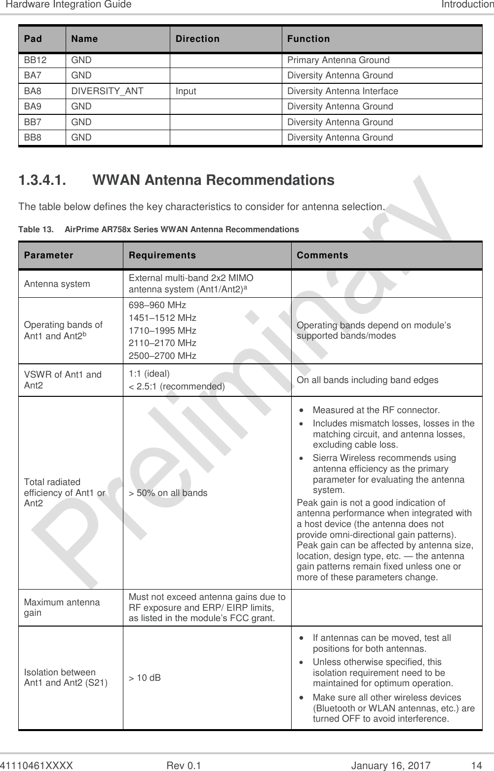
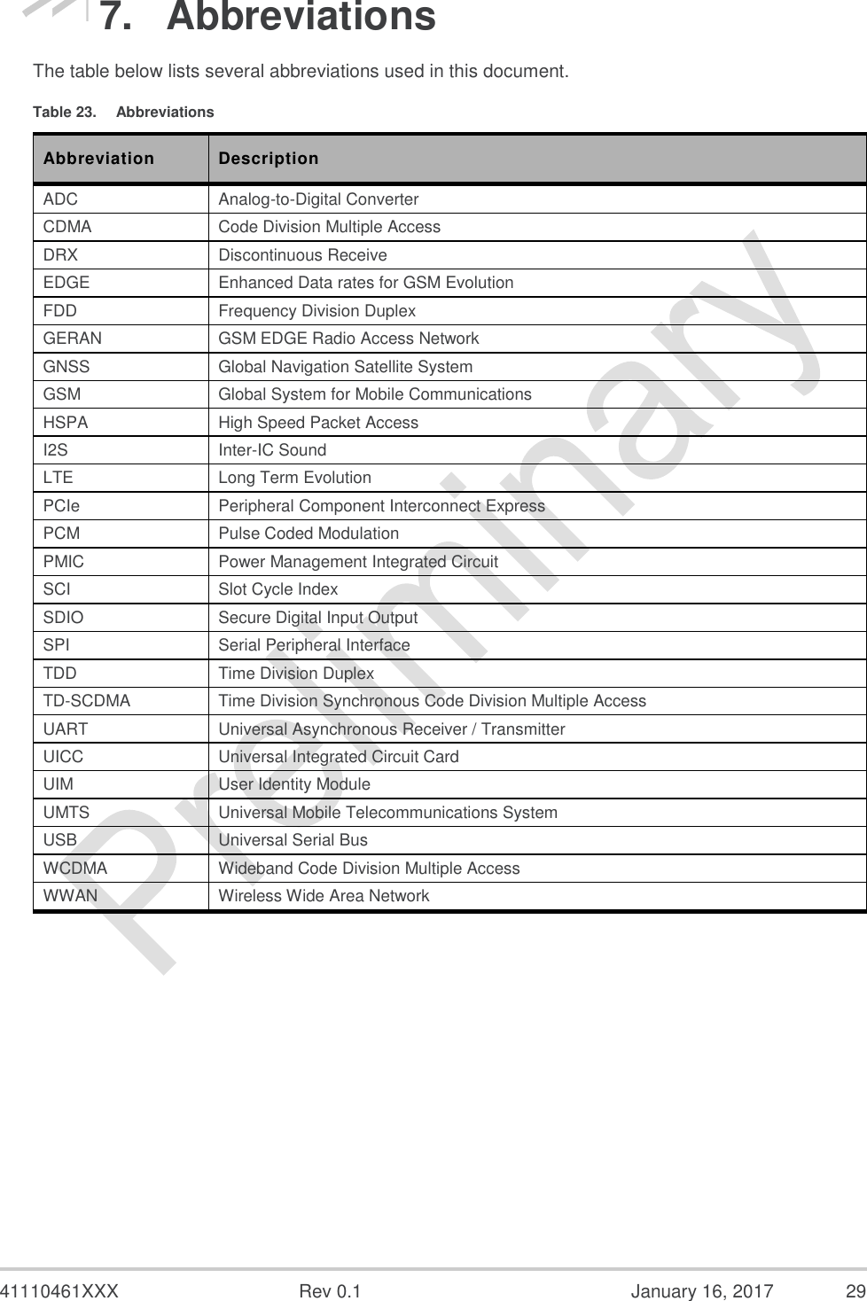
![41110461 Rev 0.1 January 16, 2017 25 4. Firmware and Tools The AirPrime AR7582 are designed based on Qualcomm’s MDM9628 chipset, which contains a Modem Processor for running modem firmware components and an Application Processor for running embedded Linux applications. Various tools are provided by Qualcomm and developed by Sierra Wireless for developing and commercializing the AirPrime AR7584. 4.1. Modem Firmware The MDM9628 Modem Process contains the following categories of firmware, with possible modifications/extensions by Sierra Wireless as indicated: LTE/ WCDMA/ TD-SCDMA air interface protocols GNSS engine IMS protocol stack AT Command Processor: New AT commands will be added by Sierra Wireless. See document [8] for the complete list of AT Commands for AR758x. Data services Drivers/ BSP: Some modifications will be made to ensure the firmware can communicate with the AR758x module hardware properly. UICC functions Memory Management: Built-in redundancy and continuous monitoring against memory corruption Antenna Protection Voice support 4.2. Tools The following tools will be needed for the AirPrime AR7584 development, testing and commercialization. Firmware Update Tool Linux driver and Application Downloader Logging Tool Qualcomm’s QXDM (license with Qualcomm required) Qualcomm’s QPST (license with Qualcomm required)](https://usermanual.wiki/Sierra-Wireless/AR7584/User-Guide-3651707-Page-25.png)
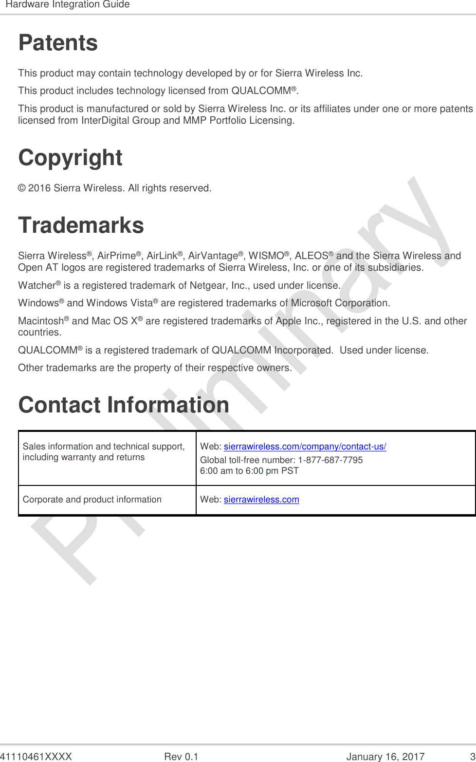
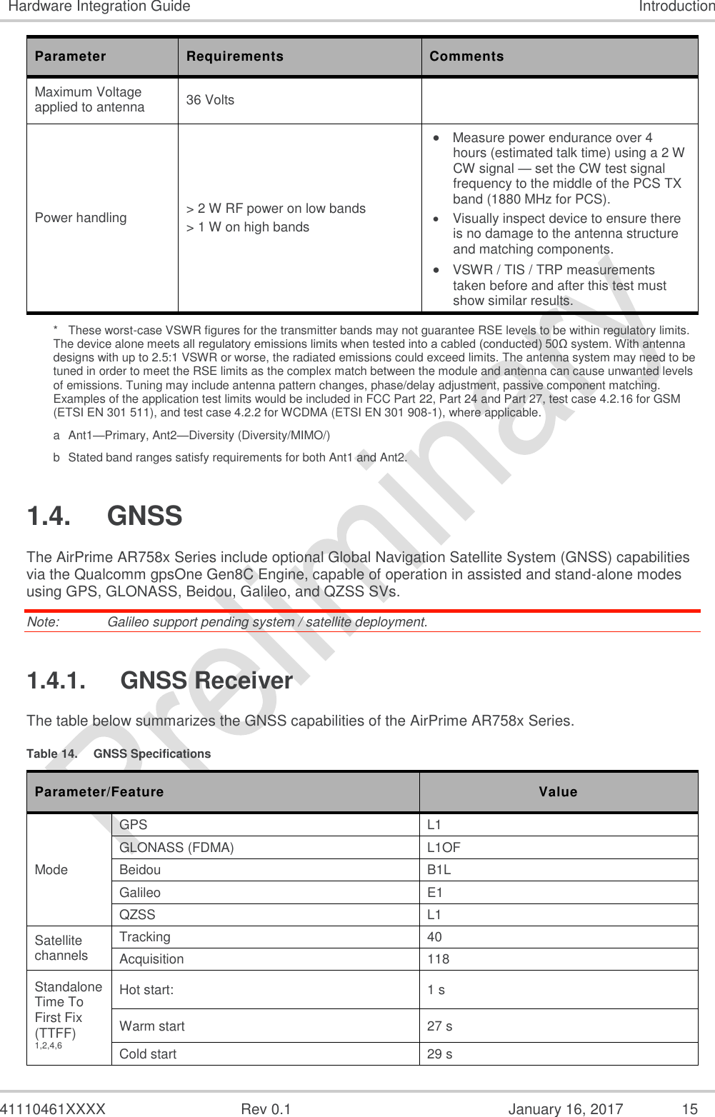
![41110461XXX Rev 0.1 January 16, 2017 28 6. References The table below lists the reference specifications for this product. Table 22. Reference Specifications Ref Title Rev Issuer [1] 3GPP TS 51.010-1 Version 7.3.1 3GPP [2] 3GPP TS 34.121-1 V8 3GPP [3] 3GPP TS 36.521-1 V9 3GPP [4] Universal Serial Bus Specification V2.0 USB Implementers Forum [5] Universal Serial Bus CDC Subclass Specification for Wireless Mobile Communication Devices V1.0 USB Implementers Forum [6] Universal Serial Bus Class Definitions for Communication Devices V1.1 USB Implementers Forum [7] AirPrime - AR7 Series - Customer Process Guidelines - Sierra Wireless [8] AirPrime - AR75xx - AT Command Interface Specification - 4112841 V1.5 Sierra Wireless [9] AirPrime AR7xxx Firmware Download Guide - Sierra Wireless [10] AirPrime AR758x Thermal Management Application Note - 2174114 V1.0 Sierra Wireless [11] AirPrime AR758x Current Consumption Application Note - 2174115 V1.0 Sierra Wireless [12] AirPrime - AR Series - Hardware Compatibility APN - 4116174 V0.8 Sierra Wireless [13] AirPrime - AR7552 - Hardware Integration Guide – 4117336 V1.0 Sierra Wireless](https://usermanual.wiki/Sierra-Wireless/AR7584/User-Guide-3651707-Page-28.png)