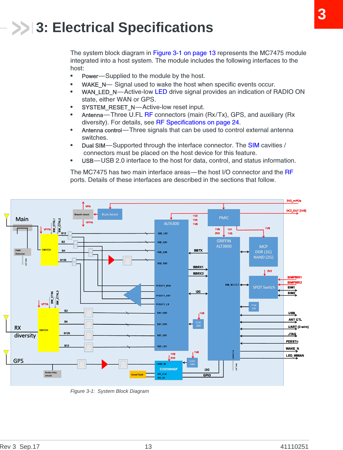
Sierra Wireless MC7475 Radio Module User Manual AirPrime MC7475 Product Technical Specification
Sierra Wireless Inc. Radio Module AirPrime MC7475 Product Technical Specification
Contents
- 1. MC7475 User Manual
- 2. MC7475 User Manual_r3
MC7475 User Manual_r3
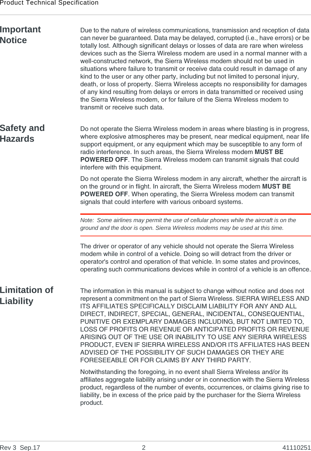
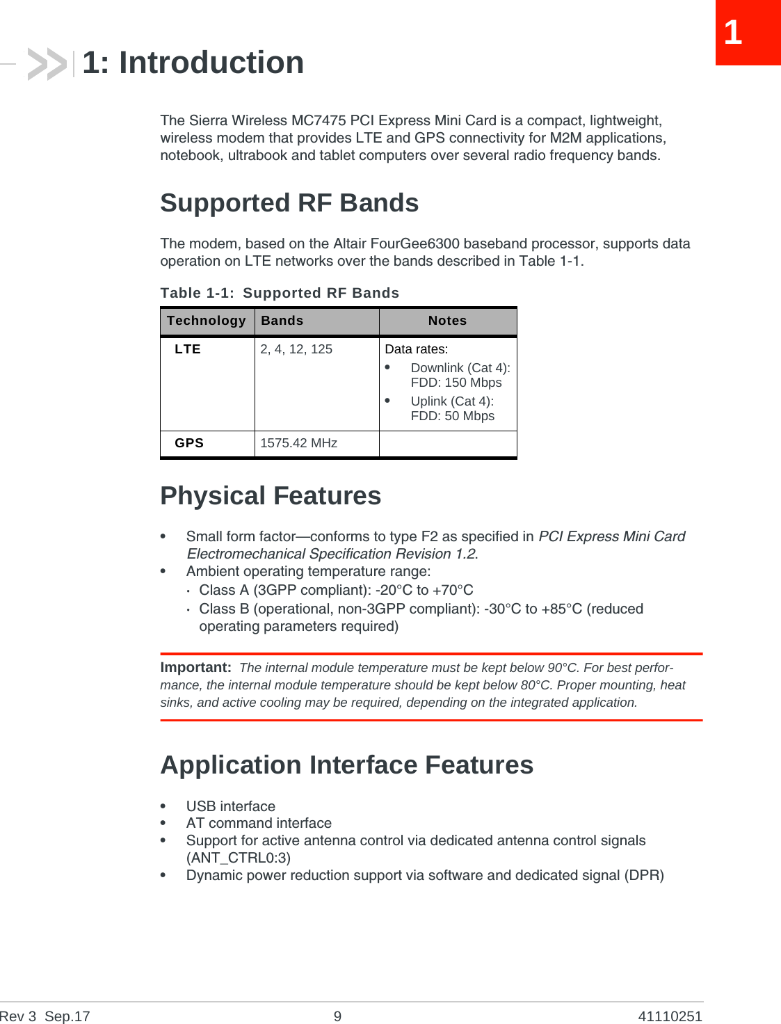
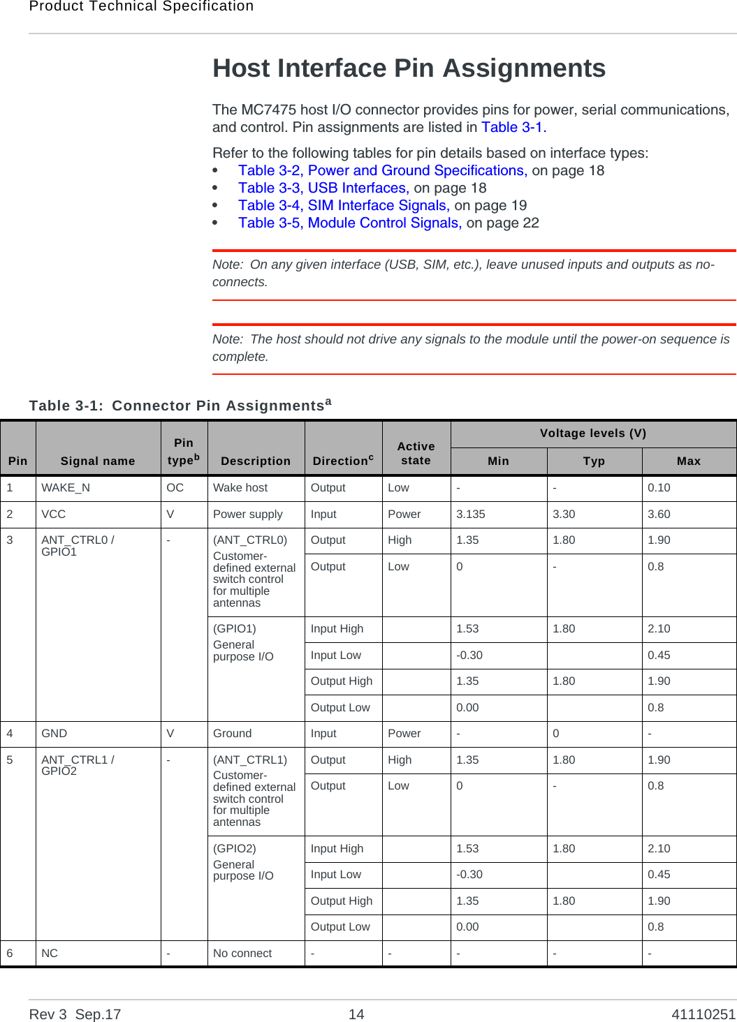
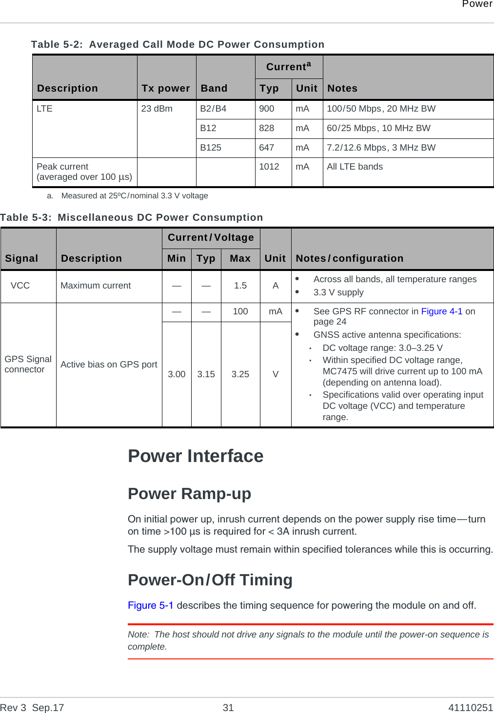
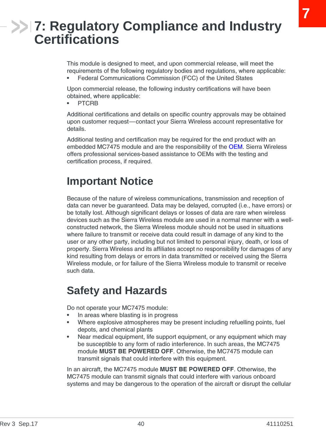
![Product Technical SpecificationRev 3 Sep.17 18 41110251Power SupplyThe host provides power to the MC7475 through multiple power and ground pins as summarized in Table 3-2.The host must provide safe and continuous power at all times; the module does not have an independent power supply, or protection circuits to guard against electrical issues.USB InterfaceImportant: Host support for USB 2.0 signals is required.The device supports a USB 2.0 interface for communication between the host and module.The interface complies with the [7] Universal Serial Bus Specification, Rev 2.0, and the host device must be designed to the same standards (subject to details shown in Table 3-3 below). (Note: When designing the host device, careful PCB layout practices must be followed.)USB Throughput PerformanceThis device has been designed to achieve optimal performance and maximum throughput using USB high-speed mode (USB 2.0). Although the device may operate with a high speed host, throughput performance will be on an “as is” e. The module must not be plugged into a port that supports PCI Express—the pin is used by a PCIE signal, which can cause the module to be in reset state or occasionally reset.f. Max voltage level when current < 100 mA.Table 3-2: Power and Ground SpecificationsName Pins Specification Min Typ Max UnitsVCC 2, 24, 39, 41, 52 Voltage range See Table 3-1 on page 14.Ripple voltage --100 mVppGND 4, 9, 15, 18, 21, 26, 27, 29, 34, 35, 37, 40, 43, 50- - 0 - VTable 3-3: USB InterfacesName Pin DescriptionUSB 2.0 USB_D- 36 USB data negativeUSB_D+ 38 USB data positive](https://usermanual.wiki/Sierra-Wireless/MC7475.MC7475-User-Manual-r3/User-Guide-3569786-Page-18.png)
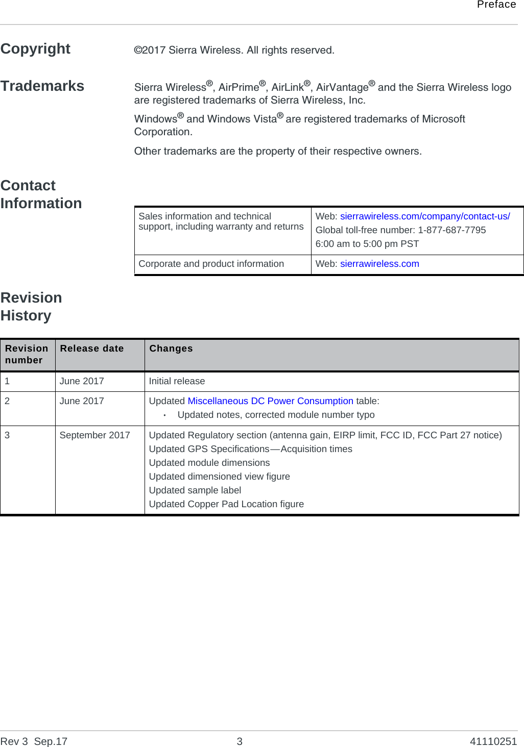
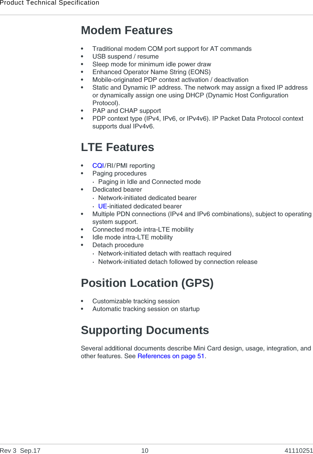
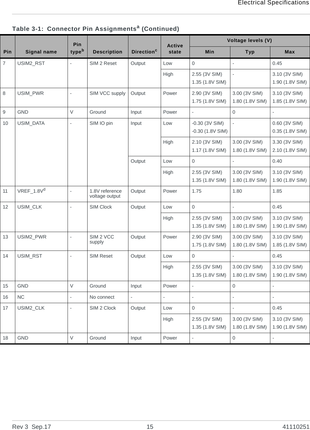
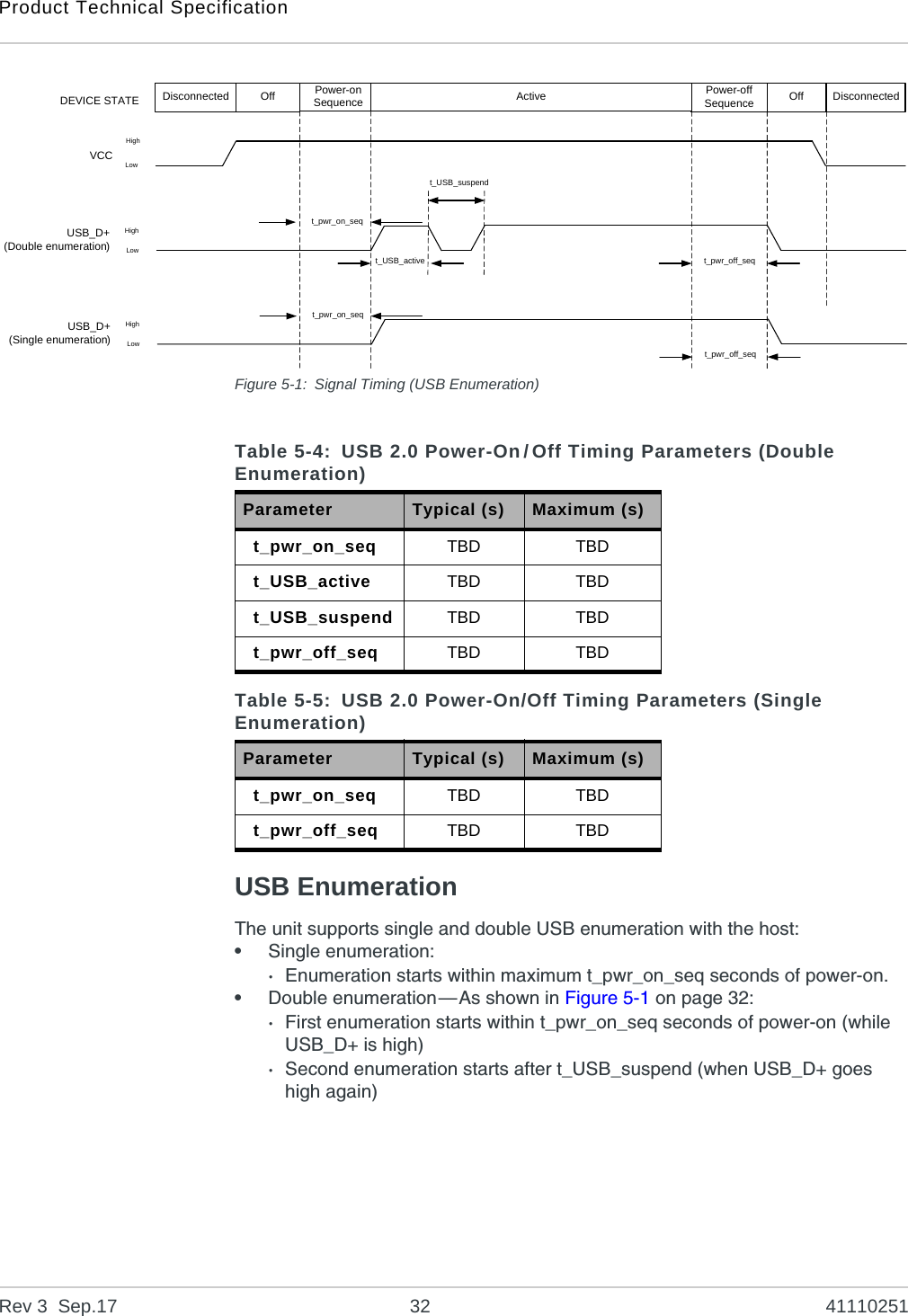
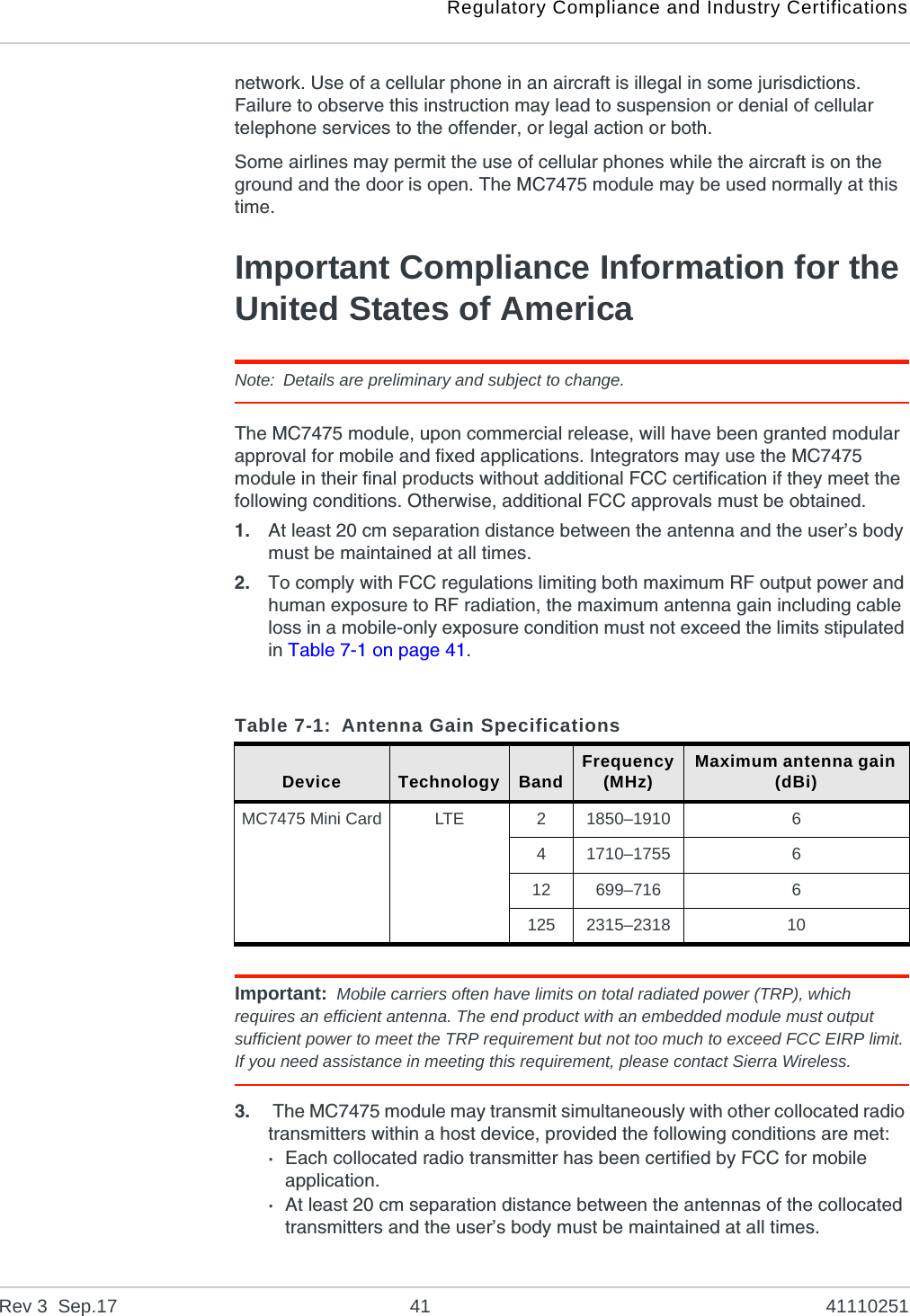
![Product Technical SpecificationRev 3 Sep.17 22 41110251Control Interface (Signals)The MC7475 provides signals for:•Waking the host when specific events occur•LED driver outputThese signals are summarized in Table 3-5 and paragraphs that follow.WAKE_N — Wake HostNote: Host support for WAKE_N is optional.The module uses WAKE_N to wake the host when specific events occur.The host must provide a 5 k–100 k pullup resistor that considers total line capacitance (including parasitic capacitance) such that when WAKE_N is deasserted, the line will rise to 3.3 V (Host power rail) in < 100 ns.See Figure 3-4 on page 22 for a recommended implementation.Figure 3-4: Recommended WAKE_N ConnectionWAN_LED_N—LED OutputNote: Host support for WAN_LED_N is optional.The module drives the LED output according to [6] PCI Express Mini Card Electromechanical Specification Revision 2.1.Note: The LED configuration is customizable. Contact your Sierra Wireless account repre-sentative for details.Table 3-5: Module Control SignalsName Pin Description Typeaa. OC—Open Collector; PU—Digital pin Input, internal pull upWAKE_N 1Wake host OCWAN_LED_N 42 LED driver OCControlRWAKE_N123Q5k-100kHostVCCMiniCard](https://usermanual.wiki/Sierra-Wireless/MC7475.MC7475-User-Manual-r3/User-Guide-3569786-Page-22.png)

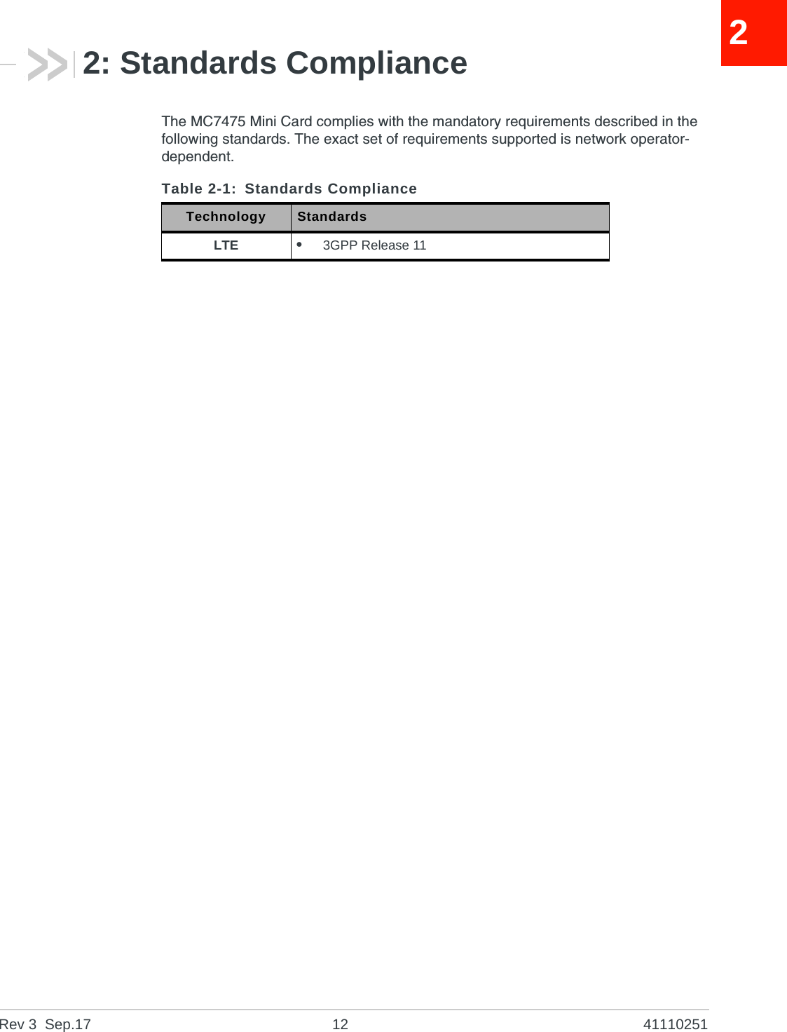
![Rev 3 Sep.17 51 411102511111: ReferencesThis guide deals specifically with hardware integration issues that are unique to AirPrime embedded modules.Sierra Wireless DocumentsFor additional documents describing embedded module design, usage, and integration issues, contact your Sierra Wireless account representative.Command Documents[1] AT Command Set for User Equipment (UE) (Release 6) (3GPP TS 27.007)Industry/Other DocumentsThe following non-Sierra Wireless references are not included in your documentation package:[2] FCC Regulations - Part 15 - Radio Frequency Devices[3] IEC-61000-4-2 level 3[4] IEC-61000-4-2 level (Electrostatic Discharge Immunity Test)[5] Mobile Station (MS) Conformance Specification; Part 4: Subscriber Interface Module (Doc# 3GPP TS 11.10-4)[6] PCI Express Mini Card Electromechanical Specification Revision 2.1[7] Universal Serial Bus Specification, Rev 2.0[8] JESD22-A114-B[9] JESD22-C101](https://usermanual.wiki/Sierra-Wireless/MC7475.MC7475-User-Manual-r3/User-Guide-3569786-Page-51.png)