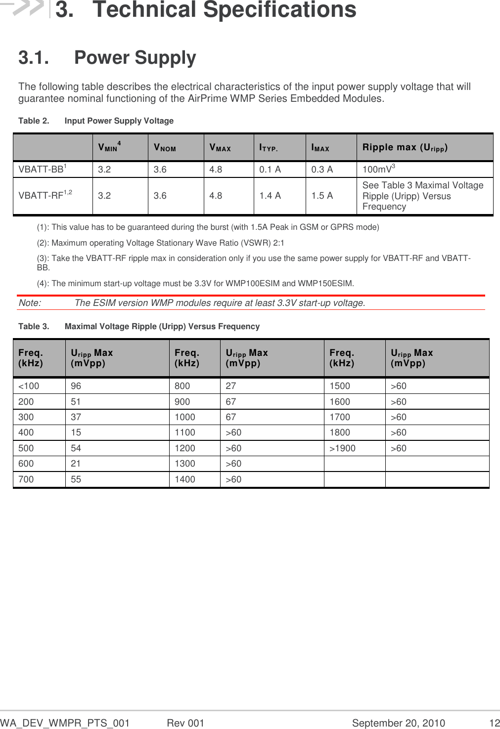
Sierra Wireless WMP100 GSM Module User Manual User Guide
Sierra Wireless Inc. GSM Module User Guide
UserManual.wiki
>
Sierra Wireless
>
WMP100 User Manual
>
User Guide
Contents
1.
User Manual
2.
User Guide
User Guide
Navigation menu
Upload a User Manual
Namespaces
Wiki Guide
HTML
PDF
Info
Views
User Manual
Discussion / Help
Navigation

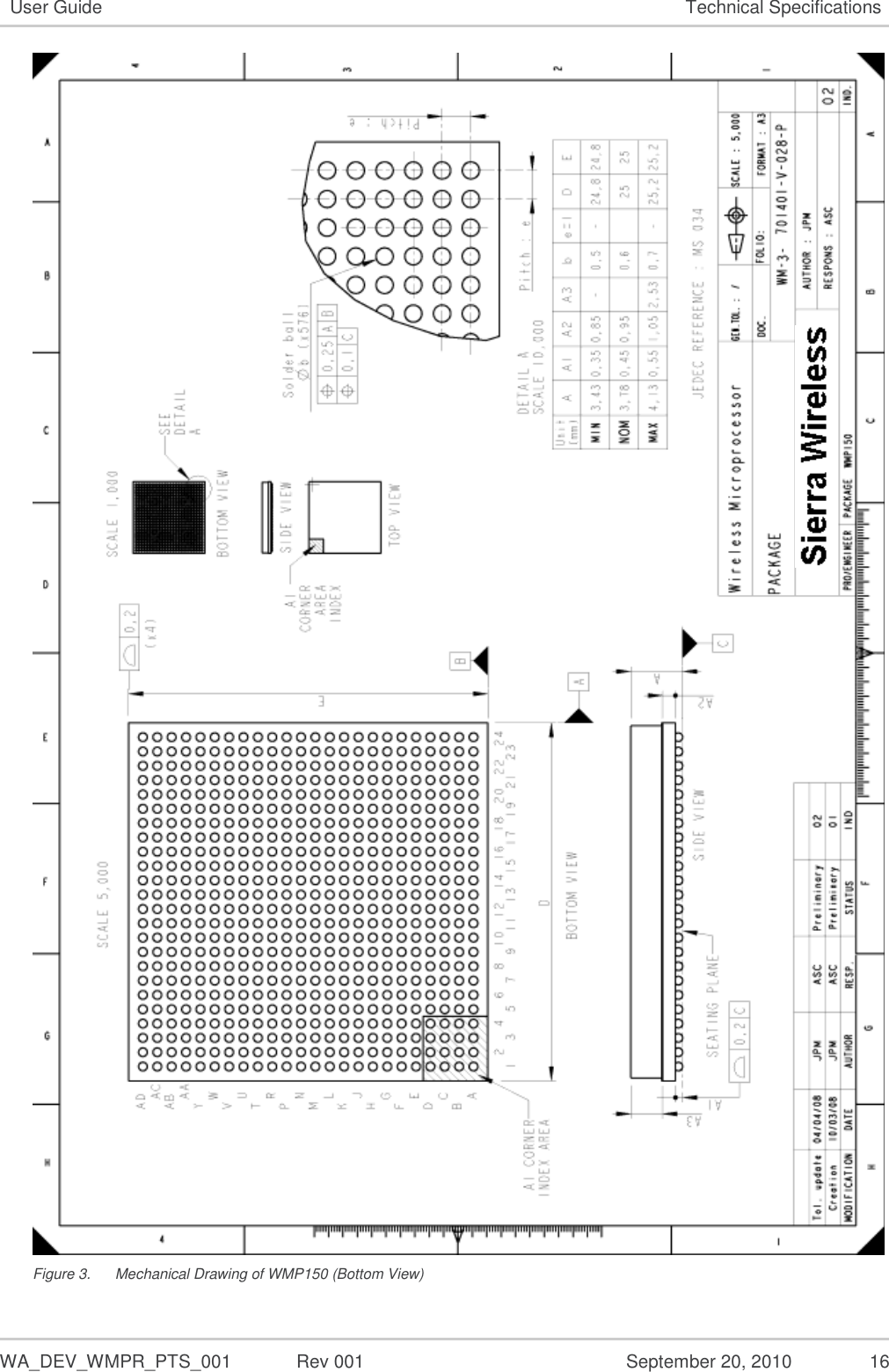

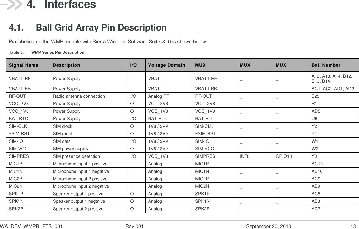
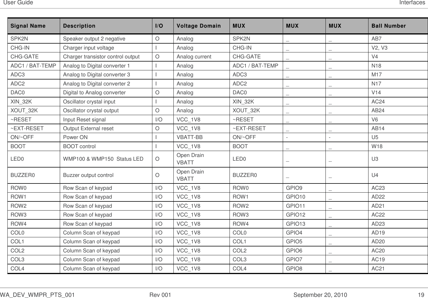
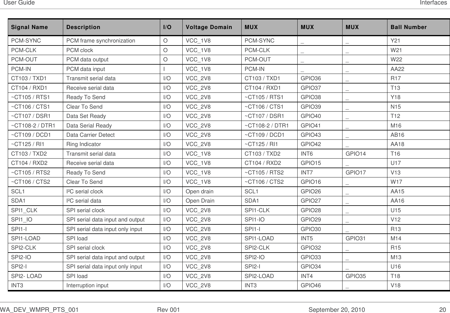
![WA_DEV_WMPR_PTS_001 Rev 001 September 20, 2010 29 User Guide References 6.2. Reference Documents For more details, several reference documents can be consulted. The Sierra Wireless documents referenced herein are provided in the Sierra Wireless documentation package; however, the general reference documents which are not Sierra Wireless owned are not provided in the documentation package. Check the Sierra Wireless website at http://sierrawireless.com for the latest documentation available. 6.2.1. Sierra Wireless Reference Documentation [1] AirPrime WMP100 & WMP150 Embedded Module Technical Specification Reference: WM_DEV_WMP150_PTS_002 [2] AirPrime WMP100 & WMP150 Embedded Module Development Kit User Guide Reference: WM_DEV_WMP150_UGD_001 [3] AT Command Interface Guide for Firmware v7.0 or later Reference: WM_DEV_OAT_UGD_079 [4] Manufacturing Guidelines Reference: WM_PGM_WUP_UGD_001 [5] DWLWin Download Application User Guide Reference: WM_DEV_TOO_UGD_010 [6] ADL User Guide for OS v6.00 or later Reference: WM_DEV_OAT_UGD_080 6.2.2. General Reference Documentation [7] “I2C Bus Specification”, Version 2.0, Philips Semiconductor 1998 [8] ISO 7816-3 Standard](https://usermanual.wiki/Sierra-Wireless/WMP100.User-Guide/User-Guide-1355016-Page-29.png)