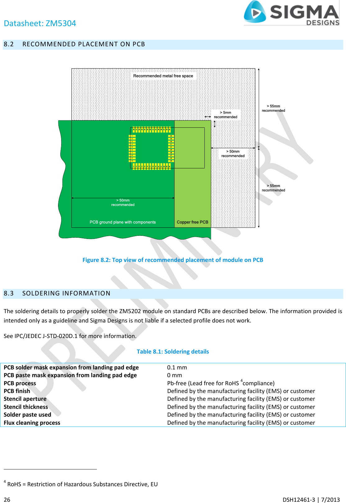
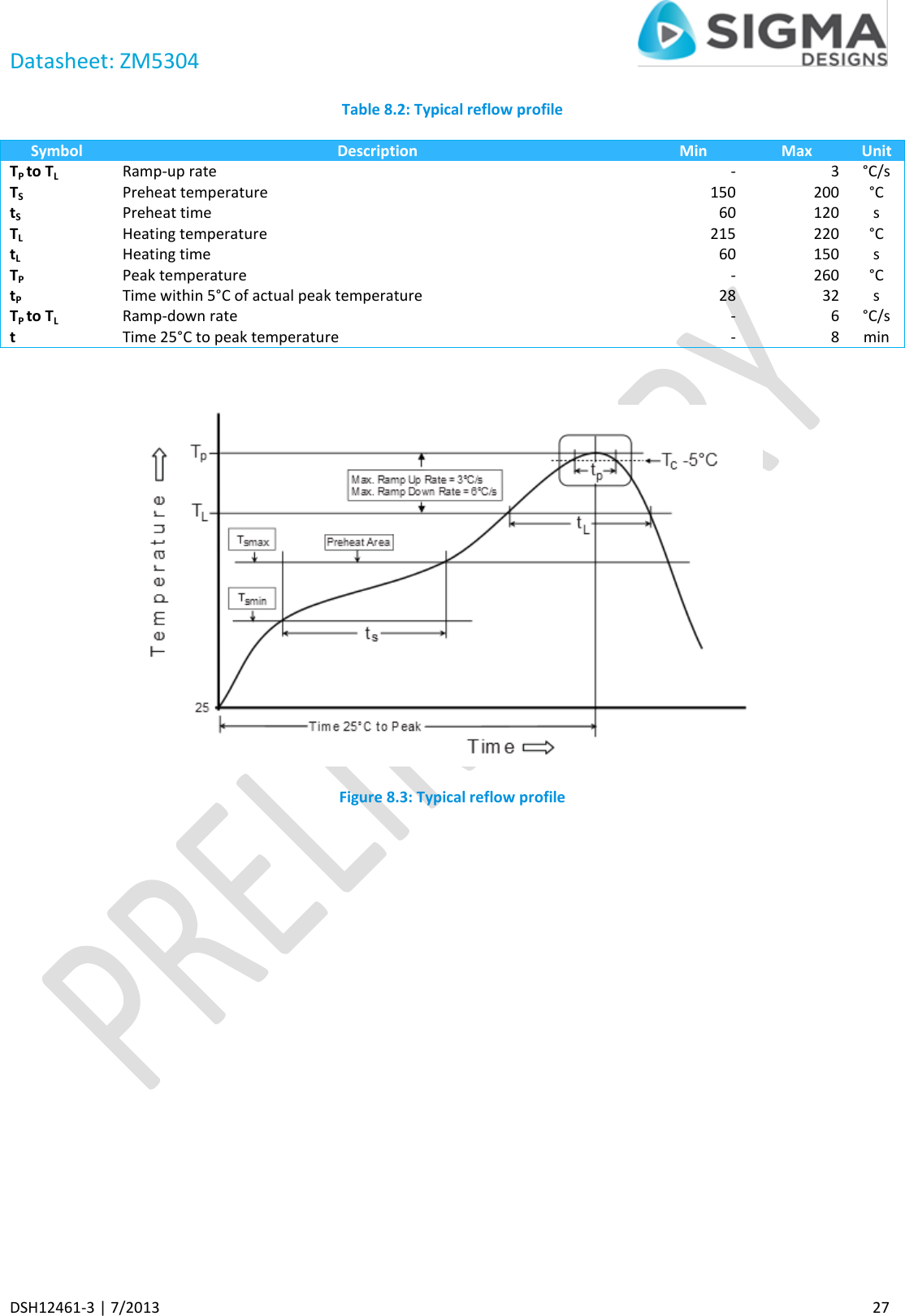
Sigma Designs ZM5304-U Z-Wave Serial Interface Module with On-Board Antenna User Manual
Sigma Designs Inc Z-Wave Serial Interface Module with On-Board Antenna
UserManual.wiki
>
Sigma Designs
>
ZM5304 U User Manual
User Manual.pdf
Navigation menu
Upload a User Manual
Namespaces
Wiki Guide
HTML
PDF
Info
Views
User Manual
Discussion / Help
Navigation
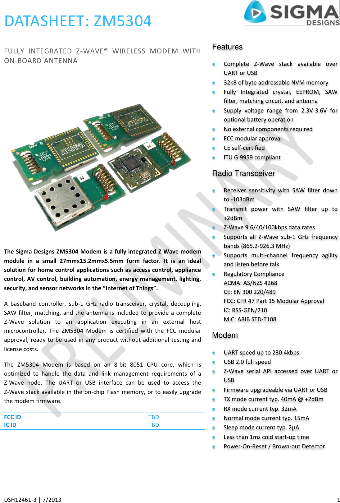
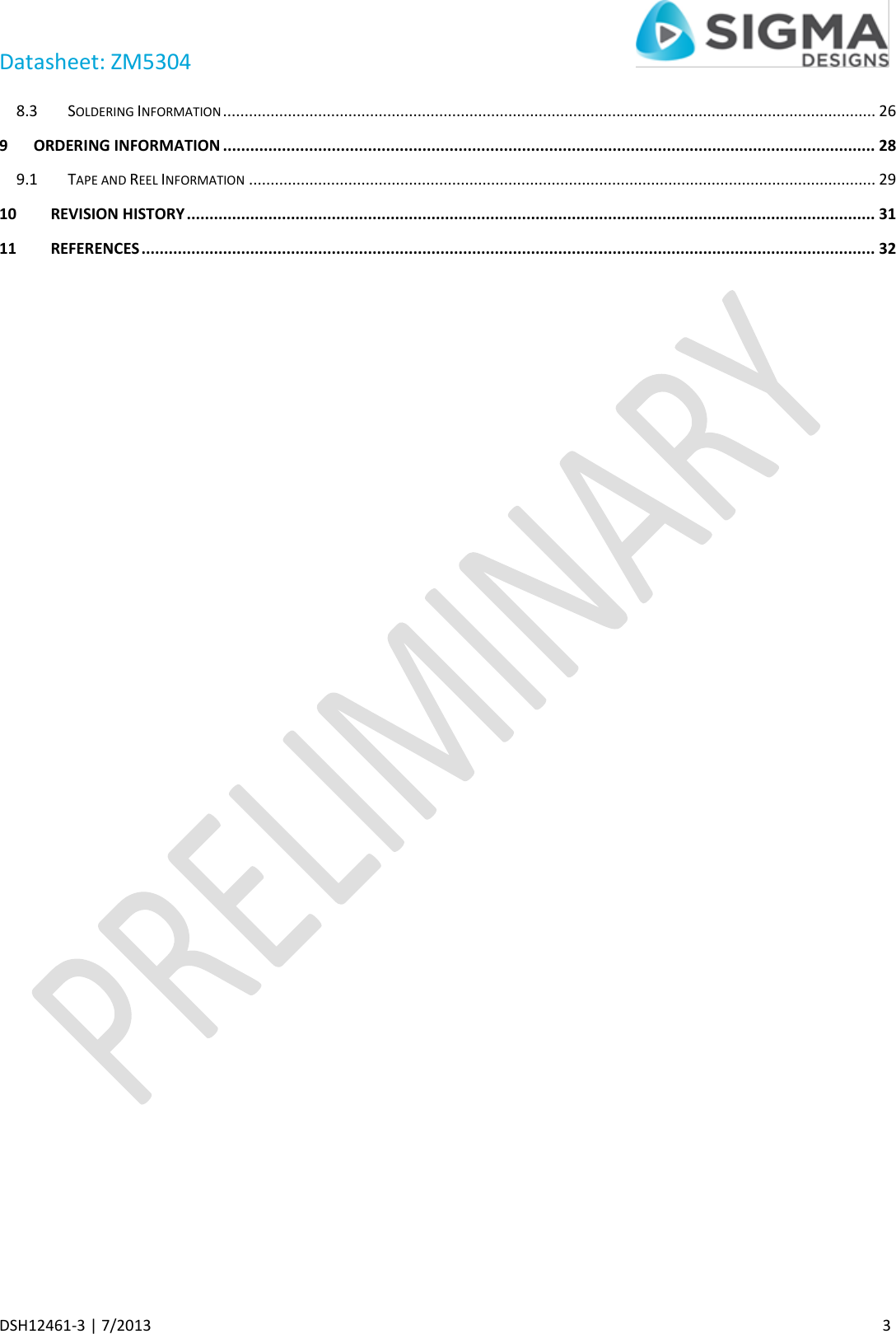
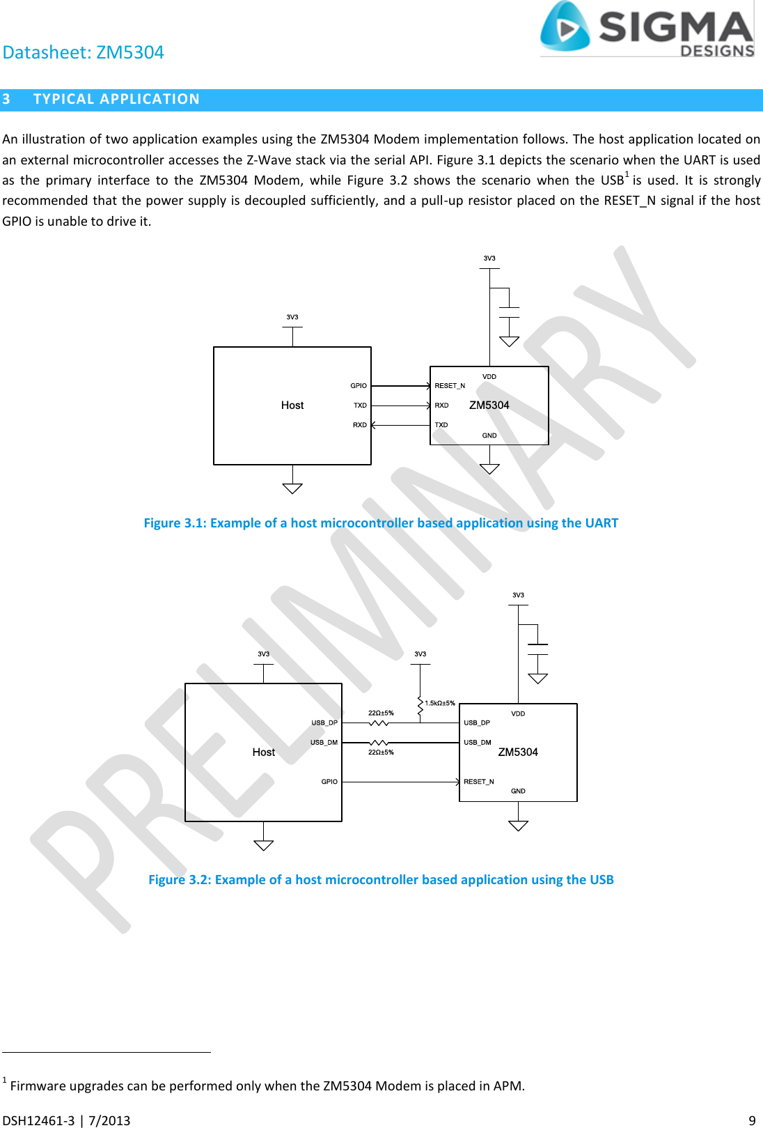
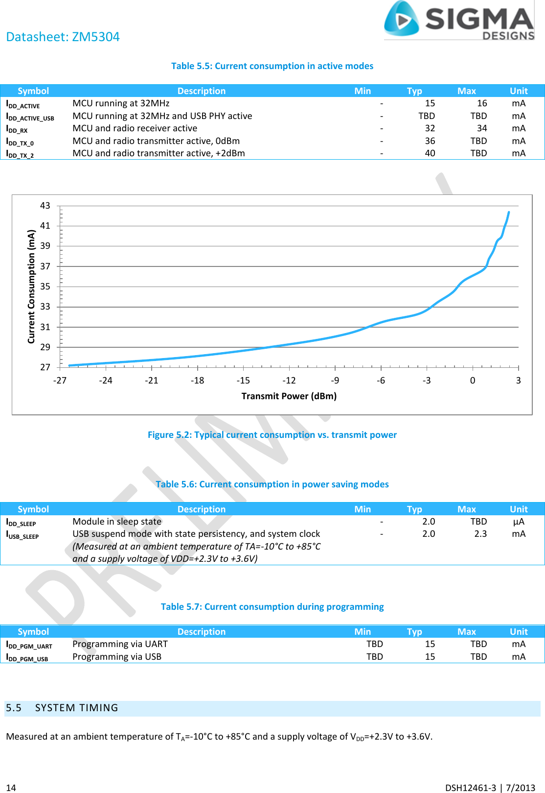
![Datasheet: ZM5304 DSH12461-3 | 7/2013 7 ZM5304USB_DPUSB_DMHost Figure 2.4: USB interface 2.1.9 WATCHDOG The watchdog helps prevents the CPU from entering a deadlock state. A timer that is enabled by default achieves this by triggering a reset event in case it overflows. The timer overflows in 1 second, therefore it is essential that the software clear the timer periodically. The watchdog is disabled when the chip is in power down mode, and automatically restarts with a cleared timer when waking up to the active mode. 2.1.10 WIRELESS TRANSCEIVER The wireless transceiver is a sub-1 GHz ISM narrowband FSK radio, a modem, and a baseband controller. This architecture provides an all-digital direct synthesis transmitter and a low IF digital receiver. The Z-Wave protocol currently utilizes 2-key FSK/GFSK modulation schemes at 9.6/40/100 kbps data rates throughout a span of carrier frequencies from 865.2 to 926.3MHz. The output power of the transmitter is configurable in the range -26dBm to +2dBm (VDD = 2.3 to 3.6V, TA = -10 to +85°C). 2.2 MEMORY MAP An application executing on an external host microcontroller can access a minimum of 16kB allocated on the higher address space of the integrated EEPROM via the serial API. As shown in Figure 2.5, the protocol data is stored in the lower address space. A serial API function returns the size of the application data space. [1][2] EEPROM Memory(Byte addressable)Protocol Data(Reserved for Modem)Application Data(Available to Host)016kB (min)Offset0 Figure 2.5: EEPROM memory map](https://usermanual.wiki/Sigma-Designs/ZM5304-U/User-Guide-2052478-Page-7.png)
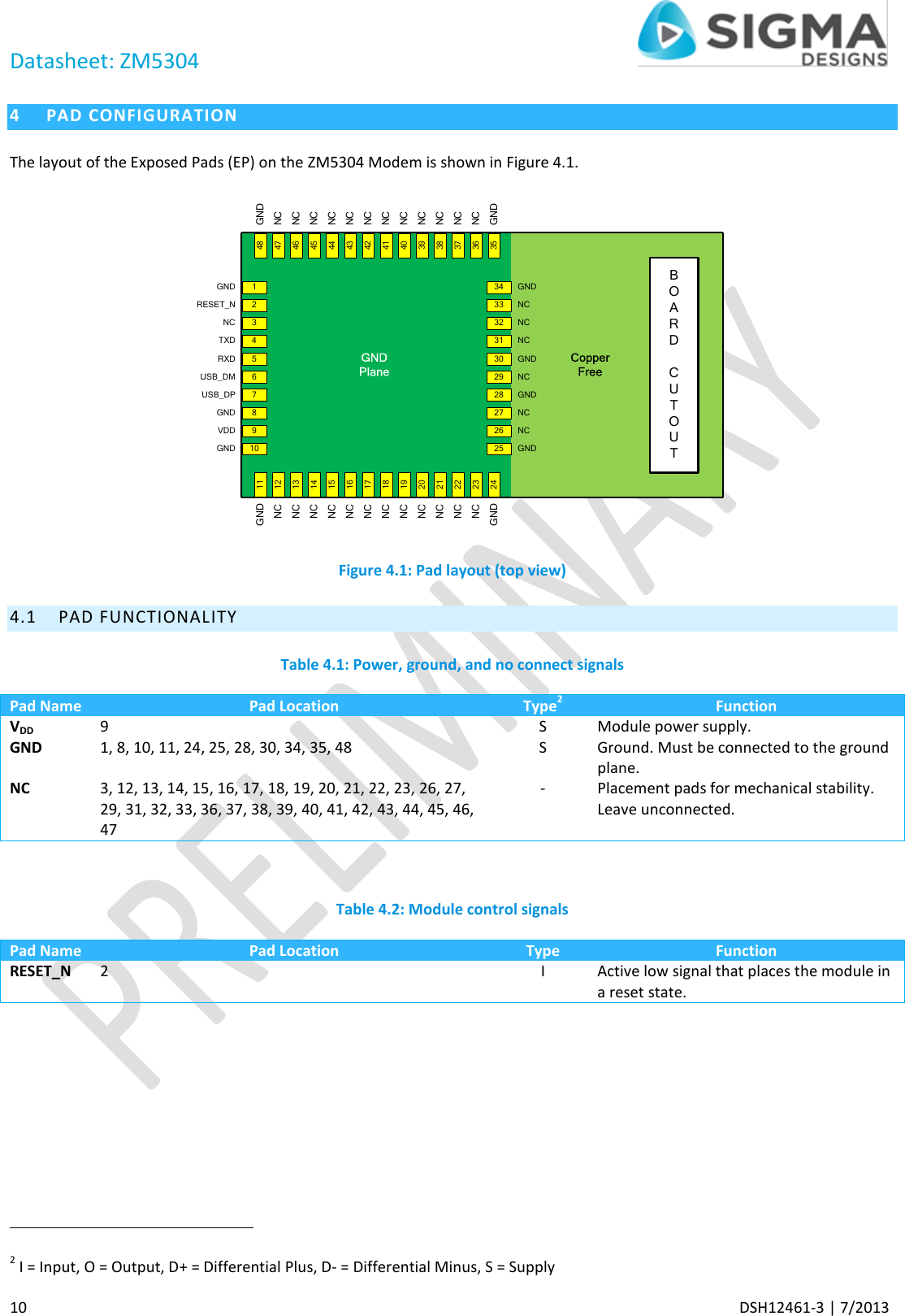
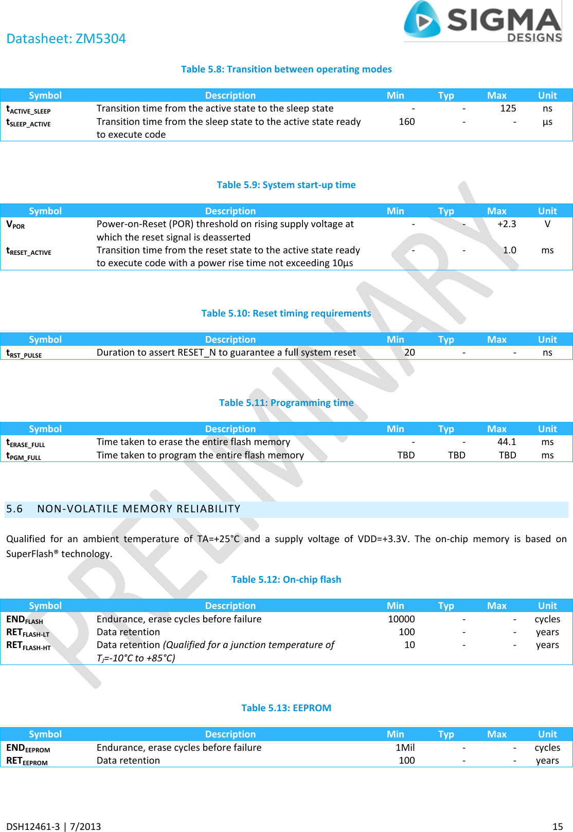
![Datasheet: ZM5304 8 DSH12461-3 | 7/2013 2.3 MODULE PROGRAMMING The firmware of the ZM5304 Modem can be upgraded through the UART or USB interface. [3] In-System Programming is the default mode delivered from the factory. 2.3.1 ENTERING IN-SYSTEM PROGRAMMING MODE The module can be placed into the UART In-System Programming (ISP) mode by asserting the active low RESET_N signal for 4.2ms. The programming unit of the module then waits for the “Interface Enable” serial command before activating the ISP mode over the UART. 2.3.2 ENTERING AUTO PROGRAMMING MODE Alternatively, the module can be placed into the Auto Programming Mode (APM) by calling a serial API function. The programming unit of the module will enter APM immediately after a hardware or software reset. Once the module is in APM, the firmware can be written to the internal flash using either the UART or USB interface. 2.4 POWER SUPPLY REGULATOR While the supply to the digital I/O circuits is unregulated, on-chip low-dropout regulators derive all the 1.5 V and 2.5 V internal supplies required by the Micro-Controller Unit (MCU) core logic, non-volatile data registers, flash, and the analogue circuitry.](https://usermanual.wiki/Sigma-Designs/ZM5304-U/User-Guide-2052478-Page-8.png)
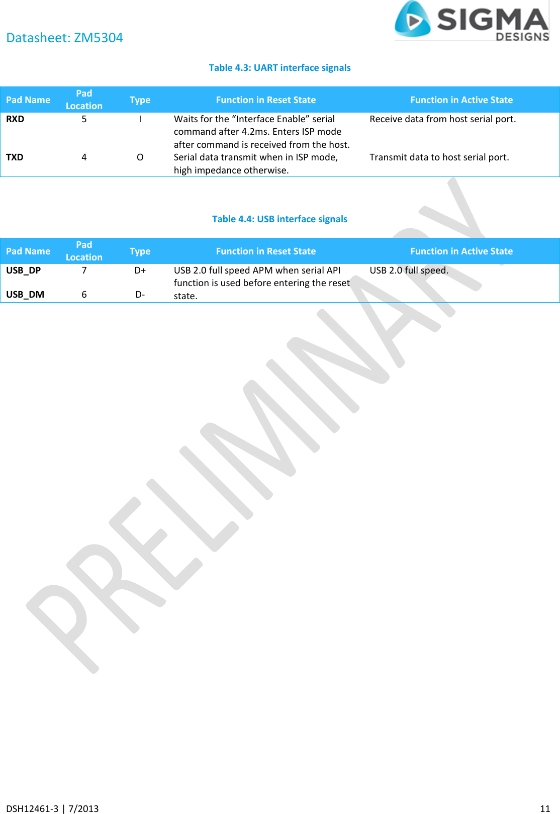
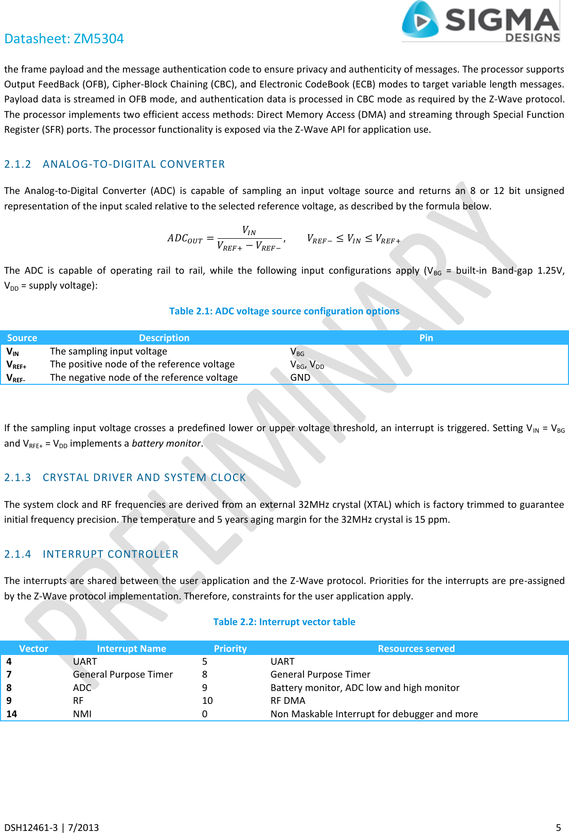
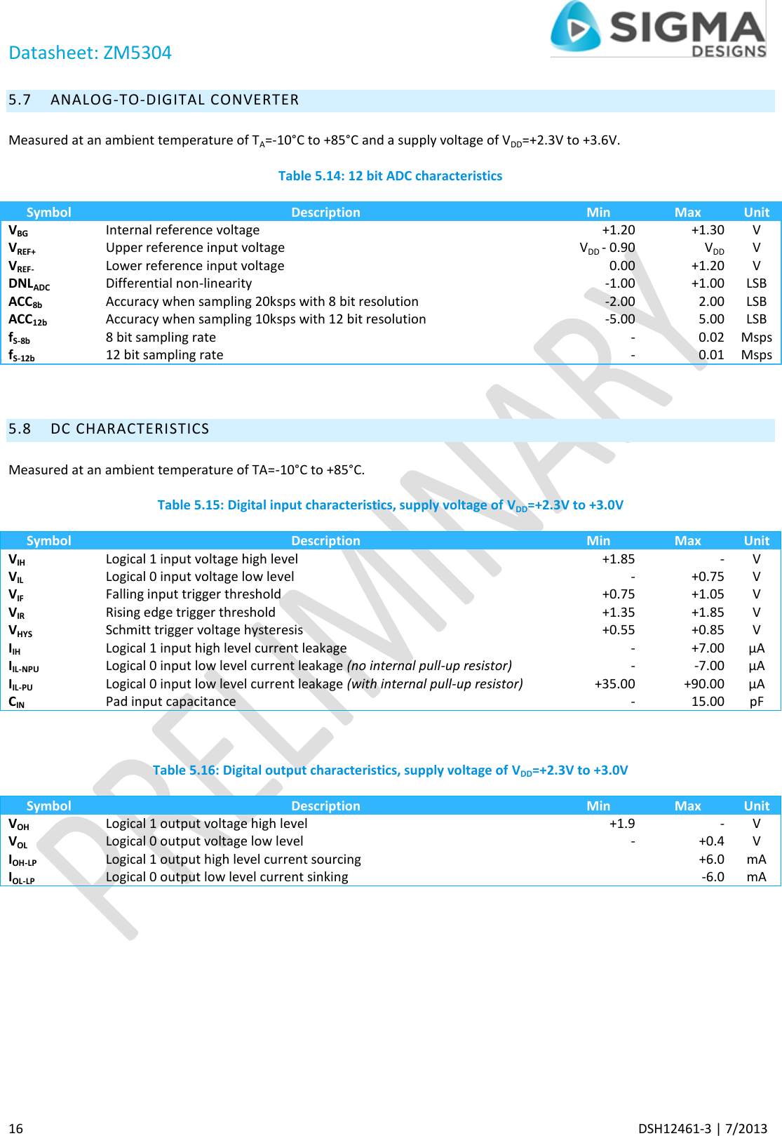
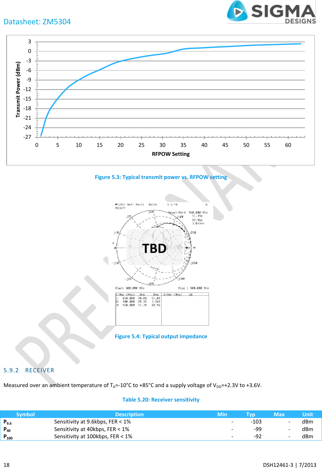
![Datasheet: ZM5304 12 DSH12461-3 | 7/2013 5 ELECTRICAL CHARACTERISTICS This section describes the electrical parameters of the ZM5304 Modem module. 5.1 TEST CONDITIONS Final Test in Production(TA=+25°C, VDD=+3.3V)Characterization in Lab(TA=-10°C to +85°C, VDD=+2.3 to +3.6V)Statistics with Min, Typ, and Max valuesSorting criterion specified with Min and Max valuesManufactured ModulesTested Modules Figure 5.1: Testing flow The following conditions apply for characterization in the lab, unless otherwise noted. 1. Ambient temperature TA = -10 to +85°C 2. Supply voltage VDD = +2.3 to +3.6V 3. All tests are carried out on the ZDB5304 Z-Wave Development Board. [4] 4. Conducted transmission power is measured at the output of the SAW filter for 868.4, 908.4, 919.8, and 921.4MHz 5. Conducted receiver sensitivity is measure at the output of the SAW filter for 868.4, 908.4, 919.8, and 921.4MHz The following conditions apply for the final test in production, unless otherwise noted. 1. Ambient temperature TA = +25°C 2. Supply voltage VDD = +3.3V 3. Radiated transmission power is measured for 868.4, 908.4, 919.8, and 921.4MHz 4. Radiated receiver sensitivity is measured for 868.4, 908.4, 919.8, and 921.4MHz 5.1.1 TYPICAL VALUES Unless otherwise specified, typical data refer to the mean of a data set measured at an ambient temperature of TA=25°C and supply voltage of VDD=+3.3V. 5.1.2 MINIMUM AND MAXIMUM VALUES Unless otherwise specified the minimum and maximum values are guaranteed in the worst conditions of ambient temperature, supply voltage and frequencies by a final test in production on 100% of the devices at an ambient temperature of TA=25°C and supply voltage of VDD=+3.3V. For data based on measurements, the minimum and maximum values represent the mean value plus or minus three times the standard deviation (µ±3σ).](https://usermanual.wiki/Sigma-Designs/ZM5304-U/User-Guide-2052478-Page-12.png)
![Datasheet: ZM5304 32 DSH12461-3 | 7/2013 11 REFERENCES [1] Sigma Designs, “Serial API Host Application Programming Guide,” INS12350, Denmark, 2012. [2] Sigma Designs, “Z-Wave 500 Series Application Programmers Guide v6.50.00,” INS12308, Denmark, 2012. [3] Sigma Designs, “500 Series Z-Wave Single Chip Programming Mode,” INS11681, Denmark, 2012. [4] Sigma Designs, “ZDB5304 Z-Wave Development Board,” DSH12468, Denmark, 2013.](https://usermanual.wiki/Sigma-Designs/ZM5304-U/User-Guide-2052478-Page-32.png)