UAB Teltonika GM14TLTK6 4 bands GSM/GPRS module User Manual TM11Q User Manual 1 0
UAB "Teltonika" 4 bands GSM/GPRS module TM11Q User Manual 1 0
UserManual.wiki
>
UAB Teltonika
>
GM14TLTK6 User Manual
user manual
Navigation menu
Upload a User Manual
Namespaces
Wiki Guide
HTML
PDF
Info
Views
User Manual
Discussion / Help
Navigation
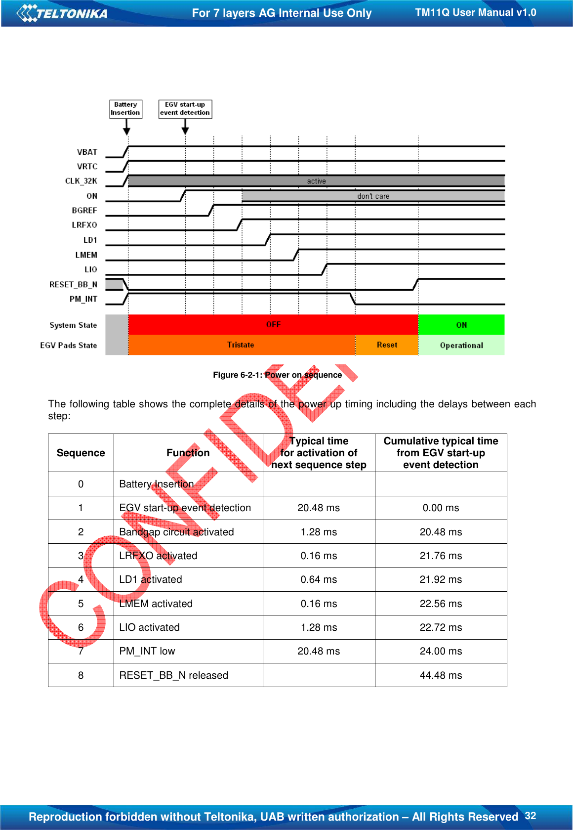
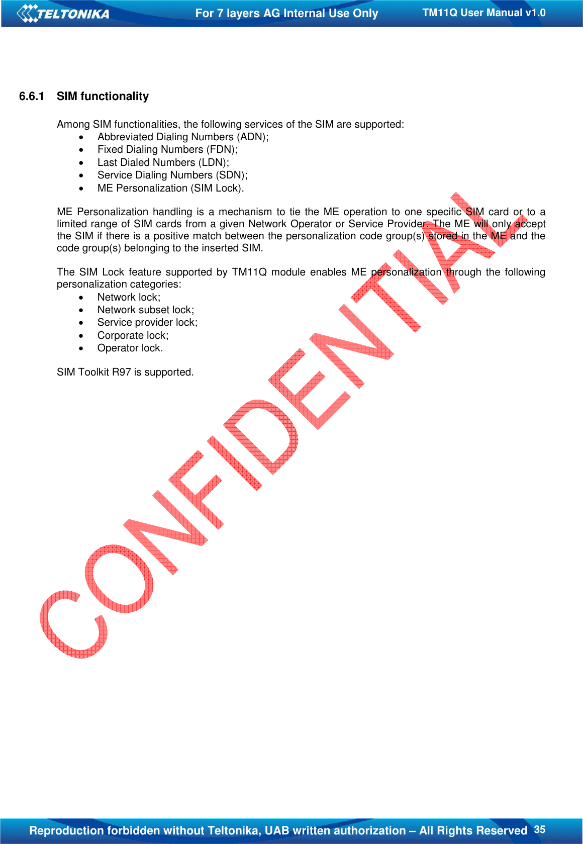
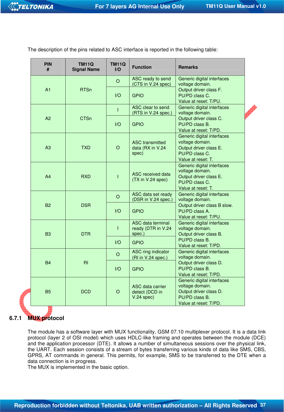
![36TM11Q User Manual v1.0 For 7 layers AG Internal Use Only Reproduction forbidden without Teltonika, UAB written authorization – All Rights Reserved 6.7 Asynchronous serial interface (ASC) The asynchronous serial interface (ASC) relies on the Asynchronous Serial Controller hardware block provided by the baseband core. ASC features are: • Complete 9-pin serial port in compliance with the ITU V.24 specifications [E.1] (i.e. a complete RS-232 low voltage interface with hardware flow control is available); • The maximum data rate is 921600 bps for software download; • Intermediate data rates can be 2400, 4800, 9600, 19200, 38400, 57600, 115200, 230400, 460800 bps with No/Even/Odd parity, 7 or 8 bit frame length; • Power saving CTS indication available at the interface (see [I.2]). Software services available at ASC: • AT interface in compliance with GSM 27.007 [E.2]: the default speed for the AT interface is 115200 bps, the maximum speed is 230400 bps (see [I.1]); • MUX protocol available in compliance with GMS 27.010 [E.3]; • Interface can be configured to access this port for customer specific usage by AT commands. The serial port is limited to 921600 bps due to the FTDI level translator (serial to USB converter) of the motherboard. A more detailed description regarding software services and serial port behavior of the module are provided by the Teltonika documents: TM11Q_AT_Commands_Manual_8MB and TM1Q_HW_Manual_1.0. This is the ITU V.24 signals naming convention [E.1]: the module is a Data Communication Equipment (DCE), which is a modem; the external host processor or the PC is the Data Terminal Equipment (DTE). Figure 6-7-1: DTE-DCE RS232 interface ITU V.24 conventional directions are in the previous figure like circuits numbers; please note that the hardware names of the module pins do not necessary reveal the ITU V.24 functionality. To download the code, only the two data lines (TXD and RXD) can be used. The other lines (CTS, RTS, DSR, RI, DCD and DTR) can be configured as GPIO.](https://usermanual.wiki/UAB-Teltonika/GM14TLTK6/User-Guide-1566172-Page-36.png)