Zhejiang Lierda Internet of Things technology NB05-01 NB-IoT Module(LTE) User Manual NB05 01 rev2x
Zhejiang Lierda Internet of Things technology Co.,Ltd NB-IoT Module(LTE) NB05 01 rev2x
UserManual.wiki
>
Zhejiang Lierda Internet of Things technology
>
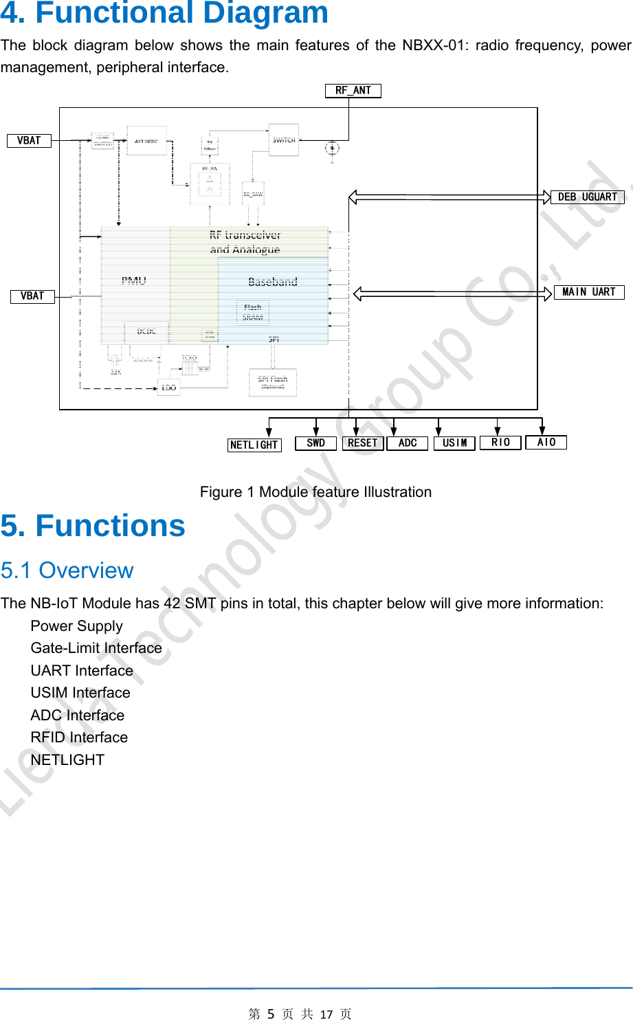
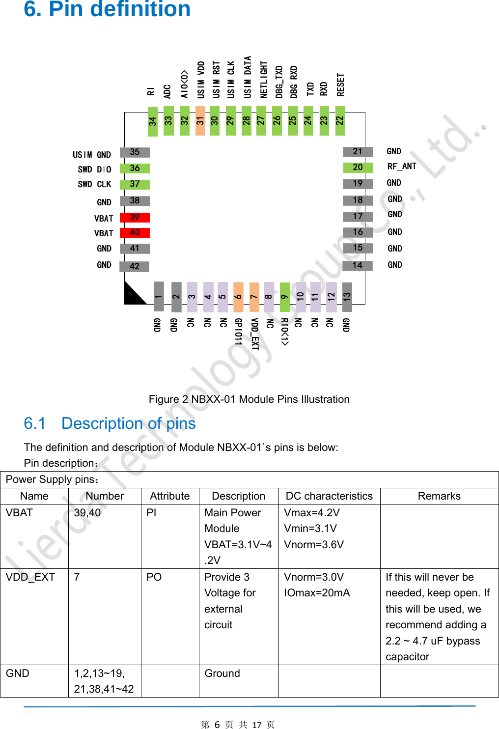
NB05 01 User Manual
Users Manual
Navigation menu
Upload a User Manual
Namespaces
Wiki Guide
HTML
PDF
Info
Views
User Manual
Discussion / Help
Navigation