u blox SARAU280 UMTS Voice and Data Module User Manual SARA G3 and SARA U2 series
u-blox AG UMTS Voice and Data Module SARA G3 and SARA U2 series
UserManual.wiki
>
u blox
>
SARAU280 User Manual
User Manual
Navigation menu
Upload a User Manual
Namespaces
Wiki Guide
HTML
PDF
Info
Views
User Manual
Discussion / Help
Navigation
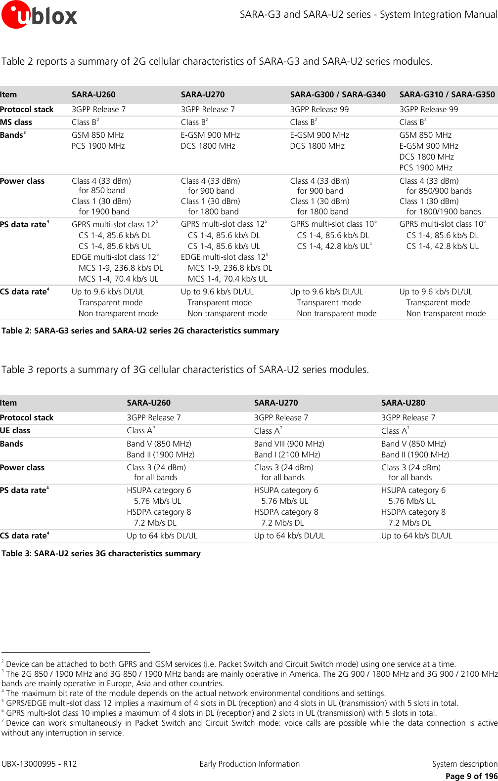
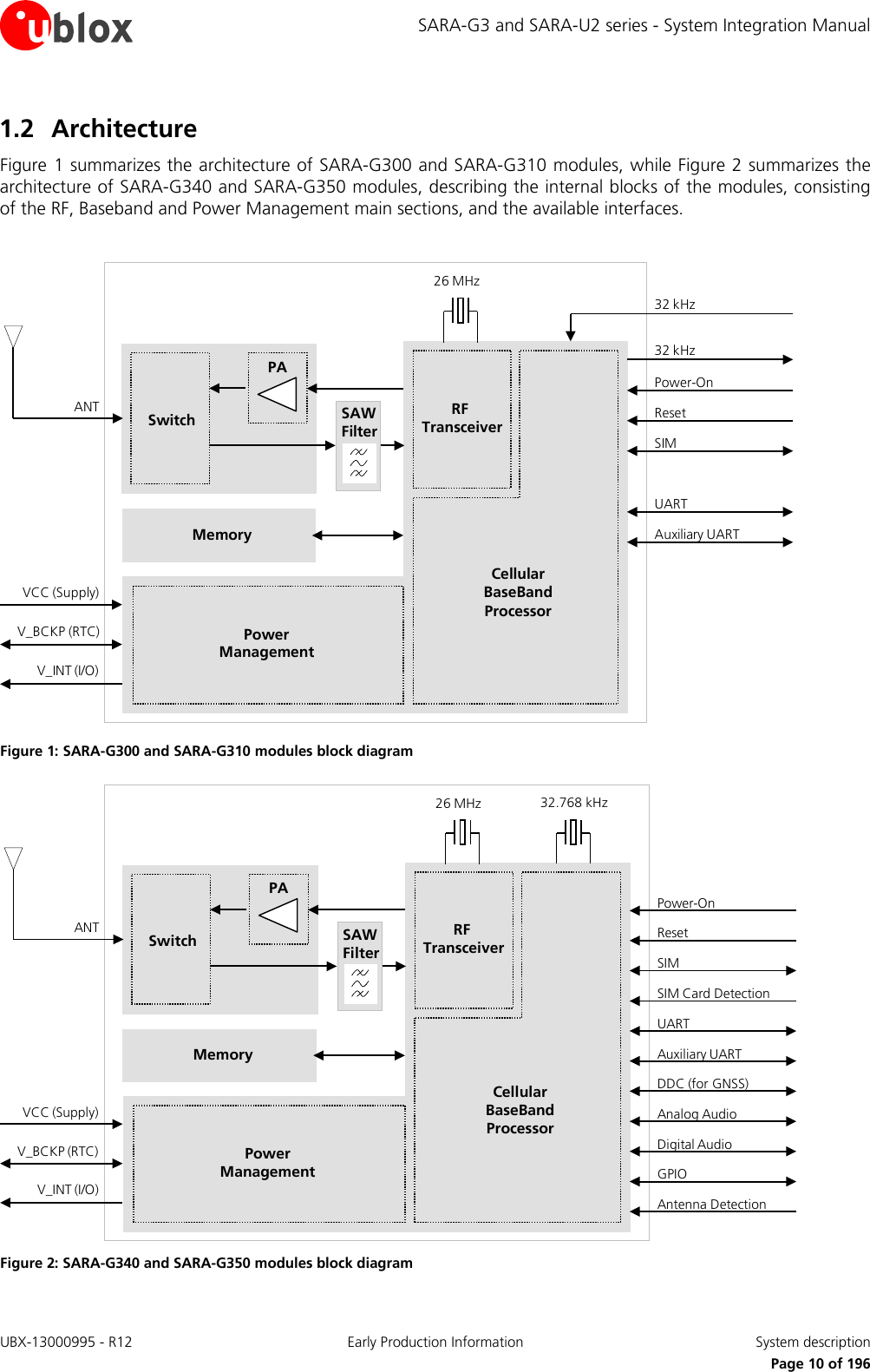
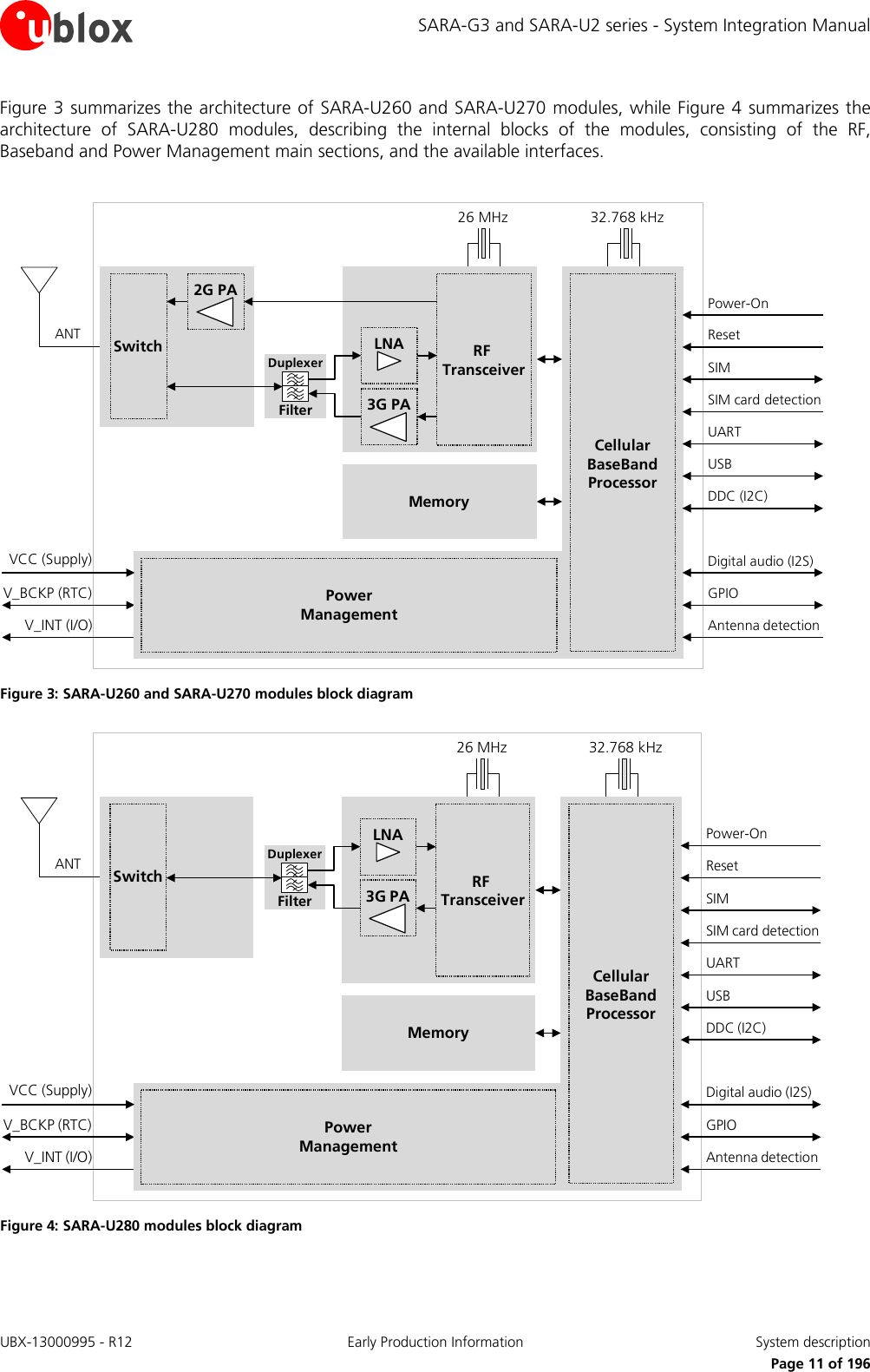
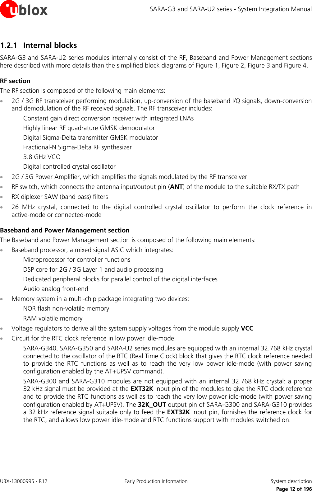
![SARA-G3 and SARA-U2 series - System Integration Manual 1 System description 1.1 Overview SARA-G3 series GSM/GPRS cellular modules and SARA-U2 series GSM/EGPRS/HSPA cellular modules are versatile solutions offering voice and/or data communication over diverse radio access technologies in the same miniature SARA LGA form factor (26 x 16 mm) that allows seamless drop-in migration between the two SARA-G3 and SARA-U2 series and easy migration to u-blox LISA-U series GSM/EGPRS/HSPA+ modules, LISA-C2 series CDMA modules, TOBY-L1 series LTE modules and to TOBY-L2 series GSM/EGPRS/DC-HSPA+/LTE modules. SARA-G350 and SARA-G340 are respectively quad-band and dual-band full feature GSM/GPRS cellular modules with a comprehensive feature set including an extensive set of internet protocols and access to u-blox GNSS positioning chips and modules, with embedded A-GPS (AssistNow Online and AssistNow Offline) functionality. SARA-G310 and SARA-G300 are respectively quad-band and dual-band GSM/GPRS cellular modules targeted for high volume cost sensitive applications, providing GSM/GPRS functionalities with a reduced set of additional features to minimize the customer’s total cost of ownership. SARA-U2 series include variants supporting band combination for North America and band combination for Europe, Asia and other countries. For each combination, a complete UMTS/GSM variant and a cost-saving UMTS-only variant are available. All SARA-U2 series modules provide a rich feature set including an extensive set of internet protocols, dual-stack IPv4 / IPv6 and access to u-blox GNSS positioning chips and modules, with embedded A-GPS (AssistNow Online and AssistNow Offline) functionality. Table 1 describes a summary of interfaces and features provided by SARA-G3 and SARA-U2 series modules. Module Data rate Bands Interfaces Audio Functions Grade 3G Up-Link [Mb/s] 3G Down-Link [Mb/s] 2G Up-Link [kb/s] 2G Down-Link [kb/s] 3G bands [MHz] 2G bands [MHz] UART USB DDC (I2C) GPIO Analog audio Digital audio Network indication Antenna supervisor Jamming detection Embedded TCP / UDP Embedded HTTP, FTP Embedded SSL / TLS GNSS via Modem AssistNow Software CellLocate® FW update via serial FOTA eCall / ERA-GLONASS Low power idle-mode Dual stack IPv4/IPv6 ATEX certification Standard Professional Automotive SARA-G300 42.8 85.6 900/1800 2 • E SARA-G310 42.8 85.6 4-band 2 • E SARA-G340 42.8 85.6 900/1800 2 1 4 1 1 • • • • • V • • • • • • SARA-G350 42.8 85.6 4-band 2 1 4 1 1 • • • • • V • • • • A • • SARA-G350 ATEX 42.8 85.6 4-band 2 1 4 1 1 • • • • • • • • • • • • SARA-U260 5.76 7.2 85.6 236.8 850/1900 850/1900 1 1 1 9 1 • • • • • • • • • • • • SARA-U270 5.76 7.2 85.6 236.8 900/2100 900/1800 1 1 1 9 1 • • • • • • • • • • • • • SARA-U270 ATEX 5.76 7.2 85.6 236.8 900/2100 900/1800 1 1 1 9 1 • • • • • • • • • • • • • • SARA-U280 5.76 7.2 850/1900 1 1 1 9 1 • • • • • • • • • • • • A = available upon request V = available from product version “01” onwards E = 32 kHz signal at EXT32K input pin is required for low power idle-mode Table 1: SARA-G3 and SARA-U2 series1 features summary 1 SARA-G350 ATEX modules provide the same feature set of the SARA-G350 modules plus the certification for use in potentially explosive atmospheres; the same applies for SARA-U270 ATEX modules and SARA-U270 modules. Unless otherwise specified, SARA-G350 refers to all SARA-G350 ATEX and SARA-G350 modules, whereas SARA-U270 refers to all SARA-U270 ATEX modules and SARA-U270 modules. UBX-13000995 - R12 Early Production Information System description Page 8 of 196](https://usermanual.wiki/u-blox/SARAU280/User-Guide-2520608-Page-8.png)
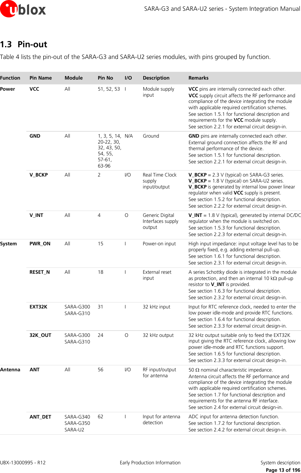
![SARA-G3 and SARA-U2 series - System Integration Manual Function Pin Name Module Pin No I/O Description Remarks Auxiliary UART RXD_AUX SARA-G3 28 O Auxiliary UART data output 1.8 V output, Circuit 104 (RXD) in ITU-T V.24, for FW upgrade via EasyFlash tool and diagnostic. Access by external test-point is recommended. See section 1.9.2 for functional description. See section 2.6.2 for external circuit design-in. TXD_AUX SARA-G3 29 I Auxiliary UART data input 1.8 V input, Circuit 103 (TXD) in ITU-T V.24, for FW upgrade via EasyFlash tool and diagnostic. Access by external test-point is recommended. Internal active pull-up to V_INT. See section 1.9.2 for functional description. See section 2.6.2 for external circuit design-in. USB VUSB_DET SARA-U2 17 I USB detect input High-Speed USB 2.0 interface input for VBUS (5 V typical) USB supply sense. USB available for AT, data, FOAT, FW upgrade via EasyFlash tool and diagnostic. See section 1.9.3 for functional description. See section 2.6.3 for external circuit design-in. USB_D- SARA-U2 28 I/O USB Data Line D- High-Speed USB 2.0 interface data line for AT, data, FOAT, FW upgrade via EasyFlash tool and diagnostic. 90 Ω nominal differential impedance. Pull-up, pull-down and series resistors as required by USB 2.0 specifications [14] are part of the USB pin driver and need not be provided externally. See section 1.9.3 for functional description. See section 2.6.3 for external circuit design-in. USB_D+ SARA-U2 29 I/O USB Data Line D+ High-Speed USB 2.0 interface data line for AT, data, FOAT, FW upgrade via EasyFlash tool and diagnostic. 90 Ω nominal differential impedance. Pull-up, pull-down and series resistors as required by USB 2.0 specifications [14] are part of the USB pin driver and need not be provided externally. See section 1.9.3 for functional description. See section 2.6.3 for external circuit design-in. DDC SCL SARA-G340 SARA-G350 SARA-U2 27 O I2C bus clock line 1.8 V open drain, for the communication with the u-blox positioning modules / chips. Communication with other external I2C-slave devices as an audio codec is additionally supported by SARA-U2 series. External pull-up required. See section 1.9.4 for functional description. See section 2.6.4 for external circuit design-in. SDA SARA-G340 SARA-G350 SARA-U2 26 I/O I2C bus data line 1.8 V open drain, for the communication with u-blox positioning modules / chips. Communication with other external I2C-slave devices as an audio codec is additionally supported by SARA-U2 series. External pull-up required. See section 1.9.4 for functional description. See section 2.6.4 for external circuit design-in. UBX-13000995 - R12 Early Production Information System description Page 15 of 196](https://usermanual.wiki/u-blox/SARAU280/User-Guide-2520608-Page-15.png)
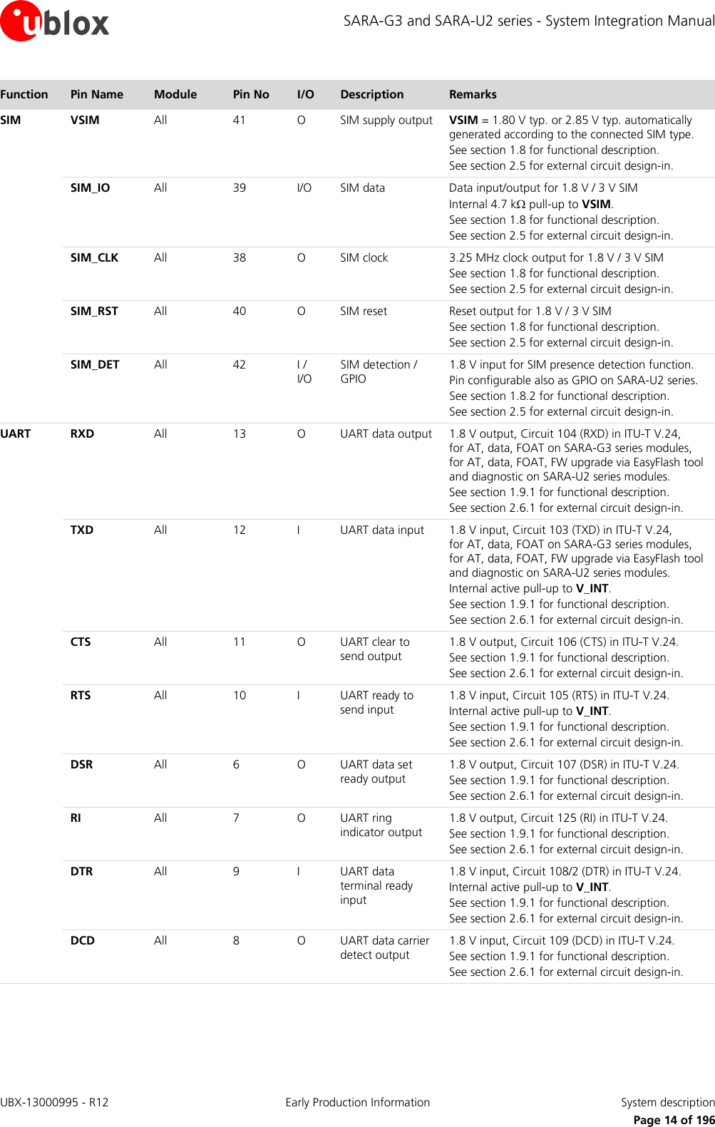
![SARA-G3 and SARA-U2 series - System Integration Manual 1.4 Operating modes SARA-G3 modules have several operating modes. The operating modes defined in Table 5 and described in detail in Table 6 provide general guidelines for operation. General Status Operating Mode Definition Power-down Not-Powered Mode VCC supply not present or below operating range: module is switched off. Power-Off Mode VCC supply within operating range and module is switched off. Normal Operation Idle-Mode Module processor core runs with 32 kHz reference, that is generated by: • The internal 32 kHz oscillator (SARA-G340, SARA-G350 and SARA-U2 series) • The 32 kHz signal provided at the EXT32K pin (SARA-G300 and SARA-G310) Active-Mode Module processor core runs with 26 MHz reference generated by the internal oscillator. Connected-Mode Voice or data call enabled and processor core runs with 26 MHz reference. Table 5: Module operating modes definition Operating Mode Description Transition between operating modes Not-Powered Module is switched off. Application interfaces are not accessible. Internal RTC operates on SARA-G340/G350, SARA-U2 if a valid voltage is applied to V_BCKP. Additionally, a proper external 32 kHz signal must be fed to EXT32K on SARA-G300/G310 modules to let internal RTC timer running. When VCC supply is removed, the module enters not-powered mode. When in not-powered mode, the modules cannot be switched on by PWR_ON, RESET_N or RTC alarm. When in not-powered mode, the modules can be switched on applying VCC supply (see 2.3.1) so that the module switches from not-powered to active-mode. Power-Off Module is switched off: normal shutdown by an appropriate power-off event (see 1.6.2). Application interfaces are not accessible. Internal RTC operates on SARA-G340/G350, SARA-U2 as V_BCKP is internally generated. A proper external 32 kHz signal must be fed to the EXT32K pin on SARA-G300/G310 to let RTC timer running that otherwise is not in operation. When the module is switched off by an appropriate power-off event (see 1.6.2), the module enters power-off mode from active-mode. When in power-off mode, the modules can be switched on by PWR_ON, RESET_N or RTC alarm (see 2.3.1): the module switches from power-off to active-mode. When VCC supply is removed, the module switches from power-off mode to not-powered mode. Idle The module is not ready to communicate with an external device by means of the application interfaces as configured to reduce consumption. The module automatically enters idle-mode whenever possible if power saving is enabled by the AT+UPSV command (see u-blox AT Commands Manual [3]), reducing power consumption (see section 1.5.1.4). The CTS output line indicates when the UART interface is disabled/enabled due to the module idle/active-mode according to power saving and HW flow control settings (see 1.9.1.3, 1.9.1.4). Power saving configuration is not enabled by default: it can be enabled by AT+UPSV (see the u-blox AT Commands Manual [3]). A proper 32 kHz signal must be fed to the EXT32K pin of SARA-G300/G310 modules to let idle-mode that otherwise cannot be reached (this is not needed for the other SARA-G3 and SARA-U2 series modules). The module automatically switches from active-mode to idle-mode whenever possible if power saving is enabled (see sections 1.5.1.4, 1.9.1.4 and to the u-blox AT Commands Manual [3], AT+UPSV). The module wakes up from idle to active mode in the following events: • Automatic periodic monitoring of the paging channel for the paging block reception according to network conditions (see 1.5.1.4, 1.9.1.4) • Automatic periodic enable of the UART interface to receive and send data, if AT+UPSV=1 power saving is set (see 1.9.1.4) • RTC alarm occurs (see u-blox AT Commands Manual [3], +CALA) • Data received on UART interface, according to HW flow control (AT&K) and power saving (AT+UPSV) settings (see 1.9.1.4) • RTS input line set to the ON state by the DTE, if HW flow control is disabled by AT&K3 and AT+UPSV=2 is set (see 1.9.1.4) • DTR input line set to the ON state by the DTE, if AT+UPSV=3 power saving is set (see 1.9.1.4) • USB detection, applying 5 V (typ.) to VUSB_DET input (see 1.9.3) • The connected USB host forces a remote wakeup of the module as USB device (see 1.9.3) • GNSS data ready: when the GPIO3 pin is informed by the connected u-blox GNSS receiver that it is ready to send data over the DDC (I2C) communication interface (see 1.11, 1.9.4) UBX-13000995 - R12 Early Production Information System description Page 18 of 196](https://usermanual.wiki/u-blox/SARAU280/User-Guide-2520608-Page-18.png)
![SARA-G3 and SARA-U2 series - System Integration Manual Operating Mode Description Transition between operating modes Active The module is ready to communicate with an external device by means of the application interfaces unless power saving configuration is enabled by the AT+UPSV command (see sections 1.5.1.4, 1.9.1.4 and to the u-blox AT Commands Manual [3]). When the module is switched on by an appropriate power-on event (see 2.3.1), the module enters active-mode from not-powered or power-off mode. If power saving configuration is enabled by the AT+UPSV command, the module automatically switches from active to idle-mode whenever possible and the module wakes up from idle to active-mode in the events listed above (see idle to active transition description). When a voice call or a data call is initiated, the module switches from active-mode to connected-mode. Connected A voice call or a data call is in progress. The module is ready to communicate with an external device by means of the application interfaces unless power saving configuration is enabled by the AT+UPSV command (see sections 1.5.1.4, 1.9.1.4 and the u-blox AT Commands Manual [3]). When a voice call or a data call is initiated, the module enters connected-mode from active-mode. When a voice call or a data call is terminated, the module returns to the active-mode. Table 6: Module operating modes description Figure 5 describes the transition between the different operating modes. Switch ON:•Apply VCCIf power saving is enabled and there is no activity for a defined time intervalAny wake up event described in the module operating modes summary table aboveIncoming/outgoing call or other dedicated device network communicationNo RF Tx/Rx in progress, Call terminated, Communication droppedRemove VCCSwitch ON:•PWR_ON•RTC alarm•RESET_N (SARA-U2)Not poweredPower offActiveConnected IdleSwitch OFF:•AT+CPWROFF•PWR_ON (SARA-U2) Figure 5: Operating modes transition UBX-13000995 - R12 Early Production Information System description Page 19 of 196](https://usermanual.wiki/u-blox/SARAU280/User-Guide-2520608-Page-19.png)
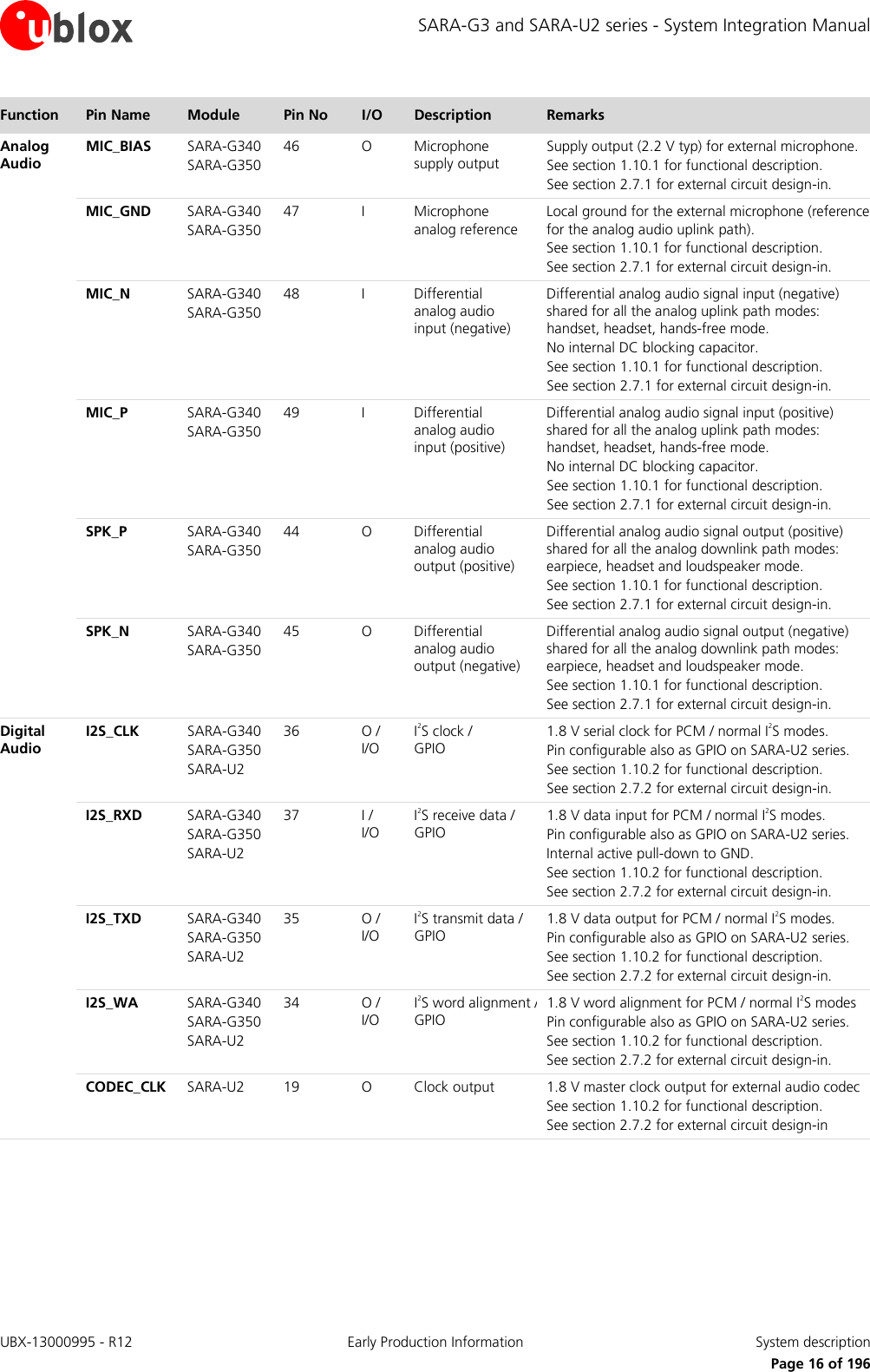
![SARA-G3 and SARA-U2 series - System Integration Manual 1.5 Supply interfaces 1.5.1 Module supply input (VCC) The modules must be supplied via the three VCC pins that represent the module power supply input. The VCC pins are internally connected to the RF power amplifier and to the integrated Power Management Unit: all supply voltages needed by the module are generated from the VCC supply by integrated voltage regulators, including V_BCKP Real Time Clock supply, V_INT digital interfaces supply and VSIM SIM card supply. During operation, the current drawn by the SARA-G3 and SARA-U2 series modules through the VCC pins can vary by several orders of magnitude. This ranges from the high peak of current consumption during GSM transmitting bursts at maximum power level in connected-mode (as described in section 1.5.1.2), to the low current consumption during low power idle-mode with power saving enabled (as described in section 1.5.1.4). 1.5.1.1 VCC supply requirements Table 7 summarizes the requirements for the VCC module supply. See section 2.2.1 for all the suggestions to properly design a VCC supply circuit compliant to the requirements listed in Table 7. VCC supply circuit affects the RF compliance of the device integrating SARA-G3 and SARA-U2 series modules with applicable required certification schemes as well as antenna circuit design. Compliance is guaranteed if the VCC requirements summarized in the Table 7 are fulfilled. For the additional specific requirements for SARA-G350 ATEX and SARA-U270 ATEX modules integration in potentially explosive atmospheres applications, see section 2.14. Item Requirement Remark VCC nominal voltage Within VCC normal operating range: 3.35 V min. / 4.50 V max for SARA-G3 series 3.30 V min. / 4.40 V max for SARA-U2 series The module cannot be switched on if VCC voltage value is below the normal operating range minimum limit. Ensure that the input voltage at VCC pins is above the minimum limit of the normal operating range for at least more than 3 s after the module switch-on. VCC voltage during normal operation Within VCC extended operating range: 3.00 V min. / 4.50 V max for SARA-G3 series 3.10 V min. / 4.50 V max for SARA-U2 series The module may switch off when VCC voltage drops below the extended operating range minimum limit. Operation above extended operating range limit is not recommended and may affect device reliability. VCC average current Support with adequate margin the highest averaged VCC current consumption value in connected-mode conditions specified in SARA-G3 series Data Sheet [1] and in SARA-U2 series Data Sheet [2]. The highest averaged VCC current consumption can be greater than the specified value according to the actual antenna mismatching, temperature and VCC voltage. See 1.5.1.2, 1.5.1.3 for connected-mode current profiles. VCC peak current Support with margin the highest peak VCC current consumption value specified in SARA-G3 series Data Sheet [1] and in SARA-U2 series Data Sheet [2]. The specified highest peak of VCC current consumption occurs during GSM single transmit slot in 850/900 MHz connected-mode, in case of mismatched antenna. See 1.5.1.2 for 2G connected-mode current profiles. VCC voltage drop during 2G Tx slots Lower than 400 mV VCC voltage drop directly affects the RF compliance with applicable certification schemes. Figure 7 describes VCC voltage drop during Tx slots. VCC voltage ripple during 2G/3G Tx Lower than 50 mVpp if fripple ≤ 200 kHz Lower than 10 mVpp if 200 kHz < fripple ≤ 400 kHz Lower than 2 mVpp if fripple > 400 kHz VCC voltage ripple directly affects the RF compliance with applicable certification schemes. Figure 7 describes VCC voltage ripple during Tx slots. VCC under/over-shoot at start/end of Tx slots Absent or at least minimized VCC under/over-shoot directly affects the RF compliance with applicable certification schemes. Figure 7 describes VCC voltage under/over-shoot. Table 7: Summary of VCC supply requirements UBX-13000995 - R12 Early Production Information System description Page 20 of 196](https://usermanual.wiki/u-blox/SARAU280/User-Guide-2520608-Page-20.png)
![SARA-G3 and SARA-U2 series - System Integration Manual 1.5.1.2 VCC current consumption in 2G connected-mode When a GSM call is established, the VCC consumption is determined by the current consumption profile typical of the GSM transmitting and receiving bursts. The current consumption peak during a transmission slot is strictly dependent on the transmitted power, which is regulated by the network. The transmitted power in the transmit slot is also the more relevant factor for determining the average current consumption. If the module is transmitting in 2G single-slot mode (as in GSM talk mode) in the 850 or 900 MHz bands, at the maximum RF power control level (approximately 2 W or 33 dBm in the Tx slot/burst), the current consumption can reach an high peak / pulse (see SARA-G3 series Data Sheet [1] and SARA-U2 series Data Sheet [2]) for 576.9 µs (width of the transmit slot/burst) with a periodicity of 4.615 ms (width of 1 frame = 8 slots/burst), so with a 1/8 duty cycle according to GSM TDMA (Time Division Multiple Access). If the module is transmitting in 2G single-slot mode in the 1800 or 1900 MHz bands, the current consumption figures are quite less high than the one in the low bands, due to 3GPP transmitter output power specifications. During a GSM call, current consumption is not so significantly high in receiving or in monitor bursts and it is low in the bursts unused to transmit / receive. Figure 6 shows an example of the module current consumption profile versus time in GSM talk mode. Time [ms]RX slotunused slotunused slotTX slotunused slotunused slotMON slotunused slotRX slotunused slotunused slotTX slotunused slotunused slotMON slotunused slotGSM frame 4.615 ms (1 frame = 8 slots)Current [A]200 mA60-120 mA1900 mAPeak current depends on TX power and actual antenna loadGSM frame 4.615 ms (1 frame = 8 slots)1.51.00.50.02.060-120 mA10-40 mA Figure 6: VCC current consumption profile versus time during a GSM call (1 TX slot, 1 RX slot) Figure 7 illustrates VCC voltage profile versus time during a GSM call, according to the related VCC current consumption profile described in Figure 6. TimeundershootovershootrippledropVoltage3.8 V (typ)RX slotunused slotunused slotTX slotunused slotunused slotMON slotunused slotRX slotunused slotunused slotTX slotunused slotunused slotMON slotunused slotGSM frame 4.615 ms (1 frame = 8 slots)GSM frame 4.615 ms (1 frame = 8 slots) Figure 7: Description of the VCC voltage profile versus time during a GSM call (1 TX slot, 1 RX slot) UBX-13000995 - R12 Early Production Information System description Page 21 of 196](https://usermanual.wiki/u-blox/SARAU280/User-Guide-2520608-Page-21.png)
![SARA-G3 and SARA-U2 series - System Integration Manual When a GPRS connection is established, more than one slot can be used to transmit and/or more than one slot can be used to receive. The transmitted power depends on network conditions, which set the peak current consumption, but following the GPRS specifications the maximum transmitted RF power is reduced if more than one slot is used to transmit, so the maximum peak of current is not as high as can be in case of a GSM call. If the module transmits in GPRS multi-slot class 10 or 12, in 850 or 900 MHz bands, at maximum RF power level, the consumption can reach a quite high peak but lower than the one achievable in 2G single-slot mode. This happens for 1.154 ms (width of the 2 Tx slots/bursts) in case of multi-slot class 10 or for 2.308 ms (width of the 4 Tx slots/bursts) in case of multi-slot class 12, with a periodicity of 4.615 ms (width of 1 frame = 8 slots/bursts), so with a 1/4 or 1/2 duty cycle, according to GSM TDMA. If the module is in GPRS connected-mode in 1800 or 1900 MHz bands, consumption figures are lower than in the 850 or 900 MHz band, due to 3GPP Tx power specifications. Figure 8 reports the current consumption profiles in GPRS connected-mode, in the 850 or 900 MHz bands, with 2 slots used to transmit and 1 slot used to receive, as for the GPRS multi-slot class 10. Time [ms]RX slotunused slotunused slotTX slotTX slotunused slotMON slotunused slotRX slotunused slotunused slotTX slotTX slotunused slotMON slotunused slotGSM frame 4.615 ms (1 frame = 8 slots)Current [A]60-120mAGSM frame 4.615 ms (1 frame = 8 slots)1.51.00.50.060-120mA 10-40mA200mAPeak current depends on TX power and actual antenna load1600 mA Figure 8: VCC current consumption profile versus time during a GPRS multi-slot class 10 connection (2 TX slots, 1 RX slot) Figure 9 reports the current consumption profiles in GPRS connected-mode, in the 850 or 900 MHz bands, with 4 slots used to transmit and 1 slot used to receive, as for the GPRS multi-slot class 12. Time [ms]RX slotunused slotTX slotTX slotTX slotTX slotMON slotunused slotRX slotunused slotTX slotTX slotTX slotTX slotMON slotunused slotGSM frame 4.615 ms (1 frame = 8 slots)Current [A]60-120mAGSM frame 4.615 ms (1 frame = 8 slots)1.51.00.50.060-120mA10-40mA200mAPeak current depends on TX power and actual antenna load1600 mA Figure 9: VCC current consumption profile versus time during a GPRS multi-slot class 12 connection (4 TX slots, 1 RX slot) For detailed current consumption values during 2G single-slot or multi-slot connection see SARA-G3 series Data Sheet [1] and SARA-U2 series Data Sheet [2]. UBX-13000995 - R12 Early Production Information System description Page 22 of 196](https://usermanual.wiki/u-blox/SARAU280/User-Guide-2520608-Page-22.png)
![SARA-G3 and SARA-U2 series - System Integration Manual 1.5.1.3 VCC current consumption in 3G connected mode During a 3G connection, the SARA-U2 modules can transmit and receive continuously due to the Frequency Division Duplex (FDD) mode of operation with the Wideband Code Division Multiple Access (WCDMA). The current consumption depends again on output RF power, which is always regulated by network commands. These power control commands are logically divided into a slot of 666 µs, thus the rate of power change can reach a maximum rate of 1.5 kHz. There are no high current peaks as in the 2G connection, since transmission and reception are continuously enabled due to FDD WCDMA implemented in the 3G that differs from the TDMA implemented in the 2G case. In the worst scenario, corresponding to a continuous transmission and reception at maximum RF output power (approximately 250 mW or 24 dBm), the average current drawn by the module at the VCC pins is high (see the SARA-U2 series Data Sheet [2]). Even at lowest RF output power level (approximately 0.01 µW or -50 dBm), the average current is still not so low as in the equivalent 2G case, also due to module continuous baseband processing and transceiver activity. Figure 10 shows an example of current consumption profile of SARA-U2 series modules in 3G WCDMA/HSPA continuous transmission and reception mode. For detailed current consumption values during a 3G connection see the SARA-U2 series Data Sheet [2]. Time [ms]3G frame 10 ms (1 frame = 15 slots)Current [mA]Current consumption depends on TX power and actual antenna load170 mA1 slot 666 µs850 mA0300200100500400600700800 Figure 10: VCC current consumption profile versus time during a 3G connection (TX and RX continuously enabled) UBX-13000995 - R12 Early Production Information System description Page 23 of 196](https://usermanual.wiki/u-blox/SARAU280/User-Guide-2520608-Page-23.png)
![SARA-G3 and SARA-U2 series - System Integration Manual 1.5.1.4 VCC current consumption in cyclic idle/active-mode (power saving enabled) The power saving configuration is by default disabled, but it can be enabled using the appropriate AT command (see u-blox AT Commands Manual [3], AT+UPSV command). When power saving is enabled, the module automatically enters low power idle-mode whenever possible, reducing current consumption. During idle-mode, the module processor runs with 32 kHz reference clock: • the internal oscillator automatically generates the 32 kHz clock on SARA-G340, SARA-G350, SARA-U2 series • a valid 32 kHz signal must be properly provided to the EXT32K input pin of the SARA-G300 and SARA-G310 modules to let low power idle-mode, that otherwise cannot be reached by these modules. When the power saving configuration is enabled and the module is registered or attached to a network, the module automatically enters the low power idle-mode whenever possible, but it must periodically monitor the paging channel of the current base station (paging block reception), in accordance to the 2G or 3G system requirements, even if connected-mode is not enabled by the application. When the module monitors the paging channel, it wakes up to the active-mode, to enable the reception of paging block. In between, the module switches to low power idle-mode. This is known as discontinuous reception (DRX). The module processor core is activated during the paging block reception, and automatically switches its reference clock frequency from 32 kHz to the 26 MHz used in active-mode. The time period between two paging block receptions is defined by the network. This is the paging period parameter, fixed by the base station through broadcast channel sent to all users on the same serving cell. • In case of 2G radio access technology, the paging period varies from 470.8 ms (DRX = 2, length of 2 x 51 2G frames = 2 x 51 x 4.615 ms) up to 2118.4 ms (DRX = 9, length of 9 x 51 2G frames = 9 x 51 x 4.615 ms) • In case of 3G radio access technology, the paging period can vary from 640 ms (DRX = 6, i.e. length of 26 3G frames = 64 x 10 ms) up to 5120 ms (DRX = 9, length of 29 3G frames = 512 x 10 ms). Figure 11 roughly describes the current consumption profile of SARA-G300 and SARA-G310 modules (when their EXT32K input pin is fed by an external 32 kHz signal with characteristics compliant to the one specified in SARA-G3 series Data Sheet [1]), or the SARA-G340 and SARA-G350 modules, or the SARA-U2 modules, when power saving is enabled. The module is registered with the network, automatically enters the very low power idle-mode, and periodically wakes up to active-mode to monitor the paging channel for paging block reception. 20-30 msIDLE MODE ACTIVE MODE IDLE MODE300-600 µAActive Mode EnabledIdle Mode Enabled300-600 µA60-120 mA2G case: 0.44-2.09 s 3G case: 0.61-5.09 sIDLE MODE20-30 msACTIVE MODETime [s]Current [mA]100500Time [ms]Current [mA]1005004-5 mA60-120 mARX Enabled20-40 mADSP Enabled Figure 11: VCC current consumption profile versus time of the SARA-G300 and SARA-G310 modules (with the EXT32K input fed by a proper external 32 kHz signal), or the SARA-G340 and SARA-G350 modules, or the SARA-U2 modules, when registered with the network, with power saving enabled: the very low power idle-mode is reached and periodical wake up to active-mode are performed to monitor the paging channel UBX-13000995 - R12 Early Production Information System description Page 24 of 196](https://usermanual.wiki/u-blox/SARAU280/User-Guide-2520608-Page-24.png)
![SARA-G3 and SARA-U2 series - System Integration Manual Figure 12 roughly describes the current consumption profile of SARA-G300 and SARA-G310 modules when the EXT32K input pin is fed by the 32K_OUT output pin provided by these modules, when power saving is enabled. The module is registered with the network, automatically enters the low power idle-mode and periodically wakes up to active-mode to monitor the paging channel for paging block reception. 20-30 msIDLE MODE ACTIVE MODE IDLE MODE3-4 mAActive Mode EnabledIdle Mode Enabled3-4 mA60-120 mA0.44-2.09 sIDLE MODE20-30 msACTIVE MODETime [s]Current [mA]100500Time [ms]Current [mA]1005004-5 mA60-120 mARX Enabled20-40 mADSP Enabled Figure 12: VCC current consumption profile versus time of the SARA-G300 and SARA-G310 modules (with the EXT32K input pin fed by the 32K_OUT output pin provided by these modules), when registered with the network, with power saving enabled: the low power idle-mode is reached and periodical wake up to active-mode are performed to monitor the paging channel For detailed current consumption values with the module registered with 2G or 3G network with power saving enabled (cyclic idle/active-mode) see SARA-G3 series Data Sheet [1] and SARA-U2 series Data Sheet [2]. UBX-13000995 - R12 Early Production Information System description Page 25 of 196](https://usermanual.wiki/u-blox/SARAU280/User-Guide-2520608-Page-25.png)
![SARA-G3 and SARA-U2 series - System Integration Manual 1.5.1.5 VCC current consumption in fixed active-mode (power saving disabled) Power saving configuration is by default disabled, or it can be disabled using the appropriate AT command (see u-blox AT Commands Manual [3], AT+UPSV command). When power saving is disabled, the module does not automatically enter idle-mode whenever possible: the module remains in active-mode. The module processor core is activated during active-mode, and the 26 MHz reference clock frequency is used. Figure 13 roughly describes the current consumption profile of the SARA-G300 and SARA-G310 modules (when the EXT32K input pin is fed by external 32 kHz signal with characteristics compliant to the one specified in SARA-G3 series Data Sheet [1], or by the 32K_OUT output pin provided by these modules), or the SARA-G340 and SARA-G350 modules (except ‘00’ versions), when power saving is disabled: the module is registered with the network, active-mode is maintained, and the receiver and the DSP are periodically activated to monitor the paging channel for paging block reception. ACTIVE MODE60-120 mA0.47-2.12 sPaging periodTime [s]Current [mA]100500Time [ms]Current [mA]1005003-5 mA60-120 mARX Enabled20-40 mADSP Enabled3-5 mA3-5 mA Figure 13: VCC current consumption profile versus time of the SARA-G300 and SARA-G310 modules (with the EXT32K input pin fed by proper external 32 kHz signal or by 32K_OUT output pin), or SARA-G340 and SARA-G350 modules (except ‘00’ versions), when registered with the network, with power saving disabled: the active-mode is always held, and the receiver and the DSP are periodically activated to monitor the paging channel UBX-13000995 - R12 Early Production Information System description Page 26 of 196](https://usermanual.wiki/u-blox/SARAU280/User-Guide-2520608-Page-26.png)
![SARA-G3 and SARA-U2 series - System Integration Manual Figure 14 roughly describes the current consumption profile of the SARA-G300 and SARA-G310 modules (when their EXT32K input is not fed by a signal, i.e. left unconnected), or the SARA-G340 and SARA-G350 modules (‘00’ versions only), or the SARA-U2 modules, when power saving is disabled: the module is registered with the network, active-mode is maintained, and the receiver and the DSP are periodically activated to monitor the paging channel for paging block reception. ACTIVE MODE10-18 mA60-120 mA2G case: 0.47-2.12 s 3G case: 0.64-5.12 sPaging periodTime [s]Current [mA]100500Time [ms]Current [mA]10050010-18 mA60-120 mARX Enabled20-40 mADSP Enabled10-18 mA Figure 14: VCC current consumption profile versus time of the SARA-G300 and SARA-G310 modules (when their EXT32K input is not fed by a signal), or the SARA-G340 and SARA-G350 modules (‘00’ versions only), or the SARA-U2 modules, when registered with the network, with power saving disabled: the active-mode is always held, and the receiver and the DSP are periodically activated to monitor the paging channel For detailed current consumption values with the module registered with 2G or 3G network with power saving disabled (fixed active-mode) see the SARA-G3 series Data Sheet [1] and SARA-U2 series Data Sheet [2]. UBX-13000995 - R12 Early Production Information System description Page 27 of 196](https://usermanual.wiki/u-blox/SARAU280/User-Guide-2520608-Page-27.png)
![SARA-G3 and SARA-U2 series - System Integration Manual 1.5.2 RTC supply input/output (V_BCKP) The V_BCKP pin of SARA-G3 and SARA-U2 series modules connects the supply for the Real Time Clock (RTC) and Power-On internal logic. This supply domain is internally generated by a linear LDO regulator integrated in the Power Management Unit, as described in Figure 15. The output of this linear regulator is always enabled when the main voltage supply provided to the module through the VCC pins is within the valid operating range, with the module switched off or switched on. Baseband Processor51VCC52VCC53VCC2V_BCKPLinear LDO RTCPower ManagementSARA-G340 / SARA-G350SARA-U2 series32 kHzBaseband Processor51VCC52VCC53VCC2V_BCKPLinear LDO RTCPower ManagementSARA-G300 / SARA-G31032 kHz31EXT32K Figure 15: RTC supply input/output (V_BCKP) and 32 kHz RTC timing reference clock simplified block diagram The RTC provides the module time reference (date and time) that is used to set the wake-up interval during the idle-mode periods between network paging, and is able to make available the programmable alarm functions. The RTC functions are available also in power-down mode when the V_BCKP voltage is within its valid range (specified in the “Input characteristics of Supply/Power pins” table in the SARA-G3 series Data Sheet [1] and SARA-U2 series Data Sheet [2]) and, for SARA-G300 / SARA-G310 modules only, when their EXT32K input pin is fed by an external 32.768 kHz signal with proper characteristics (specified in the “EXT32K pin characteristics” table in SARA-G3 series Data Sheet [1]). See the u-blox AT Commands Manual [3] for more details. The RTC can be supplied from an external back-up battery through the V_BCKP, when the main voltage supply is not provided to the module through VCC. This lets the time reference (date and time) run until the V_BCKP voltage is within its valid range, even when the main supply is not provided to the module. The RTC oscillator does not necessarily stop operation (i.e. the RTC counting does not necessarily stop) when V_BCKP voltage value drops below the specified operating range minimum limit (1.00 V): the RTC value read after a system restart could be not reliable, as explained in Table 8. V_BCKP voltage value RTC value reliability Notes 1.00 V < V_BCKP < 2.40 V RTC oscillator does not stop operation RTC value read after a restart of the system is reliable V_BCKP within operating range 0.05 V < V_BCKP < 1.00 V RTC oscillator does not necessarily stop operation RTC value read after a restart of the system is not reliable V_BCKP below operating range 0.00 V < V_BCKP < 0.05 V RTC oscillator stops operation RTC value read after a restart of the system is reliable V_BCKP below operating range Table 8: RTC value reliability as function of V_BCKP voltage value Consider that the module cannot switch on if a valid voltage is not present on VCC even when the RTC is supplied through V_BCKP (meaning that VCC is mandatory to switch on the module). UBX-13000995 - R12 Early Production Information System description Page 28 of 196](https://usermanual.wiki/u-blox/SARAU280/User-Guide-2520608-Page-28.png)
![SARA-G3 and SARA-U2 series - System Integration Manual The RTC has very low power consumption, but is highly temperature dependent. For example at 25 °C, with the V_BCKP voltage equal to the typical output value, the current consumption is approximately 2 µA (see the “Input characteristics of Supply/Power pins” table in the SARA-G3 series Data Sheet [1] and SARA-U2 series Data Sheet [2] for the detailed specification), whereas at 70 °C and an equal voltage the current consumption increases to 5-10 µA. If V_BCKP is left unconnected and the module main voltage supply is removed from VCC, the RTC is supplied from the bypass capacitor mounted inside the module. However, this capacitor is not able to provide a long buffering time: within few milliseconds the voltage on V_BCKP will go below the valid range (1 V min). This has no impact on cellular connectivity, as all the module functionalities do not rely on date and time setting. 1.5.3 Generic digital interfaces supply output (V_INT) The same 1.8 V voltage domain used internally to supply the generic digital interfaces of SARA-G3 and SARA-U2 series modules is also available on the V_INT supply output pin, as described in Figure 16. Baseband Processor51VCC52VCC53VCC4V_INTSwitchingStep-DownDigital I/O InterfacesPower ManagementSARA-G3 / SARA-U2 series Figure 16: SARA-G3 and SARA-U2 series interfaces supply output (V_INT) simplified block diagram The internal regulator that generates the V_INT supply is a switching step-down converter that is directly supplied from VCC. The voltage regulator output is set to 1.8 V (typical) when the module is switched on and it is disabled when the module is switched off. The switching regulator operates in Pulse Width Modulation (PWM) for greater efficiency at high output loads when the module is in active-mode or in connected-mode. When the module is in low power idle-mode between paging periods and with power saving configuration enabled by the appropriate AT command, it automatically switches to Pulse Frequency Modulation (PFM) for greater efficiency at low output loads. See the u-blox AT Commands Manual [3], +UPSV command. UBX-13000995 - R12 Early Production Information System description Page 29 of 196](https://usermanual.wiki/u-blox/SARAU280/User-Guide-2520608-Page-29.png)
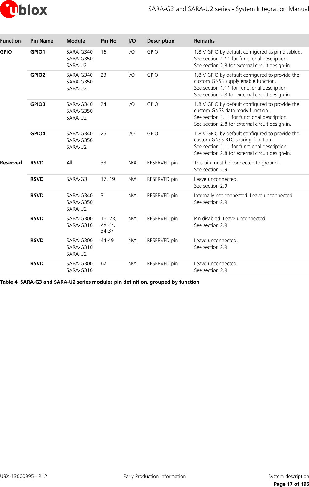
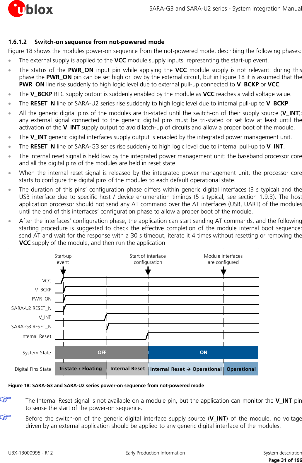
![SARA-G3 and SARA-U2 series - System Integration Manual 1.6 System function interfaces 1.6.1 Module power-on 1.6.1.1 Switch-on events Table 9 summarizes the possible switch-on events for the SARA-G3 and SARA-U2 series modules. SARA-G3 SARA-U2 From Not-Powered Mode Applying valid VCC supply voltage (i.e. VCC rise edge), ramping from 2.5 V to 3.2 V within 4 ms Applying valid VCC supply voltage (i.e. VCC rise edge), ramping from 2.5 V to 3.2 V within 1 ms From Power-Off Mode Low level on PWR_ON pin for 5 ms min. Low pulse on PWR_ON pin for 50 µs min. / 80 µs max. RTC alarm programmed by AT+CALA command (Not supported by SARA-G300 / SARA-G310) RTC alarm programmed by AT+CALA command RESET_N pin released from low level Table 9: Summary of SARA-G3 and SARA-U2 modules’ switch-on events When the SARA-G3 and SARA-U2 series modules are in the not-powered mode (i.e. switched off with the VCC module supply not applied), they can be switched on by: • Rising edge on the VCC supply input to a valid voltage for modules supply: the modules switch on applying VCC supply starting from a voltage value lower than 2.25 V, providing a fast VCC voltage slope, as it must ramp from 2.5 V to 3.2 V within 4 ms on SARA-G3 modules and within 1 ms on SARA-U2 modules, and reaching a proper nominal VCC voltage value within the normal operating range. • Alternately, the RESET_N pin can be held low during the VCC rising edge, so that the module switches on by releasing the RESET_N pin when the VCC voltage stabilizes at its nominal value within the normal range. The status of the PWR_ON input pin of SARA-G3 and SARA-U2 series modules while applying the VCC module supply is not relevant: during this phase the PWR_ON pin can be set high or low by the external circuit. When the SARA-G3 and SARA-U2 series modules are in the power-off mode (i.e. switched off by means of the AT+CPWROFF command, with valid VCC module supply applied), they can be switched on by: • Low level / pulse on PWR_ON pin, which is normally set high by an external pull-up, for a valid time period. As described in Figure 17, there is no internal pull-up resistor on the PWR_ON pin of the modules: the pin has high input impedance and is weakly pulled high by the internal circuit. Therefore the external circuit must be able to hold the high logic level stable, e.g. providing an external pull-up resistor (for design-in see section 2.3.1). The PWR_ON input voltage thresholds are different from the other generic digital interfaces of the modules: refer to SARA-G3 series Data Sheet [1] and SARA-U2 series Data Sheet [2] for detailed electrical characteristics. Baseband Processor15PWR_ONSARA-G3 / SARA-U2 seriesPower-onPower ManagementPower-on Figure 17: PWR_ON input description The SARA-G340, SARA-G350 and SARA-U2 series can be also switched on from power-off mode by: • RTC alarm pre-programmed by AT+CALA command at specific time (see u-blox AT Commands Manual [3]). The SARA-U2 series modules can be also switched on from power-off mode by: • Low pulse on the RESET_N pin, which is normally set high by an internal pull-up (refer to section 1.6.3 and to the SARA-U2 series Data Sheet [2] for the description of the RESET_N input electrical characteristics). UBX-13000995 - R12 Early Production Information System description Page 30 of 196](https://usermanual.wiki/u-blox/SARAU280/User-Guide-2520608-Page-30.png)
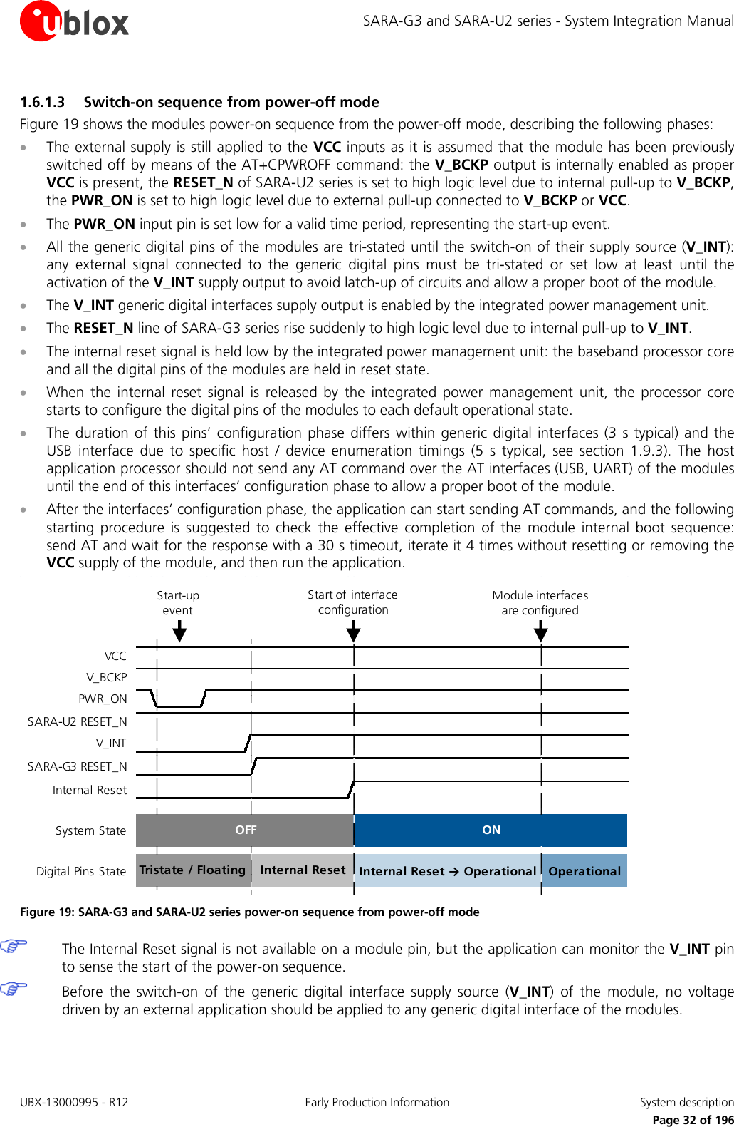
![SARA-G3 and SARA-U2 series - System Integration Manual 1.6.2 Module power-off 1.6.2.1 Switch-off events The SARA-G3 and SARA-U2 series modules can be properly switched off by: • AT+CPWROFF command (more details in u-blox AT Commands Manual [3]). The SARA-U2 series modules can be properly switched off also by: • Low pulse on the PWR_ON pin, which is normally set high by an external pull-up, for a valid time period (see the SARA-U2 series Data Sheet [2] for the detailed electrical characteristics of the PWR_ON input). In both the cases listed above, the current parameter settings are saved in the module’s non-volatile memory and a proper network detach is performed: these are the correct ways to switch off the modules. An abrupt under-voltage shutdown occurs on SARA-G3 and SARA-U2 series modules when the VCC module supply is removed, but in this case the current parameter settings are not saved in the module’s non-volatile memory and a proper network detach cannot be performed. It is highly recommended to avoid an abrupt removal of the VCC supply during SARA-G3 and SARA-U2 series modules normal operations: the power off procedure must be properly started by the appplication, as by the AT+CPWROFF command, waiting the command response for a proper time period (see u-blox AT Commands Manual [3]), and then a proper VCC supply must be held at least until the end of the modules’ internal power off sequence, which occurs when the generic digital interfaces supply output (V_INT) is switched off by the module. An abrupt hardware shutdown occurs on SARA-U2 modules when a low level is applied to the RESET_N input. In this case, the current parameter settings are not saved in the module’s non-volatile memory and a proper network detach is not performed. It is highly recommended to avoid an abrupt hardware shutdown of the module by forcing a low level on the RESET_N input pin during module normal operation: the RESET_N line should be set low only if reset or shutdown via AT commands fails or if the module does not reply to a specific AT command after a time period longer than the one defined in the u-blox AT Commands Manual [3]. An over-temperature or an under-temperature shutdown occurs on SARA-G3 and SARA-U2 series modules when the temperature measured within the cellular module reaches the dangerous area, if the optional Smart Temperature Supervisor feature is enabled and configured by the dedicated AT command. For more details see section 1.13.10 and to the u-blox AT Commands Manual [3], +USTS AT command. The Smart Temperature Supervisor feature is not supported by SARA-G300 and SARA-G310. UBX-13000995 - R12 Early Production Information System description Page 33 of 196](https://usermanual.wiki/u-blox/SARAU280/User-Guide-2520608-Page-33.png)
![SARA-G3 and SARA-U2 series - System Integration Manual 1.6.3 Module reset SARA-G3 and SARA-U2 series modules can be properly reset (rebooted) by: • AT+CFUN command (see the u-blox AT Commands Manual [3] for more details). This command causes an “internal” or “software” reset of the module, which is an asynchronous reset of the module baseband processor. The current parameter settings are saved in the module’s non-volatile memory and a proper network detach is performed: this is the proper way to reset the modules. An abrupt hardware reset occurs on SARA-G3 and SARA-U2 series modules when a low level is applied on the RESET_N input pin for a specific time period. In this case, the current parameter settings are not saved in the module’s non-volatile memory and a proper network detach is not performed. It is highly recommended to avoid an abrupt hardware reset of the module by forcing a low level on the RESET_N input during modules normal operation: the RESET_N line should be set low only if reset or shutdown via AT commands fails or if the module does not provide a reply to a specific AT command after a time period longer than the one defined in the u-blox AT Commands Manual [3]. As described in Figure 21, both the SARA-G3 and SARA-U2 series modules are equipped with an internal pull-up resistor which pulls the line to the high logic level when the RESET_N pin is not forced low from the external. The pull-up is internally biased by V_INT on SARA-G3 modules and is biased by V_BCKP on SARA-U2 modules. A series Schottky diode is mounted inside the SARA-G3 modules, increasing the RESET_N input voltage range. Refer to the SARA-G3 series Data Sheet [1] and the SARA-U2 series Data Sheet [2] for the detailed electrical characteristics of the RESET_N input. Baseband Processor18RESET_NSARA-U2 seriesResetPower ManagementReset10kV_BCKPBaseband Processor18RESET_NSARA-G3 seriesReset10kV_INT Figure 21: RESET_N input description When a low level is applied to the RESET_N input, it causes an “external” or “hardware” reset of the modules, with the following behavior of SARA-G3 and SARA-U2 series modules due to different internal circuits: • SARA-G3 modules: reset of the processor core, excluding the Power Management Unit and the RTC block. The V_INT generic digital interfaces supply is switched on and each digital pin is set in its internal reset state. The V_BCKP supply and the RTC block are switched on. • SARA-U2 modules: reset of the processor core and the Power Management Unit, excluding the RTC block. The V_INT generic digital interfaces supply is switched off and all digital pins are tri-stated (not supplied). The V_BCKP supply and the RTC block are switched on. Before the switch-on of the generic digital interface supply source (V_INT) of the module, no voltage driven by an external application should be applied to any generic digital interface of the modules. The internal reset state of all digital pins is reported in the pin description table in the SARA-G3 series Data Sheet [1] and in the SARA-U2 series Data Sheet [2]. UBX-13000995 - R12 Early Production Information System description Page 35 of 196](https://usermanual.wiki/u-blox/SARAU280/User-Guide-2520608-Page-35.png)
![SARA-G3 and SARA-U2 series - System Integration Manual 1.6.4 External 32 kHz signal input (EXT32K) The EXT32K pin is not available on SARA-G340, SARA-G350 and SARA-U2 series modules. The EXT32K pin of SARA-G300 / SARA-G310 modules is an input pin that must be fed by a proper 32 kHz signal to make available the reference clock for the Real Time Clock (RTC) timing, used by the module processor when in the low power idle-mode. SARA-G300 / SARA-G310 modules can enter the low power idle-mode only if a proper 32 kHz signal is provided at the EXT32K input pin, with power saving configuration enabled by the AT+UPSV command. In this way the different current consumption figures can be reached with the EXT32K input fed by the 32K_OUT output or by a proper external 32 kHz signal (for more details see section 1.5.1.4 and to “Current consumption” section in SARA-G3 series Data Sheet [1]). SARA-G300 / SARA-G310 modules can provide the RTC functions (as RTC timing by AT+CCLK command and RTC alarm by AT+CALA command) only if a proper 32 kHz signal is provided at the EXT32K input pin. The RTC functions will be available only when the module is switched on if the EXT32K input is fed by the 32K_OUT output, or they will be available also when the module is not powered or switched off if the EXT32K input is fed by a proper external 32 kHz signal. SARA-G3 series Data Sheet [1] describes the detailed electrical characteristics of the EXT32K input pin. The 32 kHz reference clock for the RTC timing is automatically generated by the internal oscillator provided on the SARA-G340, SARA-G350 and SARA-U2 series modules: the same pin (31) is a reserved (RSVD) pin internally not connected, since an external 32 kHz signal is not needed to enter the low power idle-mode and to provide the RTC functions. 1.6.5 Internal 32 kHz signal output (32K_OUT) The 32K_OUT pin is not available on SARA-G340, SARA-G350 and SARA-U2 series modules. The 32K_OUT pin of SARA-G300 / SARA-G310 modules is an output pin that provides a 32 kHz reference signal generated by the module, suitable only to feed the EXT32K input pin of SARA-G300 / SARA-G310 modules, to make available the reference clock for the Real Time Clock (RTC) timing, so that the modules can enter the low power idle-mode and can provide the RTC functions with modules switched on. The 32K_OUT pin does not provide the 32 kHz output signal when the SARA-G300 / SARA-G310 modules are in power down mode: the EXT32K input pin must be fed by an external proper 32 kHz signal to make available the RTC functions when the modules are not powered or switched off. SARA-G340, SARA-G350 and SARA-U2 series modules do not provide the 32K_OUT output, as there is no EXT32K input to feed on the modules: the pin 24 constitute the GPIO3 on these modules. UBX-13000995 - R12 Early Production Information System description Page 36 of 196](https://usermanual.wiki/u-blox/SARAU280/User-Guide-2520608-Page-36.png)
![SARA-G3 and SARA-U2 series - System Integration Manual 1.7 Antenna interface 1.7.1 Antenna RF interface (ANT) The ANT pin of SARA-G3 and SARA-U2 series modules represents the RF input/output for 2G or 3G cellular RF signals reception and transmission. The ANT pin has a nominal characteristic impedance of 50 Ω and must be connected to the antenna through a 50 Ω transmission line for proper RF signals reception and transmission. 1.7.1.1 Antenna RF interface requirements Table 10 summarizes the requirements for the antenna RF interface (ANT). See section 2.4.1 for suggestions to properly design an antenna circuit compliant to these requirements. The antenna circuit affects the RF compliance of the device integrating SARA-G3 and SARA-U2 series module with applicable required certification schemes. Compliance is guaranteed if the antenna RF interface (ANT) requirements summarized in Table 10 are fulfilled. Item Requirements Remarks Impedance 50 Ω nominal characteristic impedance The nominal characteristic impedance of the antenna RF connection must match the ANT pin 50 Ω impedance. Frequency Range See the SARA-G3 series Data Sheet [1] and the SARA-U2 series Data Sheet [2] The required frequency range of the antenna depends on the operating bands supported by the cellular module. Return Loss S11 < -10 dB (VSWR < 2:1) recommended S11 < -6 dB (VSWR < 3:1) acceptable The Return loss or the S11, as the VSWR, refers to the amount of reflected power, measuring how well the RF antenna connection matches the 50 Ω impedance. The impedance of the antenna RF termination must match as much as possible the 50 Ω impedance of the ANT pin over the operating frequency range, reducing as much as possible the amount of reflected power. Efficiency > -1.5 dB ( > 70% ) recommended > -3.0 dB ( > 50% ) acceptable The radiation efficiency is the ratio of the radiated power to the power delivered to antenna input: the efficiency is a measure of how well an antenna receives or transmits. The efficiency needs to be enough high over the operating frequency range to comply with the Over-The-Air radiated performance requirements, as Total Radiated Power and Total Isotropic Sensitivity, specified by certification schemes Maximum Gain See section 4.2.2 for maximum gain limits The power gain of an antenna is the radiation efficiency multiplied by the directivity: the maximum gain describes how much power is transmitted in the direction of peak radiation to that of an isotropic source. The maximum gain of the antenna connected to ANT pin must not exceed the values stated in section 4.2.2 to comply with regulatory agencies radiation exposure limits. Input Power > 2 W peak The antenna connected to ANT pin must support the maximum power transmitted by the modules. Detection Application board with antenna detection circuit If antenna detection is required by the custom application, proper antenna detection circuit must be implemented on the application board as described in section 2.4.2. Antenna assembly with built-in diagnostic circuit If antenna detection is required by the custom application, the external antenna assembly must be provided with proper diagnostic circuit as described in section 2.4.2. Table 10: Summary of antenna RF interface (ANT) requirements For the additional specific requirements applicable to the integration of SARA-G350 ATEX and SARA-U270 ATEX modules in applications intended for use in potentially explosive atmospheres, see section 2.14. UBX-13000995 - R12 Early Production Information System description Page 37 of 196](https://usermanual.wiki/u-blox/SARAU280/User-Guide-2520608-Page-37.png)
![SARA-G3 and SARA-U2 series - System Integration Manual 1.7.2 Antenna detection interface (ANT_DET) Antenna detection interface (ANT_DET) is not supported by SARA-G300 and SARA-G310 modules. The antenna detection is based on ADC measurement. The ANT_DET pin is an Analog to Digital Converter (ADC) provided to sense the antenna presence. The antenna detection function provided by ANT_DET pin is an optional feature that can be implemented if the application requires it. The antenna detection is forced by the +UANTR AT command. See the u-blox AT Commands Manual [3] for more details on this feature. The ANT_DET pin generates a DC current (20 µA for 5.4 ms on SARA-G340 / SARA-G350, 10 µA for 128 µs on SARA-U2 modules) and measures the resulting DC voltage, thus determining the resistance from the antenna connector provided on the application board to GND. So, the requirements to achieve antenna detection functionality are the following: • an RF antenna assembly with a built-in resistor (diagnostic circuit) must be used • an antenna detection circuit must be implemented on the application board See section 2.4.2 for antenna detection circuit on application board and diagnostic circuit on antenna assembly design-in guidelines. 1.8 SIM interface 1.8.1 (U)SIM card interface SARA-G3 and SARA-U2 series modules provide a high-speed SIM/ME interface, including automatic detection and configuration of the voltage required by the connected (U)SIM card or chip. Both 1.8 V and 3 V SIM types are supported: activation and deactivation with automatic voltage switch from 1.8 V to 3 V is implemented, according to ISO-IEC 7816-3 specifications. The VSIM supply output pin provides internal short circuit protection to limit start-up current and protect the device in short circuit situations. The SIM driver supports the PPS (Protocol and Parameter Selection) procedure for baud-rate selection, according to the values determined by the SIM Card. SIM Application Toolkit is supported by all SARA-G3 and SARA-U2 series except SARA-G300 and SARA-G310. 1.8.2 SIM card detection interface (SIM_DET) Not supported by SARA-G300-00S and SARA-G310-00S modules. The SIM_DET pin is configured as an external interrupt to detect the SIM card mechanical / physical presence. The pin is configured as input with an internal active pull-down enabled, and it can sense SIM card presence only if properly connected to the mechanical switch of a SIM card holder as described in section 2.5: • Low logic level at SIM_DET input pin is recognized as SIM card not present • High logic level at SIM_DET input pin is recognized as SIM card present The SIM card detection function provided by SIM_DET pin is an optional feature that can be implemented / used or not according to the application requirements: an Unsolicited Result Code (URC) is generated each time that there is a change of status (for more details see the u-blox AT Commands Manual [3], “simind” value of the <descr> parameter of the +CIND and +CMER commands. The optional function “SIM card hot insertion/removal” can be additionally enabled on the SARA-U2 modules’ SIM_DET pin by AT commands (see section 1.11 and u-blox AT Commands Manual [3], +UGPIOC, +UDCONF). UBX-13000995 - R12 Early Production Information System description Page 39 of 196](https://usermanual.wiki/u-blox/SARAU280/User-Guide-2520608-Page-39.png)
![SARA-G3 and SARA-U2 series - System Integration Manual 1.9 Serial interfaces SARA-G3 and SARA-U2 series modules provide the following serial communication interfaces: • UART interface: 9-wire unbalanced 1.8 V asynchronous serial interface available for AT commands, data communication, FW upgrades by means of the FOAT feature (see 1.9.1) • Auxiliary UART interface (not supported by SARA-U2 series): 3-wire unbalanced 1.8 V asynchronous serial interface available for FW upgrades by means of the u-blox EasyFlash tool and for diagnostic (see 1.9.2) • USB interface (not supported by SARA-G3 series): High-Speed USB 2.0 compliant interface available for AT commands, data communication, FW upgrades by means of the FOAT feature, FW upgrades by means of the u-blox EasyFlash tool and for diagnostic (see 1.9.3) • DDC interface (not supported by SARA-G300 / SARA-G310): I2C compatible 1.8 V interface available for the communication with u-blox positioning chips / modules and additionally, except for SARA-G3 series, with other external I2C devices as an audio codec (see 1.9.4) 1.9.1 Asynchronous serial interface (UART) 1.9.1.1 UART features The UART interface is a 9-wire 1.8 V unbalanced asynchronous serial interface available for AT commands and for packet-switched / circuit-switched data communication on all the SARA-G3 and SARA-U2 series modules. The UART interface provides RS-232 functionality conforming to the ITU-T V.24 Recommendation (more details available in ITU Recommendation [10]), with CMOS compatible signal levels: 0 V for low data bit or ON state, and 1.8 V for high data bit or OFF state. For detailed electrical characteristics see SARA-G3 series Data Sheet [1] and SARA-U2 series Data Sheet [2]. SARA-G3 and SARA-U2 series modules are designed to operate as a 2G or 3G cellular modem, which represents the Data Circuit-terminating Equipment (DCE) according to the ITU-T V.24 Recommendation [10]. The application processor connected to the module through the UART interface represents the Data Terminal Equipment (DTE). The signal names of SARA-G3 and SARA-U2 series modules’ UART interface conform to the ITU-T V.24 Recommendation [10]: e.g. the TXD line represents the data transmitted by the DTE (application processor data line output) and received by the DCE (module data line input). All flow control handshakes are supported by the UART interface and can be set by appropriate AT commands (see u-blox AT Commands Manual [3], &K, +IFC, \Q AT commands): hardware flow control (RTS/CTS), software flow control (XON/XOFF), or none flow control. Hardware flow control is enabled by default. SARA-G3 modules support the autobauding: the baud rate automatic detection is performed each time the DTE sends AT commands. After the detection the module works at the detected baud rate and the baud rate can be runtime changed by the DTE or by AT command (see u-blox AT Commands Manual [3], +IPR command). SARA-U2 modules support only the one-shot autobauding: the baud rate automatic detection is performed only once, at module start up. After the detection the module works at the detected baud rate and the baud rate can only be changed by AT command (see u-blox AT Commands Manual [3], +IPR command). SARA-G3 modules’ autobauding and SARA-U2 modules’ one-shot autobauding are enabled by default. UBX-13000995 - R12 Early Production Information System description Page 40 of 196](https://usermanual.wiki/u-blox/SARAU280/User-Guide-2520608-Page-40.png)
![SARA-G3 and SARA-U2 series - System Integration Manual The following baud rates can be configured by AT command (see u-blox AT Commands Manual [3], +IPR): • 1200 b/s • 2400 b/s • 4800 b/s • 9600 b/s • 19200 b/s • 38400 b/s • 57600 b/s • 115200 b/s, default value when the autobauding or the one-shot autobauding are disabled • 230400 b/s • 460800 b/s • 921600 b/s 460800 b/s and 921600 b/s baud rates are not supported by SARA-G3 series modules. 1200 b/s and 230400 b/s baud rates cannot be automatically detected by SARA-G3 series modules. 460800 b/s and 921600 b/s baud rates cannot be automatically detected by SARA-U2 series modules. SARA-G3 modules support the automatic frame recognition in conjunction with autobauding. SARA-U2 modules support the one-shot automatic frame recognition in conjunction with one-shot autobauding. SARA-G3 series modules’ automatic frame recognition and SARA-U2 series modules’ one-shot automatic frame recognition are enabled by default, as autobauding and one-shot autobauding. The following frame formats can be configured by AT command (see u-blox AT Commands Manual [3], +ICF): • 8N1 (8 data bits, No parity, 1 stop bit), default frame configuration with fixed baud rate • 8E1 (8 data bits, even parity, 1 stop bit) • 8O1 (8 data bits, odd parity, 1 stop bit) • 8N2 (8 data bits, No parity, 2 stop bits) • 7E1 (7 data bits, even parity, 1 stop bit) • 7O1 (7 data bits, odd parity, 1 stop bit) Figure 22 describes the 8N1 frame format, which is the default configuration with fixed baud rate. D0 D1 D2 D3 D4 D5 D6 D7Start of 1-BytetransferStart Bit(Always 0)Possible Start ofnext transferStop Bit(Always 1)tbit = 1/(Baudrate)Normal Transfer, 8N1 Figure 22: Description of UART default frame format (8N1) with fixed baud rate UBX-13000995 - R12 Early Production Information System description Page 41 of 196](https://usermanual.wiki/u-blox/SARAU280/User-Guide-2520608-Page-41.png)
![SARA-G3 and SARA-U2 series - System Integration Manual The module firmware can be updated over the UART interface by means of: • the Firmware upgrade Over AT (FOAT) feature, on all the SARA-G3 and SARA-U2 series modules • the u-blox EasyFlash tool, on SARA-U2 series modules only For more details on FW upgrade procedures see section 1.13 and Firmware update application note [25]. 1.9.1.2 UART AT interface configuration The UART interface of SARA-G3 and SARA-U2 series modules is available as AT command interface with the default configuration described in Table 11 (for more details and information about further settings, see the u-blox AT Commands Manual [3]). Interface AT Settings Comments UART interface AT interface: enabled AT command interface is enabled by default on the UART physical interface AT+IPR=0 Automatic baud rate detection enabled by default on SARA-G3 series One-shot automatic baud rate detection enabled by default on SARA-U2 series AT+ICF=0 Automatic frame format recognition enabled by default on SARA-G3 series One-shot automatic frame format recognition enabled by default on SARA-U2 series AT&K3 HW flow control enabled by default AT&S1 DSR line set ON in data mode8 and set OFF in command mode8 AT&D1 Upon an ON-to-OFF transition of DTR, the DCE enters online command mode8 and issues an OK result code AT&C1 Circuit 109 changes in accordance with the Carrier detect status; ON if the Carrier is detected, OFF otherwise MUX protocol: disabled Multiplexing mode is disabled by default and it can be enabled by AT+CMUX command. The following virtual channels are defined: • Channel 0: control channel • Channel 1: AT and Data • Channel 2: AT and Data • Channel 3: AT and Data (not available on SARA-G300 / SARA-G310 modules) • Channel 4: AT and Data (not available on SARA-G300 / SARA-G310 modules) • Channel 5: AT and Data (not available on SARA-G300 / SARA-G310 modules) • Channel 6: GNSS tunneling (not available on SARA-G300 / SARA-G310 modules) • Channel 7: SIM Access Profile (not available on SARA-G3 series modules) Table 11: Default UART AT interface configuration 8 Refer to the u-blox AT Commands Manual [3] for the definition of the interface data mode, command mode and online command mode. UBX-13000995 - R12 Early Production Information System description Page 42 of 196](https://usermanual.wiki/u-blox/SARAU280/User-Guide-2520608-Page-42.png)
![SARA-G3 and SARA-U2 series - System Integration Manual 1.9.1.3 UART signal behavior At the module switch-on, before the UART interface initialization (as described in the power-on sequence reported in Figure 18 or Figure 19), each pin is first tri-stated and then is set to its related internal reset state9. At the end of the boot sequence, the UART interface is initialized, the module is by default in active-mode, and the UART interface is enabled as AT commands interface. The configuration and the behavior of the UART signals after the boot sequence are described below. See section 1.4 for definition and description of module operating modes referred to in this section. RXD signal behavior The module data output line (RXD) is set by default to the OFF state (high level) at UART initialization. The module holds RXD in the OFF state until the module does not transmit some data. TXD signal behavior The module data input line (TXD) is set by default to the OFF state (high level) at UART initialization. The TXD line is then held by the module in the OFF state if the line is not activated by the DTE: an active pull-up is enabled inside the module on the TXD input. CTS signal behavior The module hardware flow control output (CTS line) is set to the ON state (low level) at UART initialization. If the hardware flow control is enabled, as it is by default, the CTS line indicates when the UART interface is enabled (data can be sent and received). The module drives the CTS line to the ON state or to the OFF state when it is either able or not able to accept data from the DTE over the UART (see 1.9.1.4 for more details). If hardware flow control is enabled, then when the CTS line is OFF it does not necessarily mean that the module is in low power idle-mode, but only that the UART is not enabled, as the module could be forced to stay in active-mode for other activities, e.g. related to the network or related to other interfaces. When the multiplexer protocol is active, the CTS line state is mapped to FCon / FCoff MUX command for flow control issues outside the power saving configuration while the physical CTS line is still used as a power state indicator. For more details, see Mux Implementation Application Note [23]. The CTS hardware flow control setting can be changed by AT commands (for more details, see u-blox AT Commands Manual [3], AT&K, AT\Q, AT+IFC AT command). If the hardware flow control is not enabled, the CTS line after the UART initialization behaves as following: • on SARA-U2 modules the CTS line is always held in the ON state • on SARA-G3 modules the CTS line is set in the ON or OFF state accordingly to the power saving state as illustrated in Figure 25 if AT+UPSV=2 is set, and the CTS line is held in the ON state otherwise When the power saving configuration is enabled and the hardware flow-control is not implemented in the DTE/DCE connection, data sent by the DTE can be lost: the first character sent when the module is in the low power idle-mode will not be a valid communication character (see 1.9.1.4 for more details). 9 Refer to the pin description table in the SARA-G3 series Data Sheet [1] and SARA-U2 series Data Sheet [2]. UBX-13000995 - R12 Early Production Information System description Page 43 of 196](https://usermanual.wiki/u-blox/SARAU280/User-Guide-2520608-Page-43.png)
![SARA-G3 and SARA-U2 series - System Integration Manual RTS signal behavior The hardware flow control input (RTS line) is set by default to the OFF state (high level) at UART initialization. The module then holds the RTS line in the OFF state if the line is not activated by the DTE: an active pull-up is enabled inside the module on the RTS input. If the HW flow control is enabled, as it is by default, the module monitors the RTS line to detect permission from the DTE to send data to the DTE itself. If the RTS line is set to the OFF state, any on-going data transmission from the module is interrupted until the subsequent RTS line change to the ON state. The DTE must still be able to accept a certain number of characters after the RTS line is set to the OFF state: the module guarantees the transmission interruption within two characters from RTS state change. Module behavior according to RTS hardware flow control status can be configured by AT commands (for more details, see u-blox AT Commands Manual [3], AT&K, AT\Q, AT+IFC command descriptions). If AT+UPSV=2 is set and HW flow control is disabled, the module monitors the RTS line to manage the power saving configuration: • When an OFF-to-ON transition occurs on the RTS input line, the UART is enabled and the module wakes up to active-mode: after ~20 ms from the OFF-to-ON transition the UART / module wake up is completed and data can be received without loss. The module cannot enter the low power idle-mode and the UART is kept enabled as long as the RTS input line is held in the ON state • If the RTS input line is set to the OFF state by the DTE, the UART is disabled (held in low power mode) and the module automatically enters low power idle-mode whenever possible For more details, see section 1.9.1.4 and u-blox AT Commands Manual [3], AT+UPSV command. DSR signal behavior If AT&S1 is set, as it is by default, the DSR module output line is set by default to the OFF state (high level) at UART initialization. The DSR line is then set to the OFF state when the module is in command mode or in online command mode and is set to the ON state when the module is in data mode (see the u-blox AT Commands Manual [3] for the definition of the interface data mode, command mode and online command mode). If AT&S0 is set, the DSR module output line is set by default to the ON state (low level) at UART initialization and is then always held in the ON state. DTR signal behavior The DTR module input line is set by default to the OFF state (high level) at UART initialization. The module then holds the DTR line in the OFF state if the line is not activated by the DTE: an active pull-up is enabled inside the module on the DTR input. Module behavior according to DTR status can be changed by AT command (for more details, see u-blox AT Commands Manual [3], AT&D command description). If AT+UPSV=3 is set, the DTR line is monitored by the module to manage the power saving configuration: • When an OFF-to-ON transition occurs on the DTR input line, the UART is enabled and the module wakes up to active-mode: after ~20 ms from the OFF-to-ON transition the UART / module wake up is completed and data can be received without loss. The module cannot enter the low power idle-mode and the UART is kept enabled as long as the DTR input line is held in the ON state • If the DTR input line is set to the OFF state by the DTE, the UART is disabled (held in low power mode) and the module automatically enters low power idle-mode whenever possible For more details, see section 1.9.1.4 and u-blox AT Commands Manual [3], AT+UPSV command. AT+UPSV=3 power saving configuration control by the DTR input is not supported by SARA-G3 modules. UBX-13000995 - R12 Early Production Information System description Page 44 of 196](https://usermanual.wiki/u-blox/SARAU280/User-Guide-2520608-Page-44.png)
![SARA-G3 and SARA-U2 series - System Integration Manual DCD signal behavior If AT&C1 is set, as it is by default, the DCD module output line is set by default to the OFF state (high level) at UART initialization. The module then sets the DCD line according to the carrier detect status: ON if the carrier is detected, OFF otherwise. For voice calls, DCD is set to the ON state when the call is established. For a data call there are the following scenarios (see the u-blox AT Commands Manual [3] for the definition of the interface data mode, command mode and online command mode): • Packet Switched Data call: Before activating the PPP protocol (data mode) a dial-up application must provide the ATD*99***<context_number># to the module: with this command the module switches from command mode to data mode and can accept PPP packets. The module sets the DCD line to the ON state, then answers with a CONNECT to confirm the ATD*99 command. The DCD ON is not related to the context activation but with the data mode • Circuit Switched Data call: To establish a data call, the DTE can send the ATD<number> command to the module which sets an outgoing data call to a remote modem (or another data module). Data can be transparent (non reliable) or non transparent (with the reliable RLP protocol). When the remote DCE accepts the data call, the module DCD line is set to ON and the CONNECT <communication baudrate> string is returned by the module. At this stage the DTE can send characters through the serial line to the data module which sends them through the network to the remote DCE attached to a remote DTE The DCD is set to ON during the execution of the +CMGS, +CMGW, +USOWR, +USODL AT commands requiring input data from the DTE: the DCD line is set to the ON state as soon as the switch to binary/text input mode is completed and the prompt is issued; DCD line is set to OFF as soon as the input mode is interrupted or completed (for more details see the u-blox AT Commands Manual [3]). The DCD line is kept in the ON state, even during the online command mode, to indicate that the data call is still established even if suspended, while if the module enters command mode, the DSR line is set to the OFF state. For more details see DSR signal behavior description. For scenarios when the DCD line setting is requested for different reasons (e.g. SMS texting during online command mode), the DCD line changes to guarantee the correct behavior for all the scenarios. For instance, in case of SMS texting in online command mode, if the data call is released, the DCD line is kept to ON till the SMS command execution is completed (even if the data call release would request the DCD setting to OFF). If AT&C0 is set, the DCD module output line is set by default to the ON state (low level) at UART initialization and is then always held in the ON state. UBX-13000995 - R12 Early Production Information System description Page 45 of 196](https://usermanual.wiki/u-blox/SARAU280/User-Guide-2520608-Page-45.png)
![SARA-G3 and SARA-U2 series - System Integration Manual RI signal behavior The RI module output line is set by default to the OFF state (high level) at UART initialization. Then, during an incoming call, the RI line is switched from the OFF state to the ON state with a 4:1 duty cycle and a 5 s period (ON for 1 s, OFF for 4 s, see Figure 23), until the DTE attached to the module sends the ATA string and the module accepts the incoming data call. The RING string sent by the module (DCE) to the serial port at constant time intervals is not correlated with the switch of the RI line to the ON state. Figure 23: RI behavior during an incoming call The RI line can notify an SMS arrival. When the SMS arrives, the RI line switches from OFF to ON for 1 s (see Figure 24), if the feature is enabled by the AT+CNMI command (see the u-blox AT Commands Manual [3]). Figure 24: RI behavior at SMS arrival This behavior allows the DTE to stay in power saving mode until the DCE related event requests service. For SMS arrival, if several events coincidently occur or in quick succession each event independently triggers the RI line, although the line will not be deactivated between each event. As a result, the RI line may stay to ON for more than 1 s. If an incoming call is answered within less than 1 s (with ATA or if auto-answering is set to ATS0=1) than the RI line is set to OFF earlier. As a result: RI line monitoring cannot be used by the DTE to determine the number of received SMSes. For multiple events (incoming call plus SMS received), the RI line cannot be used to discriminate the two events, but the DTE must rely on the subsequent URCs and interrogate the DCE with proper commands. The RI line can additionally notify all the URCs and all the incoming data (PPP, Direct Link, sockets, FTP), if the feature is enabled by the AT+URING command (for more details see u-blox AT Commands Manual [3]): the RI line is asserted when one of the configured events occur and it remains asserted for 1 s unless another configured event will happen, with the same behavior described in Figure 24. The AT+URING command for the notification of all the URCs and all the incoming data (PPP, Direct Link, sockets, FTP) over the RI line output is not supported by SARA-G3 modules. SMS arrives time [s] 0 RI ON RI OFF 1s SMS time [s] 0 RI ON RI OFF 1s 1stime [s]151050RI ONRI OFFCall incomes1stime [s]151050RI ONRI OFFCall incomesUBX-13000995 - R12 Early Production Information System description Page 46 of 196](https://usermanual.wiki/u-blox/SARAU280/User-Guide-2520608-Page-46.png)
![SARA-G3 and SARA-U2 series - System Integration Manual 1.9.1.4 UART and power-saving The power saving configuration is controlled by the AT+UPSV command (for the complete description, see u-blox AT Commands Manual [3]). When power saving is enabled, the module automatically enters low power idle-mode whenever possible, and otherwise the active-mode is maintained by the module (see section 1.4 for definition and description of module operating modes referred to in this section). The AT+UPSV command configures both the module power saving and also the UART behavior in relation to the power saving. The conditions for the module entering idle-mode also depend on the UART power saving configuration. Three different power saving configurations can be set by the AT+UPSV command: • AT+UPSV=0, power saving disabled: module forced on active-mode and UART interface enabled (default) • AT+UPSV=1, power saving enabled: module cyclic active / idle-mode and UART enabled / disabled • AT+UPSV=2, power saving enabled and controlled by the UART RTS input line • AT+UPSV=3, power saving enabled and controlled by the UART DTR input line The AT+UPSV=3 power saving configuration is not supported by SARA-G3 modules. The different power saving configurations that can be set by the +UPSV AT command are described in details in the following subsections. Table 12 summarizes the UART interface communication process in the different power saving configurations, in relation with HW flow control settings and RTS input line status. For more details on the +UPSV AT command description, refer to u-blox AT commands Manual [3]. AT+UPSV HW flow control RTS line DTR line Communication during idle-mode and wake up 0 Enabled (AT&K3) ON ON or OFF Data sent by the DTE are correctly received by the module. Data sent by the module is correctly received by the DTE. 0 Enabled (AT&K3) OFF ON or OFF Data sent by the DTE should be buffered by the DTE and will be correctly received by the module when RTS is set to ON. Data sent by the module is buffered by the module and will be correctly received by the DTE when it is ready to receive data (i.e. RTS line will be ON). 0 Disabled (AT&K0) ON or OFF ON or OFF Data sent by the DTE is correctly received by the module. Data sent by the module is correctly received by the DTE if it is ready to receive data, otherwise data is lost. 1 Enabled (AT&K3) ON ON or OFF Data sent by the DTE should be buffered by the DTE and will be correctly received by the module when active-mode is entered. Data sent by the module is correctly received by the DTE. 1 Enabled (AT&K3) OFF ON or OFF Data sent by the DTE should be buffered by the DTE and will be correctly received by the module when active-mode is entered. Data sent by the module is buffered by the module and will be correctly received by the DTE when it is ready to receive data (i.e. RTS line will be ON). 1 Disabled (AT&K0) ON or OFF ON or OFF The first character sent by the DTE is lost, but after ~20 ms the UART and the module are waked up: recognition of subsequent characters is guaranteed after the complete UART / module wake-up. Data sent by the module is correctly received by the DTE if it is ready to receive data, otherwise data is lost. 2 Enabled (AT&K3) ON or OFF ON or OFF Not Applicable: HW flow control cannot be enabled with AT+UPSV=2. 2 Disabled (AT&K0) ON ON or OFF Data sent by the DTE is correctly received by the module. Data sent by the module is correctly received by the DTE if it is ready to receive data, otherwise data is lost. 2 Disabled (AT&K0) OFF ON or OFF Data sent by the DTE is lost by SARA-U2 modules. The first character sent by the DTE is lost by SARA-G3 modules, but after ~20 ms the UART and the module are waked up: recognition of subsequent characters is guaranteed after the complete UART / module wake-up. Data sent by the module is correctly received by the DTE if it is ready to receive data, otherwise data is lost. UBX-13000995 - R12 Early Production Information System description Page 47 of 196](https://usermanual.wiki/u-blox/SARAU280/User-Guide-2520608-Page-47.png)
![SARA-G3 and SARA-U2 series - System Integration Manual AT+UPSV HW flow control RTS line DTR line Communication during idle-mode and wake up 3 Enabled (AT&K3) ON ON Data sent by the DTE is correctly received by the module. Data sent by the module is correctly received by the DTE. 3 Enabled (AT&K3) ON OFF Data sent by the DTE is lost by the module. Data sent by the module is correctly received by the DTE. 3 Enabled (AT&K3) OFF ON Data sent by the DTE is correctly received by the module. Data sent by the module is buffered by the module and will be correctly received by the DTE when it is ready to receive data (i.e. RTS line will be ON). 3 Enabled (AT&K3) OFF OFF Data sent by the DTE is lost by the module. Data sent by the module is buffered by the module and will be correctly received by the DTE when it is ready to receive data (i.e. RTS line will be ON). 3 Disabled (AT&K0) ON or OFF ON Data sent by the DTE is correctly received by the module. Data sent by the module is correctly received by the DTE if it is ready to receive data, otherwise data are lost. 3 Disabled (AT&K0) ON or OFF OFF Data sent by the DTE is lost by the module. Data sent by the module is correctly received by the DTE if it is ready to receive data, otherwise data are lost. Table 12: UART and power-saving summary AT+UPSV=0: power saving disabled, fixed active-mode The module does not enter idle-mode and the UART interface is enabled (data can be sent and received): the CTS line is always held in the ON state after UART initialization. This is the default configuration. AT+UPSV=1: power saving enabled, cyclic idle/active-mode On SARA-G3 modules, when the AT+UPSV=1 command is issued by the DTE, the UART is disabled after the timeout set by the second parameter of the +UPSV AT command (for more details see u-blox AT commands Manual [3]). On SARA-U2 modules, when the AT+UPSV=1 command is issued by the DTE, the UART is immediately disabled. Afterwards, the UART of SARA-G3 and SARA-U2 series modules is periodically enabled to receive or send data and, if data has not been received or sent over the UART, the interface is automatically disabled whenever possible according to the timeout configured by the second parameter of the +UPSV AT command. The module automatically enters the low power idle-mode whenever possible but it wakes up to active-mode according to the UART periodic wake up so that the module cyclically enters the low power idle-mode and the active-mode. Additionally, the module wakes up to active-mode according to any required activity related to the network or any other required activity related to the functions / interfaces of the module. The UART is enabled, and the module does not enter low power idle-mode, in the following cases: • During the periodic UART wake up to receive or send data • If the module needs to transmit some data over the UART (e.g. URC) • On SARA-G3 modules, during a CSD data call and a PSD data call with external context activation • On SARA-G3 modules, during a voice call • If a character is sent by the DTE with HW flow control disabled, the first character sent causes the system wake-up due to the “wake up via data reception” feature described in the following subsection, and the UART will be then kept enabled after the last data received according to the timeout set by the second parameter of the AT+UPSV=1 command The module, outside an active call, periodically wakes up from idle-mode to active-mode to monitor the paging channel of the current base station (paging block reception), according to 2G or 3G discontinuous reception (DRX) specification. UBX-13000995 - R12 Early Production Information System description Page 48 of 196](https://usermanual.wiki/u-blox/SARAU280/User-Guide-2520608-Page-48.png)
![SARA-G3 and SARA-U2 series - System Integration Manual The time period between two paging receptions is defined by the current base station (i.e. by the network): • If the module is registered with a 2G network, the paging reception period can vary from ~0.47 s (DRX = 2, i.e. 2 x 51 2G-frames) up to ~2.12 s (DRX = 9, i.e. 9 x 51 2G-frames) • If the module is registered with a 3G network, the paging reception period can vary from 0.64 s (DRX = 6, i.e. 26 3G-frames) up to 5.12 s (DRX = 9, i.e. 29 3G-frames) The time period of the UART enable/disable cycle is configured differently when the module is registered with a 2G network compared to when the module is registered with a 3G network: • 2G: the UART is synchronously enabled to every paging reception on SARA-G3 modules, whereas the UART is not necessarily enabled at every paging reception on SARA-U2 modules: the UART is enabled concurrently to a paging reception, and then, as data has not been received or sent, the UART is disabled until the first paging reception that occurs after a timeout of 2.0 s, and therefore the interface is enabled again • 3G: the UART is asynchronously enabled to paging receptions, as the UART is enabled for ~20 ms, and then, if data are not received or sent, the UART is disabled for 2.5 s, and afterwards the interface is enabled again • Not registered: when a module is not registered with a network, the UART is enabled for ~20 ms, and then, if data has not been received or sent, the UART is disabled for ~2.1 s on SARA-G3 modules or for 2.5 s on SARA-U2 modules, and afterwards the interface is enabled again The module active-mode duration outside an active call depends on: • Network parameters, related to the time interval for the paging block reception (minimum of ~11 ms) • Duration of UART enable time in absence of data reception (~20 ms) • The time period from the last data received at the serial port during the active-mode: the module does not enter idle-mode until a timeout expires. The second parameter of the +UPSV AT command configures this timeout, from 40 2G-frames (i.e. 40 x 4.615 ms = 184 ms) up to 65000 2G-frames (i.e. 65000 x 4.615 ms = 300 s). Default value is 2000 2G-frames (i.e. 2000 x 4.615 ms = 9.2 s) The active-mode duration can be extended indefinitely since every subsequent character received during the active-mode, resets and restarts the timer. The timeout is ignored only by SARA-U2 modules immediately after AT+UPSV=1 has been sent, so that the UART interface is disabled and the module may enter idle-mode immediately after the AT+UPSV=1 is sent The hardware flow-control output (CTS line) indicates when the UART interface is enabled (data can be sent and received over the UART), if HW flow control is enabled, as illustrated in Figure 25. time [s]CTS ONCTS OFFUART disabled~10 ms (min)UART enabled~9.2 s (default)UART enabledData input0.47-2.10 s Figure 25: CTS behavior with power saving enabled (AT+UPSV=1) and HW flow control enabled: the CTS output line indicates when the UART interface of the module is enabled (CTS = ON = low level) or disabled (CTS = OFF = high level) UBX-13000995 - R12 Early Production Information System description Page 49 of 196](https://usermanual.wiki/u-blox/SARAU280/User-Guide-2520608-Page-49.png)
![SARA-G3 and SARA-U2 series - System Integration Manual AT+UPSV=2: power saving enabled and controlled by the RTS line This configuration can only be enabled with the module hardware flow control disabled by AT&K0 command. The UART interface is immediately disabled after the DTE sets the RTS line to OFF. Then, the module automatically enters idle-mode whenever possible according to any required activity related to the network or any other required activity related to the functions / interfaces of the module. The UART is disabled as long as the RTS line is held to OFF, but the UART is enabled in the following cases: • If the module needs to transmit some data over the UART (e.g. URC) • On SARA-G3 modules, during a CSD data call and a PSD data call with external context activation • On SARA-G3 modules, during a voice call • On SARA-G3 modules, if a data is sent by the DTE, it causes the system wake-up due to the “wake up via data reception” feature described in the following subsection, and the UART will be then kept enabled after the last data received according to the timeout previously set with the AT+UPSV=1 configuration When an OFF-to-ON transition occurs on the RTS input line, the UART is re-enabled and the module, if it was in idle-mode, switches from idle to active-mode after ~20 ms: this is the UART and module “wake up time”. If the RTS line is set to ON by the DTE the module is not allowed to enter the low power idle-mode and the UART is kept enabled. On SARA-G3 modules, the CTS output line indicates the power saving state as illustrated in Figure 25, even with AT+UPSV=2. AT+UPSV=3: power saving enabled and controlled by the DTR line The AT+UPSV=3 power saving configuration is not supported by SARA-G3 modules. The AT+UPSV=3 configuration can be enabled regardless the flow control setting on UART. In particular, the HW flow control can be enabled (AT&K3) or disabled (AT&K0) on UART during this configuration. The UART interface is immediately disabled after the DTE sets the DTR line to OFF. Then, the module automatically enters idle-mode whenever possible according to any required activity related to the network or any other required activity related to the functions / interfaces of the module. The UART is disabled as long as the DTR line is set to OFF, but the UART is enabled in the following cases: • If the module needs to transmit some data over the UART (e.g. URC) When an OFF-to-ON transition occurs on the DTR input line, the UART is re-enabled and the module, if it was in idle-mode, switches from idle to active mode after 20 ms: this is the UART and module “wake up time”. If the DTR line is set to ON by the DTE, the module is not allowed to enter idle-mode and the UART is kept enabled until the DTR line is set to OFF. When the AT+UPSV=3 configuration is enabled, the DTR input line can still be used by the DTE to control the module behavior according to AT&D command configuration (see u-blox AT Commands Manual [3]). The CTS output line indicates the UART power saving state as illustrated in Figure 25, if HW flow control is enabled with AT+UPSV=3. UBX-13000995 - R12 Early Production Information System description Page 50 of 196](https://usermanual.wiki/u-blox/SARAU280/User-Guide-2520608-Page-50.png)
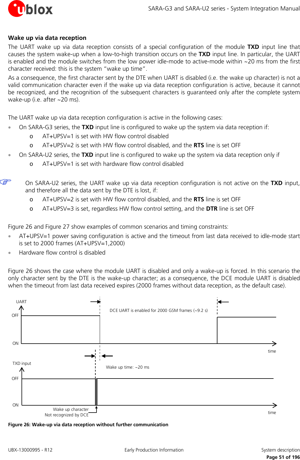
![SARA-G3 and SARA-U2 series - System Integration Manual Figure 27 shows the case where in addition to the wake-up character further (valid) characters are sent. The wake up character wakes-up the module UART. The other characters must be sent after the “wake up time” of ~20 ms. If this condition is satisfied, the module (DCE) recognizes characters. The module will disable the UART after 2000 GSM frames from the latest data reception. DCE UART is enabled for 2000 GSM frames (~9.2s) after the last data receivedtime Wake up time: ~20 mstime Wake up character Not recognized by DCEValid characters Recognized by DCEOFFONTXD inputUARTOFFON Figure 27: Wake-up via data reception with further communication The “wake-up via data reception” feature cannot be disabled. In command mode10, if autobauding is enabled and the DTE does not implement HW flow control, the DTE must always send a character to the module before the “AT” prefix set at the beginning of each command line: the first character is ignored if the module is in active-mode, or it represents the wake-up character if the module is in idle-mode. In command mode10, if autobauding is disabled, the DTE must always send a dummy “AT” before each command line: the first character is not ignored if the module is in active-mode (i.e. the module replies “OK”), or it represents the wake up character if the module is in low power idle-mode (i.e. the module does not reply). No wake-up character or dummy “AT” is required from the DTE during a voice or data call since the module UART interface continues to be enabled and does not need to be woken-up. Furthermore in data mode10 a dummy “AT” would affect the data communication. Additional considerations for SARA-U2 modules SARA-U2 modules are forced to stay in active-mode if the USB is connected and not suspended, and therefore the AT+UPSV=1, AT+UPSV=2 or AT+UPSV=3 settings are overruled but they have effect on the UART behavior: they configure UART interface power saving, so that UART is enabled / disabled according to the AT+UPSV=1, AT+UPSV=2 or AT+UPSV=3 settings. To set the AT+UPSV=1, AT+UPSV=2 or AT+UPSV=3 configuration over the USB interface of SARA-U2 modules, the autobauding must be previously disabled on the UART by the +IPR AT command over the used AT interface (the USB), and this +IPR AT command configuration must be saved in the module’ non-volatile memory (see u-blox AT Commands Manual [3]). Then, after the subsequent module re-boot, AT+UPSV=1, AT+UPSV=2 or AT+UPSV=3 can be issued over the used AT interface (the USB): all the AT profiles are updated accordingly. 10 Refer to the u-blox AT Commands Manual [3] for the definition of the interface data mode, command mode and online command mode. UBX-13000995 - R12 Early Production Information System description Page 52 of 196](https://usermanual.wiki/u-blox/SARAU280/User-Guide-2520608-Page-52.png)
![SARA-G3 and SARA-U2 series - System Integration Manual 1.9.1.5 Multiplexer protocol (3GPP 27.010) SARA-G3 and SARA-U2 series modules have a software layer with MUX functionality, the 3GPP TS 27.010 Multiplexer Protocol [13], available on the UART physical link. The auxiliary UART, the USB and the DDC (I2C) serial interfaces do not support the multiplexer protocol. This is a data link protocol (layer 2 of OSI model) which uses HDLC-like framing and operates between the module (DCE) and the application processor (DTE) and allows a number of simultaneous sessions over the used physical link (UART or SPI): the user can concurrently use AT command interface on one MUX channel and Packet-Switched / Circuit-Switched Data communication on another multiplexer channel. Each session consists of a stream of bytes transferring various kinds of data such as SMS, CBS, PSD, GNSS, AT commands in general. This permits, for example, SMS to be transferred to the DTE when a data connection is in progress. The following virtual channels are defined: • Channel 0: control channel • Channel 1: AT and Data • Channel 2: AT and Data • Channel 3: AT and Data (not available on SARA-G300 / SARA-G310 modules) • Channel 4: AT and Data (not available on SARA-G300 / SARA-G310 modules) • Channel 5: AT and Data (not available on SARA-G300 / SARA-G310 modules) • Channel 6: GNSS tunneling (not available on SARA-G300 / SARA-G310 modules) • Channel 7: SIM Access Profile (not available on SARA-G3 series modules) For more details, refer to Mux implementation Application Note [23]. 1.9.2 Auxiliary asynchronous serial interface (UART AUX) The auxiliary UART interface is not available on SARA-U2 series modules. SARA-G3 modules provide the auxiliary UART interface: it is a 3-wire unbalanced 1.8 V asynchronous serial interface (only the RXD_AUX data output and TXD_AUX data input are provided), available for module FW upgrade by means of the u-blox EasyFlash tool and for diagnostic purpose. The AT commands interface is not available on the auxiliary UART interface. 1.9.3 USB interface The USB interface is not available on SARA-G3 series modules. 1.9.3.1 USB features SARA-U2 modules include a High-Speed USB 2.0 compliant interface with maximum data rate of 480 Mb/s between the module and a host processor. The module itself acts as a USB device and can be connected to any USB host such as a Personal Computer or an embedded application microprocessor for AT commands, data communication, FW upgrade by means of the FOAT feature, FW upgrade by means of the u-blox EasyFlash tool and for diagnostic purpose. The USB_D+/USB_D- pins carry USB serial data and signaling while the VUSB_DET input pin senses the VBUS USB supply presence (nominally +5 V at the source) to detect the host connection and enable the interface. The USB interface of the module is enabled only if a valid voltage is detected by the VUSB_DET input (see the SARA-U2 series Data Sheet [2]). Neither the USB interface, nor the whole module is supplied by the VUSB_DET input: the VUSB_DET senses the USB supply voltage and absorbs few microamperes. UBX-13000995 - R12 Early Production Information System description Page 53 of 196](https://usermanual.wiki/u-blox/SARAU280/User-Guide-2520608-Page-53.png)
![SARA-G3 and SARA-U2 series - System Integration Manual SARA-U2 modules provide by default the following USB profile with the listed set of available USB functions (USB CDCs, Communications Device Classes): • USB1: AT and Data (AT command interface and packet-switched / circuit-switched data communication) • USB2: AT and Data (AT command interface and packet-switched / circuit-switched data communication) • USB3: AT and Data (AT command interface and packet-switched / circuit-switched data communication) • USB4: GPS (tunneling communication with the u-blox GNSS receiver connected over I2C interface) • USB5: Primary Log (diagnostic purpose) • USB6: Secondary Log (diagnostic purpose) • USB7: SAP (SIM Access Profile) The user can concurrently use the AT command interface on one CDC, and packet-switched / circuit-switched data communication on another CDC. The module firmware can be upgraded over the USB interface using the u-blox EasyFlash tool or by means of AT command (for more details see section 1.13.13 and Firmware update application note [25]). For more details on the configuration of the USB interface of SARA-U2 modules, see the u-blox AT Commands Manual [3], +UUSBCONF AT command. USB CDC/ACM drivers are available for the following operating system platforms: • Windows 2000 • Windows XP • Windows Vista • Windows 7 • Windows 8 • Windows CE 5.0 • Windows Embedded CE 6.0 • Windows Embedded Compact 7 • Windows Embedded Automotive 7 • Windows Mobile 5 • Windows Mobile 6 • Windows Mobile 6.1 • Windows Mobile 6.5 SARA-U2 modules are compatible with standard Linux/Android USB kernel drivers. The USB profile of SARA-U2 module identifies itself by its VID (Vendor ID) and PID (Product ID) combination, included in the USB device descriptor according to the USB 2.0 specifications [14]. VID and PID of the SARA-U2 module USB profile with the set of USB functions described in details above (AT and Data, GNSS tunneling, Diagnostic, SAP) are the following: • VID = 0x1546 • PID = 0x1102 If the USB interface of a SARA-U2 module is connected to the host before the module switch on, or if the module is reset with the USB interface connected to the host, the VID and PID are automatically updated runtime, after the USB detection. First, VID and PID are the following: • VID = 0x058B • PID = 0x0041 UBX-13000995 - R12 Early Production Information System description Page 54 of 196](https://usermanual.wiki/u-blox/SARAU280/User-Guide-2520608-Page-54.png)
![SARA-G3 and SARA-U2 series - System Integration Manual This VID and PID combination identifies a USB profile where the set of USB functions described in details above (AT and Data, GNSS tunneling, Diagnostic, SAP) are not available: AT commands must not be sent to the module over the USB profile identified by this VID and PID combination. Then, after a time period (roughly 5 s, depending on the host / device enumeration timings), the VID and PID are updated to the following ones, which are related to the SARA-U2 module USB profile with the set of USB functions described in details above (AT and Data, GNSS tunneling, Diagnostic, SAP): • VID = 0x1546 • PID = 0x1102 1.9.3.2 USB and power saving If power saving is enabled by the AT+UPSV command, the modules automatically enter the USB suspended state when the device has observed no bus traffic for a specified time period (see the USB 2.0 specifications [14]). In suspended state, the module maintains any USB internal status as device. In addition, the module enters the suspended state when the hub port it is attached to is disabled. This is referred to as USB selective suspend. The module exits suspend mode when there is bus activity. If the USB is connected and not suspended, the module is forced to stay in active-mode, therefore the AT+UPSV settings are overruled but they have effect on the power saving configuration of the other interfaces. The modules are capable of USB remote wake-up signaling: i.e. it may request the host to exit suspend mode or selective suspend by using electrical signaling to indicate remote wake-up. This notifies the host that it should resume from its suspended mode, if necessary, and service the external event. Remote wake-up is accomplished using electrical signaling described in the USB 2.0 specifications [14]. For the module current consumption description with power saving enabled and USB suspended, or with power saving disabled and USB not suspended, see sections 1.5.1.4, 1.5.1.5 and SARA-U2 series Data Sheet [2]. 1.9.4 DDC (I2C) interface SARA-G300 and SARA-G310 modules do not support DDC (I2C) interface. An I2C bus compatible Display Data Channel (DDC) interface for communication with u-blox GNSS receivers is available on SDA and SCL pins of SARA-G340, SARA-G350 and SARA-U2 modules. Only this interface provides the communication between the u-blox cellular module and u-blox positioning chips and modules. SARA-U2 modules additionally support the communication with other external I2C devices as an audio codec. The AT commands interface is not available on the DDC (I2C) interface. DDC (I2C) slave-mode operation is not supported: the cellular module can act as master only, and the connected u-blox GNSS receiver or any other external I2C devices acts as slave in the DDC (I2C) communication. Two lines, serial data (SDA) and serial clock (SCL), carry information on the bus. SCL is used to synchronize data transfers, and SDA is the data line. To be compliant to the I2C bus specifications, the module interface pins are open drain output and pull up resistors must be externally provided conforming to the I2C bus specifications [15]. u-blox has implemented special features in SARA-G340, SARA-G350 and SARA-U2 modules to ease the design effort required for the integration of a u-blox cellular module with a u blox GNSS receiver. Combining a u-blox cellular module with a u-blox GNSS receiver allows designers to have full access to the positioning receiver directly via the cellular module: it relays control messages to the GNSS receiver via a dedicated DDC (I2C) interface. A 2nd interface connected to the positioning receiver is not necessary: AT commands via the UART or USB serial interface of the cellular module allows a fully control of the GNSS receiver from any host processor. UBX-13000995 - R12 Early Production Information System description Page 55 of 196](https://usermanual.wiki/u-blox/SARAU280/User-Guide-2520608-Page-55.png)
![SARA-G3 and SARA-U2 series - System Integration Manual SARA-G340, SARA-G350 and SARA-U2 modules feature embedded GNSS aiding that is a set of specific features developed by u-blox to enhance GNSS performance, decreasing the Time To First Fix (TTFF), thus allowing to calculate the position in a shorter time with higher accuracy. SARA-G340, SARA-G350 and SARA-U2 modules support these GNSS aiding types: • Local aiding • AssistNow Online • AssistNow Offline • AssistNow Autonomous The embedded GNSS aiding features can be used only if the DDC (I2C) interface of the cellular module is connected to the u-blox GNSS receivers. SARA-G340, SARA-G350 and SARA-U2 cellular modules provide additional custom functions over GPIO pins to improve the integration with u-blox positioning chips and modules. GPIO pins can handle: • GNSS receiver power-on/off: “GNSS supply enable” function provided by GPIO2 improves the positioning receiver power consumption. When the GNSS functionality is not required, the positioning receiver can be completely switched off by the cellular module that is controlled by AT commands • The wake up from idle-mode when the GNSS receiver is ready to send data: “GNSS data ready” function provided by GPIO3 improves the cellular module power consumption. When power saving is enabled in the cellular module by the AT+UPSV command and the GNSS receiver does not send data by the DDC (I2C) interface, the module automatically enters idle-mode whenever possible. With the “GNSS data ready” function the GNSS receiver can indicate to the cellular module that it is ready to send data by the DDC (I2C) interface: the positioning receiver can wake up the cellular module if it is in idle-mode, so the cellular module does not lose the data sent by the GNSS receiver even if power saving is enabled • The RTC synchronization signal to the GNSS receiver: “GNSS RTC sharing” function provided by GPIO4 improves GNSS receiver performance, decreasing the Time To First Fix (TTFF), and thus allowing to calculate the position in a shorter time with higher accuracy. When GPS local aiding is enabled, the cellular module automatically uploads data such as position, time, ephemeris, almanac, health and ionospheric parameter from the positioning receiver into its local memory, and restores this to the GNSS receiver at the next power up of the positioning receiver For more details regarding the handling of the DDC (I2C) interface, the GNSS aiding features and the GNSS related functions over GPIOs, see section 1.11, to the u-blox AT Commands Manual [3] (AT+UGPS, AT+UGPRF, AT+UGPIOC AT commands) and the GNSS Implementation Application Note [24]. “GNSS data ready” and “GNSS RTC sharing” functions are not supported by all u-blox GNSS receivers HW or ROM/FW versions. See the GNSS Implementation Application Note [24] or to the Hardware Integration Manual of the u-blox GNSS receivers for the supported features. As additional improvement for the GNSS receiver performance, the V_BCKP supply output of SARA-G340, SARA-G350 and SARA-U2 modules can be connected to the V_BCKP supply input pin of u-blox positioning chips and modules to provide the supply for the GNSS real time clock and backup RAM when the VCC supply of the cellular module is within its operating range and the VCC supply of the GNSS receiver is disabled. This enables the u-blox positioning receiver to recover from a power breakdown with either a hot start or a warm start (depending on the duration of the GNSS receiver VCC outage) and to maintain the configuration settings saved in the backup RAM. UBX-13000995 - R12 Early Production Information System description Page 56 of 196](https://usermanual.wiki/u-blox/SARAU280/User-Guide-2520608-Page-56.png)
![SARA-G3 and SARA-U2 series - System Integration Manual 1.10 Audio interface SARA-G300 and SARA-G310 modules do not support audio interface. The following audio interfaces are provided by SARA-G3 and SARA-U2 series modules: • SARA-G340 and SARA-G350 modules provide one analog audio interface and one digital audio interface • SARA-U2 modules provide one digital audio interface The audio interfaces can be selected and set by the dedicated AT command +USPM (refer to the u-blox AT Commands Manual [3]): this command allows setting the audio path mode, composed by the uplink audio path and the downlink audio path. Each uplink path mode defines the physical input (i.e. the analog or the digital audio input) and the set of parameters to process the uplink audio signal (uplink gains, uplink digital filters, echo canceller parameters). For example the “Headset microphone” uplink path uses the differential analog audio input with the default parameters for the headset profile. Each downlink path mode defines the physical output (i.e. the analog or the digital audio output) and the set of parameters to process the downlink audio signal (downlink gains, downlink digital filters and sidetone). For example the “Mono headset” downlink path uses the differential analog audio output with the default parameters for the headset profile. The set of parameters to process the uplink or the downlink audio signal can be changed with dedicated AT commands for each uplink or downlink path and then stored in two profiles in the non volatile memory (refer to u-blox AT Commands Manual [3] for Audio parameters tuning commands). 1.10.1 Analog audio interface SARA-U2 modules do not provide analog audio interface. 1.10.1.1 Uplink path SARA-G340 / SARA-G350 pins related to the analog audio uplink path are: • MIC_P / MIC_N: Differential analog audio signal inputs (positive/negative). These two pins are internally directly connected to the differential input of an integrated Low Noise Amplifier, without any internal series capacitor for DC blocking. The LNA output is internally connected to the digital processing system by an integrated sigma-delta analog-to-digital converter • MIC_BIAS: Supply output for an external microphone. The pin is internally connected to the output of a low noise LDO linear regulator provided with proper internal bypass capacitor to guarantee stable operation of the linear regulator • MIC_GND: Local ground for the external microphone. The pin is internally connected to ground as a sense line as the reference for the analog audio input The analog audio input is selected when the parameter <main_uplink> in AT+USPM command is set to “Headset microphone”, “Handset microphone” or “Hands-free microphone”: the uplink analog path profiles use the same physical input but have different sets of audio parameters (for more details, refer to u-blox AT Commands Manual [3], AT+USPM, AT+UMGC, AT+UUBF, AT+UHFP commands). SARA-G3 series Data Sheet [1] provides the detailed electrical characteristics of the analog audio uplink path. UBX-13000995 - R12 Early Production Information System description Page 57 of 196](https://usermanual.wiki/u-blox/SARAU280/User-Guide-2520608-Page-57.png)
![SARA-G3 and SARA-U2 series - System Integration Manual 1.10.1.2 Downlink path SARA-G340 / SARA-G350 pins related to the analog audio downlink path are: • SPK_P / SPK_N: Differential analog audio signal output (positive/negative). These two pins are directly connected internally to the differential output of a low power audio amplifier, for which the input is connected internally to the digital processing system by to an integrated digital-to-analog converter. The analog audio output is selected when the parameter <main_downlink> in AT+USPM command is set to “Normal earpiece”, “Mono headset” or “Loudspeaker”: the downlink analog path profiles use the same physical output but have different sets of audio parameters (for more details, refer to the u-blox AT Commands Manual [3], AT+USPM, AT+USGC, AT+UDBF, AT+USTN commands). The differential analog audio output of SARA-G340 and SARA-G350 modules (SPK_P / SPK_N) is able to directly drive loads with resistance rating greater than 14 Ω: it can be directly connected to a headset earpiece or handset earpiece but cannot directly drive a 8 Ω or 4 Ω loudspeaker for the hands-free mode. SARA-G3 series Data Sheet [1] provides the detailed electrical characteristics of the analog audio downlink path. Warning: excessive sound pressure from headphones can cause hearing loss. 1.10.1.3 Headset mode Headset mode is the default audio operating mode of the modules. The headset profile is configured when the uplink audio path is set to “Headset microphone” and the downlink audio path is set to “Mono headset” (refer to u-blox AT Commands Manual [3]: AT+USPM command: <main_uplink>, <main_downlink> parameters). 1.10.1.4 Handset mode The handset profile is configured when the uplink audio path is set to “Handset microphone” and the downlink audio path is set to “Normal earpiece” (refer to u-blox AT commands manual [3]: AT+USPM command: <main_uplink>, <main_downlink> parameters). 1.10.1.5 Hands-free mode The hands-free profile is configured when the uplink audio path is set to “Hands-free microphone” and the downlink audio path is set to “Loudspeaker” (refer to u-blox AT commands manual [3]: AT+USPM command: <main_uplink>, <main_downlink> parameters). Hands-free functionality is implemented using appropriate digital signal processing algorithms for voice-band handling (echo canceller and automatic gain control), managed via software (refer to u-blox AT commands manual [3], AT+UHFP command). UBX-13000995 - R12 Early Production Information System description Page 58 of 196](https://usermanual.wiki/u-blox/SARAU280/User-Guide-2520608-Page-58.png)
![SARA-G3 and SARA-U2 series - System Integration Manual 1.10.2 Digital audio interface SARA-G340, SARA-G350 and SARA-U2 modules provide one 1.8 V bidirectional 4-wire (I2S_TXD data output, I2S_RXD data input, I2S_CLK clock, I2S_WA world alignment) I2S digital audio interface that can be used for digital audio communication with external digital audio devices as an audio codec. The I2S interface can be set to two modes, by the <I2S_mode> parameter of the AT+UI2S command: • PCM mode • Normal I2S mode The I2S interface can be set to two configurations, by the <I2S_Master_Slave> parameter of AT+UI2S: • Master mode • Slave mode SARA-G340 and SARA-G350 modules do not support I2S slave mode: module acts as master only. The sample rate of transmitted/received words can be set, by the <I2S_sample_rate> parameter of AT+UI2S, to: • 8 kHz • 11.025 kHz • 12 kHz • 16 kHz • 22.05 kHz • 24 kHz • 32 kHz • 44.1 kHz • 48 kHz SARA-G340 and SARA-G350 modules do not support the <I2S_sample_rate> parameter of AT+UI2S: the sample rate is fixed at 8 kHz only. The <main_uplink> and <main_downlink> parameters of the AT+USPM command must be properly configured to select the I2S digital audio interfaces paths (for more details, refer to u-blox AT Commands Manual [3]): • <main_uplink> must be properly set to select: o the I2S interface (using I2S_RXD module input) • <main_downlink> must be properly set to select: o the I2S interface (using I2S_TXD module output) Parameters of digital path can be configured and saved as described in the u-blox AT Commands Manual [3], +USGC, +UMGC, +USTN AT commands. Analog gain parameters are not used when digital path is selected. The I2S receive data input and the I2S transmit data output signals are respectively connected in parallel to the analog microphone input and speaker output signals, so resources available for analog path can be shared: • Digital filters and digital gains are available in both uplink and downlink direction • Ringer tone and service tone are mixed on the TX path when active (downlink) • The HF algorithm acts on I2S path Refer to the u-blox AT Commands Manual [3]: AT+UI2S command for possible settings of I2S interface. UBX-13000995 - R12 Early Production Information System description Page 59 of 196](https://usermanual.wiki/u-blox/SARAU280/User-Guide-2520608-Page-59.png)
![SARA-G3 and SARA-U2 series - System Integration Manual 1.10.2.1 I2S interface – PCM mode Main features of the I2S interface in PCM mode, which are configurable via a specific AT command (for further details see the related section in the u-blox AT Commands Manual [3], +UI2S AT command): • I2S runs in PCM – short alignment mode • I2S word alignment signal is configured by the <I2S_sample_rate> parameter • I2S word alignment is set high for 1 or 2 clock cycles for the synchronization, and then is set low for 16 clock cycles of sample width. The frame length, according to the length of the high pulse for the synchronization, can be 1 + 16 = 17 bits or 2 + 16 = 18 bits • I2S clock frequency depends on the frame length and the sample rate. It can be 17 x <I2S_sample_rate> or 18 x <I2S_sample_rate> • I2S transmit and I2S receive data are 16 bit words long with the same sampling rate as I2S word alignment, mono. Data is in 2’s complement notation. MSB is transmitted first • When I2S word alignment toggles high, the first synchronization bit is always low. Second synchronization bit (present only in case of 2 bit long I2S word alignment configuration) is MSB of the transmitted word (MSB is transmitted twice in this case) • I2S transmit data changes on I2S clock rising edge, I2S receive data changes on I2S clock falling edge 1.10.2.2 I2S interface – Normal I2S mode Normal I2S supports: • 16 bits word • Mono interface • Sample rate: <I2S_sample_rate> parameter Main features of I2S interface in normal I2S mode, which are configurable via a specific AT command (for further details see the related section in the u-blox AT Commands Manual [3], +UI2S AT command): • I2S runs in normal I2S – long alignment mode • I2S word alignment signal always runs at the <I2S_sample_rate> and synchronizes 2 channels (timeslots on word alignment high, word alignment low) • I2S transmit data is composed of 16 bit words, dual mono (the words are written on both channels). Data are in 2’s complement notation. MSB is transmitted first. The bits are written on I2S clock rising or falling edge (configurable) • I2S receive data is read as 16 bit words, mono (words are read only on the timeslot with WA high). Data is read in 2’s complement notation. MSB is read first. The bits are read on the I2S clock edge opposite to I2S transmit data writing edge (configurable) • I2S clock frequency is 16 bits x 2 channels x <I2S_sample_rate> Additionally, the following parameters can be set by means of the +UI2S AT command: • MSB can be 1 bit delayed or non-delayed on I2S word alignment edge • I2S transmit data can change on rising or falling edge of I2S clock signal • I2S receive data are read on the opposite front of I2S clock signal UBX-13000995 - R12 Early Production Information System description Page 60 of 196](https://usermanual.wiki/u-blox/SARAU280/User-Guide-2520608-Page-60.png)
![SARA-G3 and SARA-U2 series - System Integration Manual 1.10.3 Voice-band processing system 1.10.3.1 SARA-G340 / SARA-G350 modules audio processing The voice-band processing on the SARA-G340 / SARA-G350 modules is implemented in the DSP core inside the baseband chipset. The analog audio front-end of the chipset is connected to the digital system through 16 bit ADC converters in the uplink path, and through 16 bit DAC converters in the downlink path. External digital audio devices can directly be interfaced to the DSP digital processing part via the I2S digital interface. The analog amplifiers are skipped in this case. The voice-band processing system can be split up into three different blocks: • Sample-based Voice-band Processing (single sample processed at 8 kHz, every 125 µs) • Frame-based Voice-band Processing (frames of 160 samples are processed every 20 ms) • MIDI synthesizer running at 47.6 kHz These three blocks are connected by buffers and sample rate converters (for 8 to 47.6 kHz conversion) I2S_RXDSwitchMIC Uplink Analog GainUplink Filter 2Uplink Filter 1To Radio TXUplinkDigital GainDownlink Filter 1Downlink Filter 2MIDI PlayerSPK SwitchI2Sx TXI2S_TXDScal_Rec Digital GainSPK Analog GainGain_Out Digital GainFrom Radio RXSpeech LevelI2Sx RXSample Based Processing Frame Based ProcessingCircular BufferSidetone Digital GainDACADCTone GeneratorAMR PlayerHands-FreeVoiceband Sample Buffer Figure 28: SARA-G340 / SARA-G350 modules audio processing system block diagram The sample-based voice-band processing main task is to transfer the voice-band samples from either analog audio front-end uplink path or I2Sx RX path to the Voice-band Sample Buffer and from the Voice-band Sample Buffer to the analog audio front-end downlink path and/or I2Sx TX path. While doing this the samples are scaled by digital gains and processed by digital filters both in the uplink and downlink direction and the sidetone is generated mixing scaled uplink samples to the downlink samples (refer to the u-blox AT Commands Manual [3], +UUBF, +UDBF, +UMGC, +USGC, +USTN commands). The frame-based voice-band processing implements the Hands-Free algorithm. This consists of the Echo Canceller, the Automatic Gain Control and the Noise Suppressor. Hands-Free algorithm acts on the uplink signal only. Algorithms are configurable with AT commands (refer to the u-blox AT Commands Manual [3], +UHFP command). The frame-based voice-band processing also implements an AMR player. The speech uplink path final block before radio transmission is the speech encoder. Symmetrically, on downlink path, the starting block is the speech decoder which extracts speech signal from the radio receiver. The circular buffer is a 3000 word buffer to store and mix the voice-band samples from Midi synthesizer. The buffer has a circular structure, so that when the write pointer reaches the end of the buffer, it is wrapped to the begin address of the buffer. UBX-13000995 - R12 Early Production Information System description Page 61 of 196](https://usermanual.wiki/u-blox/SARAU280/User-Guide-2520608-Page-61.png)
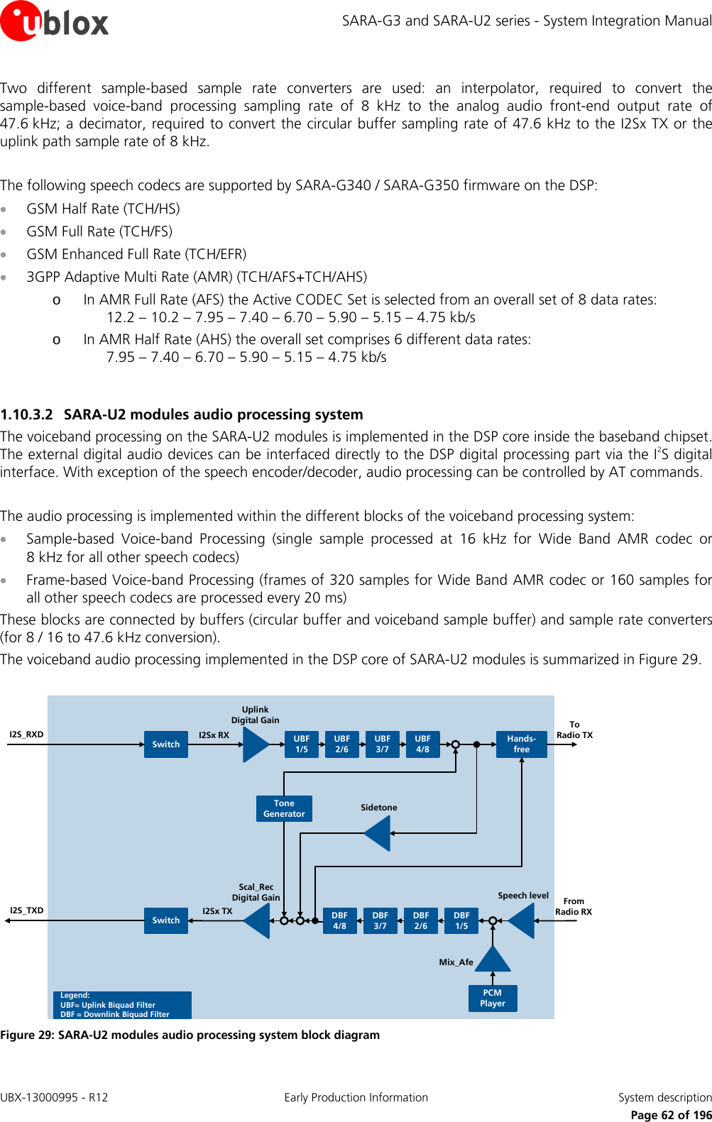
![SARA-G3 and SARA-U2 series - System Integration Manual SARA-U2 modules audio signal processing algorithms are: • Speech encoding (uplink) and decoding (downlink).The following speech codecs are supported in firmware on the DSP for speech encoding and decoding: GERAN GMSK codecs o GSM HR (GSM Half Rate) o GSM FR (GSM Full Rate) o GSM EFR (GSM Enhanced Full Rate) o HR AMR (GSM Half Rate Adaptive Multi Rate - Narrow Band) o FR AMR (GSM Full Rate Adaptive Multi Rate - Narrow Band) o FR AMR-WB (GSM Full Rate Adaptive Multi Rate - Wide Band) UTRAN codecs: o UMTS AMR2 (UMTS Adaptive Multi Rate version 2 – Narrow Band) o UMTS AMR-WB (UMTS Adaptive Multi Rate – Wide Band) • Mandatory sub-functions: o Discontinuous transmission, DTX (GSM 46.031, 46.041, 46.081 and 46.093 standards) o Voice activity detection, VAD (GSM 46.032, 46.042, 46.082 and 46.094 standards) o Background noise calculation (GSM 46.012, 46.022, 46.062 and 46.092 standards) • Function configurable via specific AT commands (refer to the u-blox AT Commands Manual [3]) o Signal routing: +USPM command o Analog amplification, digital amplification: +USGC, +CLVL, +CRSL, +CMUT command o Digital filtering: +UUBF, +UDBF commands o Hands-free algorithms (echo cancellation, Noise suppression, Automatic Gain control) +UHFP command o Sidetone generation (feedback of uplink speech signal to downlink path): +USTN command o Playing/mixing of alert tones: Service tones: Tone generator with 3 sinus tones +UPAR command User generated tones: Tone generator with a single sinus tone +UTGN command PCM audio files (for prompting): The storage format of PCM audio files is 8 kHz sample rate, signed 16 bits, little endian, mono UBX-13000995 - R12 Early Production Information System description Page 63 of 196](https://usermanual.wiki/u-blox/SARAU280/User-Guide-2520608-Page-63.png)
![SARA-G3 and SARA-U2 series - System Integration Manual 1.11 General Purpose Input/Output (GPIO) SARA-G300 and SARA-G310 modules do not support GPIOs. SARA-G340, SARA-G350 and SARA-U2 modules provide pins which can be configured as general purpose input or output, or can be configured to provide special functions via u-blox AT commands (for further details refer to the u-blox AT Commands Manual [3], +UGPIOC, +UGPIOR, +UGPIOW, +UGPS, +UGPRF): • SARA-G340 and SARA-G350 modules provide 4 configurable GPIO pins: GPIO1, GPIO2, GPIO3, GPIO4 • SARA-U2 modules provide 9 configurable GPIO pins: GPIO1, GPIO2, GPIO3, GPIO4, I2S_RXD, I2S_TXD, I2S_CLK, I2S_WA, SIM_DET The following functions are available: • Network status indication: The GPIO1, or the GPIO2, GPIO3, GPIO4 and, on SARA-U2 series only, the SIM_DET, alternatively from their default settings, can be configured to indicate network status (i.e. no service, registered home network, registered visitor network, voice or data call enabled), setting the parameter <gpio_mode> of AT+UGPIOC command to 2. No GPIO pin is by default configured to provide the “Network status indication” function. The “Network status indication” mode can be provided only on one pin per time: it is not possible to simultaneously set the same mode on another pin. The pin configured to provide the “Network status indication” function is set as o Continuous Low, if no service (no network coverage or not registered) o Cyclically High for 100 ms, Low for 2 s, if registered home 2G network o Cyclically High for 50 ms, Low for 50 ms, High for 50 ms, Low for 2 s, if registered home 3G network o Cyclically High for 100 ms, Low for 100 ms, High for 100 ms, Low for 2 s, if registered visitor 2G network (roaming) o Cyclically High for 50 ms, Low for 50 ms, High for 50 ms, Low for 100 ms, if registered visitor 3G network (roaming) o Continuous High, if voice or data 2G/3G call enabled • GSM Tx burst indication: GPIO1 pin can be configured by AT+UGPIOC to indicate when a GSM Tx burst/slot occurs, setting the parameter <gpio_mode> of AT+UGPIOC command to 9. No GPIO pin is by default configured to provide the “GSM Tx burst indication” function. The pin configured to provide the “GSM Tx burst indication” function is set as o High, since ~10 µs before the start of first Tx slot, until ~5 µs after the end of last Tx slot o Low, otherwise SARA-U280 module does not support the “GSM Tx burst indication” function on GPIO1, as the module does not support 2G radio access technology. UBX-13000995 - R12 Early Production Information System description Page 64 of 196](https://usermanual.wiki/u-blox/SARAU280/User-Guide-2520608-Page-64.png)
![SARA-G3 and SARA-U2 series - System Integration Manual • GNSS supply enable: The GPIO2 is by default configured by AT+UGPIOC command to enable or disable the supply of the u-blox GNSS receiver connected to the cellular module. The GPIO1, GPIO3, GPIO4 pins and, on SARA-U2 series only, also the SIM_DET pin, can be configured to provide the “GNSS supply enable” function, alternatively to the default GPIO2 pin, setting the parameter <gpio_mode> of AT+UGPIOC command to 3. The “GNSS supply enable” mode can be provided only on one pin per time: it is not possible to simultaneously set the same mode on another pin. The pin configured to provide the “GNSS supply enable” function is set as o High, to switch on the u-blox GNSS receiver, if AT+UGPS parameter <mode> is set to 1 o Low, to switch off the u-blox GNSS receiver, if AT+UGPS parameter <mode> is set to 0 (default) • GNSS data ready: Only the GPIO3 pin provides the “GNSS data ready” function, to sense when a u-blox GNSS receiver connected to the cellular module is ready to send data via the DDC (I2C) interface, setting the parameter <gpio_mode> of AT+UGPIOC command to 4. The pin configured to provide the “GNSS data ready” function is set as o Input, to sense the line status, waking up the cellular module from idle-mode when the u-blox GNSS receiver is ready to send data via the DDC (I2C) interface, if the first AT+UGPS parameter is set to 1 and the first AT+UGPRF parameter is set to 16 o Tri-state with an internal active pull-down enabled, otherwise (default setting) • GNSS RTC sharing: Only the GPIO4 pin provides the “GNSS RTC sharing” function, to provide an RTC (Real Time Clock) synchronization signal to the u-blox GNSS receiver connected to the cellular module, setting the parameter <gpio_mode> of AT+UGPIOC command to 5. The pin configured to provide the “GNSS RTC sharing” function is set as o Output, to provide an RTC (Real Time Clock) synchronization signal to the u-blox GNSS receiver if the first AT+UGPS parameter is set to 1 and the first AT+UGPRF parameter is set to 32 o Low, otherwise (default setting) • SIM card detection: The SIM_DET pin of SARA-G3 modules is by default configured to detect SIM card mechanical presence and this configuration cannot be changed by AT command. The SIM_DET pin of SARA-U2 modules is by default configured to detect SIM card mechanical presence as default setting of the AT+UGPIOC command: the “SIM card detection” function is enabled as the parameter <gpio_mode> of AT+UGPIOC command is set to 7 (default setting). The SIM_DET pin configured to provide the “SIM card detection” function is set as o Input with an internal active pull-down enabled, to sense SIM card mechanical presence The SIM_DET pin can sense the SIM card mechanical presence only if properly connected to the mechanical switch of a SIM card holder as described in section 2.5: o Low logic level at SIM_DET input pin is recognized as SIM card not present o High logic level at SIM_DET input pin is recognized as SIM card present SARA-U2 modules provide the additional function “SIM card hot insertion/removal” on the SIM_DET pin, which can be enabled using the AT+UDCONF=50 command if the “SIM card detection” function is enabled by AT+UGPIOC (for more details see u-blox AT Commands Manual [3]): in this case the SIM interface of the SARA-U2 modules is disabled when a Low logic level is recognized at SIM_DET input pin (within 20 ms from the start of the Low level) and it is enabled when an High logic level at SIM_DET input pin is recognized. SARA-G3 series do not support the additional function “SIM card hot insertion/removal” UBX-13000995 - R12 Early Production Information System description Page 65 of 196](https://usermanual.wiki/u-blox/SARAU280/User-Guide-2520608-Page-65.png)
![SARA-G3 and SARA-U2 series - System Integration Manual • Module status indication: The GPIO1 pin of SARA-U2 modules can be configured to indicate module status (power-off mode, i.e. module switched off, versus idle, active or connected mode, i.e. module switched on), by properly setting the parameter <gpio_mode> of AT+UGPIOC command to 10. No GPIO pin is by default configured to provide the “Module status indication”. The pin configured to provide the “Module status indication” function is set as o High, when the module is switched on (any operating mode during module normal operation) o Low, when the module is switched off (power off mode) SARA-G3 series do not support “Module status indication” function. • Module operating mode indication: The SIM_DET pin of SARA-U2 modules can be configured to indicate module operating mode status (the low power idle-mode versus active or connected mode), by properly setting the parameter <gpio_mode> of AT+UGPIOC command to 11. No GPIO pin is by default configured to provide the “Module operating mode indication”. The pin configured to provide the “Module operating mode indication” function is set as o Output / High, when the module is in active or connected mode o Output / Low, when the module is in idle-mode (that can be reached if power saving is enabled by +UPSV AT command: for further details see u-blox AT Commands Manual [3]) SARA-G3 series do not support “Module operating mode indication”. • I2S digital audio interface: The I2S_RXD, I2S_TXD, I2S_CLK, I2S_WA pins of SARA-U2 modules are by default configured as the I2S digital audio interface. Only these pins of SARA-U2 modules can be configured as the I2S digital audio interface, by correctly setting the parameter <gpio_mode> of AT+UGPIOC command to 12 (default setting). SARA-G3 series do not support the I2S digital audio interface over GPIOs. • General purpose input: All the GPIOs can be configured as input to sense high or low digital level through AT+UGPIOR command, setting the parameter <gpio_mode> of AT+UGPIOC command to 1. The “General purpose input” mode can be provided on more than one pin at a time. No GPIO pin is by default configured as “General purpose input”. The pin configured to provide the “General purpose input” function is set as o Input, to sense high or low digital level by AT+UGPIOR command. • General purpose output: All the GPIOs can be configured as output to set the high or the low digital level through AT+UGPIOW command, setting the parameter <gpio_mode> of +UGPIOC AT command to 0. The “General purpose output” mode can be provided on more than one pin per time. No GPIO pin is by default configured as “General purpose output”. The pin configured to provide the “General purpose output” function is set as o Output / Low, if the parameter <gpio_out_val> of AT+UGPIOW command is set to 0 o Output / High, if the parameter <gpio_out_val> of AT+UGPIOW command is set to 1 UBX-13000995 - R12 Early Production Information System description Page 66 of 196](https://usermanual.wiki/u-blox/SARAU280/User-Guide-2520608-Page-66.png)
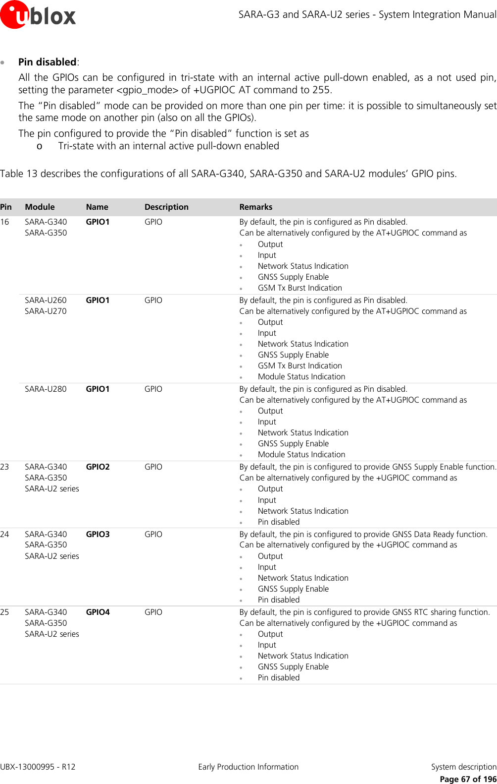
![SARA-G3 and SARA-U2 series - System Integration Manual 1.13 System features 1.13.1 Network indication Not supported by SARA-G300 and SARA-G310 modules. The GPIO1, or the GPIO2, GPIO3, GPIO4 and, on SARA-U2 series only, the SIM_DET, alternatively from their default settings, can be configured to indicate network status (i.e. no service, registered home network, registered visitor network, voice or data call enabled), by means of the AT+UGPIOC command. For the detailed description, see section 1.11 and to u-blox AT Commands Manual [3], GPIO commands. 1.13.2 Antenna detection Not supported by SARA-G300 and SARA-G310 modules. ANT_DET pin of SARA-G340, SARA-G350 and SARA-U2 series modules is an Analog to Digital Converter (ADC) provided to sense the presence of an external antenna when optionally set by the +UANTR AT command. The external antenna assembly must be provided with a built-in resistor (diagnostic circuit) to be detected, and an antenna detection circuit must be implemented on the application board properly connecting the antenna detection input (ANT_DET) to the antenna RF interface (ANT). For more details regarding feature description and detection / diagnostic circuit design-in see sections 1.7.2 and 2.4.2, and to the u-blox AT Commands Manual [3]. 1.13.3 Jamming detection Not supported by SARA-G300 and SARA-G310 modules. In real network situations modules can experience various kind of out-of-coverage conditions: limited service conditions when roaming to networks not supporting the specific SIM, limited service in cells which are not suitable or barred due to operators’ choices, no cell condition when moving to poorly served or highly interfered areas. In the latter case, interference can be artificially injected in the environment by a noise generator covering a given spectrum, thus obscuring the operator’s carriers entitled to give access to the cellular service. The Jamming Detection Feature detects such “artificial” interference and reports the start and stop of such conditions to the client, which can react appropriately by e.g. switching off the radio transceiver to reduce power consumption and monitoring the environment at constant periods. The feature detects, at radio resource level, an anomalous source of interference and signals it to the client with an unsolicited indication when the detection is entered or released. The jamming condition occurs when: • The module has lost synchronization with the serving cell and cannot select any other cell • The band scan reveals at least n carriers with power level equal or higher than threshold • On all such carriers, no synchronization is possible The client can configure the number of minimum disturbing carriers and the power level threshold by using the AT+UCD command [3]. The jamming condition is cleared when any of the above mentioned statements does not hold. The congestion (i.e. jamming) detection feature can be enabled and configured by the +UCD AT command (for more details see the u-blox AT Commands Manual [3]). UBX-13000995 - R12 Early Production Information System description Page 69 of 196](https://usermanual.wiki/u-blox/SARAU280/User-Guide-2520608-Page-69.png)
![SARA-G3 and SARA-U2 series - System Integration Manual 1.13.4 TCP/IP and UDP/IP Not supported by SARA-G300 and SARA-G310 modules. Via the AT commands it is possible to access the embedded TCP/IP and UDP/IP stack functionalities over the Packet Switched data connection. For more details about AT commands see u-blox AT Commands Manual [3]. Direct Link mode for TCP and UDP sockets is supported. Sockets can be set in Direct Link mode to establish a transparent end-to-end communication with an already connected TCP or UDP socket via serial interface. In Direct Link mode, data sent to the serial interface from an external application processor is forwarded to the network and vice-versa. To avoid data loss while using Direct Link, enable HW flow control on the serial interface. 1.13.5 FTP Not supported by SARA-G300 and SARA-G310 modules. SARA-G340, SARA-G350 and SARA-U2 series modules support the File Transfer Protocol functionalities via AT commands. Files are read and stored in the local file system of the module. SARA-U2 series modules support also Secure File Transfer Protocol functionalities providing SSL encryption. For more details about AT commands see the u-blox AT Commands Manual [3]. 1.13.6 HTTP Not supported by SARA-G300 and SARA-G310 modules. SARA-G340, SARA-G350 and SARA-U2 modules support Hyper-Text Transfer Protocol functionalities as an HTTP client is implemented: HEAD, GET, POST, DELETE and PUT operations are available. The file size to be uploaded / downloaded depends on the free space available in the local file system (FFS) at the moment of the operation. Up to 4 HTTP client contexts can simultaneously be used. SARA-U2 modules support also Secure Hyper-Text Transfer Protocol functionalities providing SSL encryption. For more details about AT commands see the u-blox AT Commands Manual [3]. 1.13.7 SMTP Not supported by SARA-G300, SARA-G310 and SARA-U2 modules. SARA-G340 and SARA-G350 modules support SMTP client functionalities. It is possible to specify the common parameters (e.g. server data, authentication method, etc. can be specified), to send an email to a SMTP server. Emails can be sent with or without attachment. Attachments are stored in the module local file system. For more details about AT commands see the u-blox AT Commands Manual [3]. UBX-13000995 - R12 Early Production Information System description Page 70 of 196](https://usermanual.wiki/u-blox/SARAU280/User-Guide-2520608-Page-70.png)
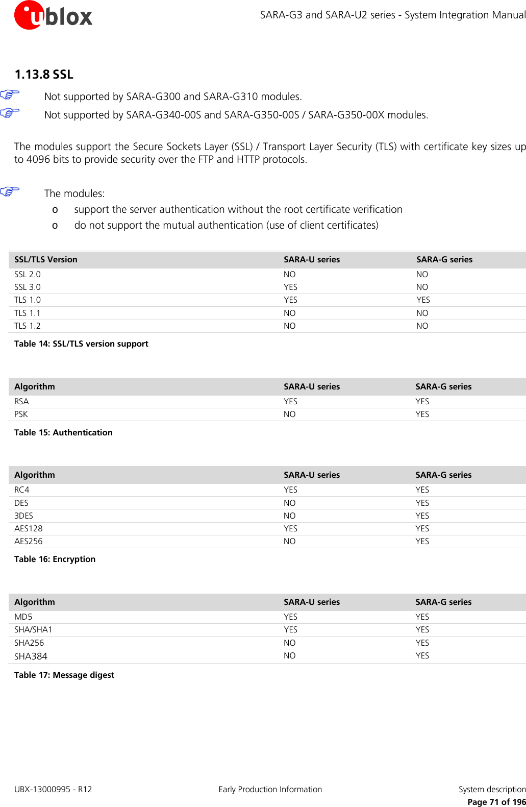
![SARA-G3 and SARA-U2 series - System Integration Manual Description Registry value SARA-U series SARA-G series TLS_RSA_WITH_AES_128_CBC_SHA 0x00,0x2F YES YES TLS_RSA_WITH_AES_128_CBC_SHA256 0x00,0x3C NO YES TLS_RSA_WITH_AES_256_CBC_SHA 0x00,0x35 NO YES TLS_RSA_WITH_AES_256_CBC_SHA256 0x00,0x3D NO YES TLS_RSA_WITH_3DES_EDE_CBC_SHA 0x00,0x0A NO YES TLS_RSA_WITH_DES_CBC_SHA 0x00,0x09 NO YES TLS_RSA_WITH_RC4_128_MD5 0x00,0x04 YES YES TLS_RSA_WITH_RC4_128_SHA 0x00,0x05 YES YES TLS_PSK_WITH_AES_128_CBC_SHA 0x00,0x8C NO YES TLS_PSK_WITH_AES_256_CBC_SHA 0x00,0x8D NO YES TLS_PSK_WITH_3DES_EDE_CBC_SHA 0x00,0x8B NO YES TLS_RSA_PSK_WITH_AES_128_CBC_SHA 0x00,0x94 NO YES TLS_RSA_PSK_WITH_AES_256_CBC_SHA 0x00,0x95 NO YES TLS_RSA_PSK_WITH_3DES_EDE_CBC_SHA 0x00,0x93 NO YES TLS_PSK_WITH_AES_128_CBC_SHA256 0x00,0xAE NO YES TLS_PSK_WITH_AES_256_CBC_SHA384 0x00,0xAF NO YES TLS_RSA_PSK_WITH_AES_128_CBC_SHA256 0x00,0xB6 NO YES TLS_RSA_PSK_WITH_AES_256_CBC_SHA384 0x00,0xB7 NO YES Table 18: TLS cipher suite registry 1.13.9 Dual stack IPv4/IPv6 Not supported by SARA-G3 modules. SARA-U2 modules support both Internet Protocol version 4 and Internet Protocol version 6. For more details about dual stack IPv4/IPv6 see the u-blox AT Commands Manual [3]. UBX-13000995 - R12 Early Production Information System description Page 72 of 196](https://usermanual.wiki/u-blox/SARAU280/User-Guide-2520608-Page-72.png)
![SARA-G3 and SARA-U2 series - System Integration Manual 1.13.10 Smart temperature management Not supported by SARA-G300 and SARA-G310 modules. Cellular modules – independent of the specific model – always have a well-defined operating temperature range. This range should be respected to guarantee full device functionality and long life span. Nevertheless there are environmental conditions that can affect operating temperature, e.g. if the device is located near a heating/cooling source, if there is/is not air circulating, etc. The module itself can also influence the environmental conditions; such as when it is transmitting at full power. In this case its temperature increases very quickly and can raise the temperature nearby. The best solution is always to properly design the system where the module is integrated. Nevertheless an extra check/security mechanism embedded into the module is a good solution to prevent operation of the device outside of the specified range. Smart Temperature Supervisor (STS) The Smart Temperature Supervisor is activated and configured by a dedicated AT+USTS command. See u-blox AT Commands Manual [3] for more details. The cellular module measures the internal temperature (Ti) and its value is compared with predefined thresholds to identify the actual working temperature range. Temperature measurement is done inside the module: the measured value could be different from the environmental temperature (Ta). Warningareat-1 t+1 t+2t-2Valid temperature rangeSafeareaDangerousarea Dangerousarea Warningarea Figure 30: Temperature range and limits The entire temperature range is divided into sub-regions by limits (see Figure 30) named t-2, t-1, t+1 and t+2. • Within the first limit, (t-1 < Ti < t+1), the cellular module is in the normal working range, the Safe Area • In the Warning Area, (t-2 < Ti < t.1) or (t+1 < Ti < t+2), the cellular module is still inside the valid temperature range, but the measured temperature approaches the limit (upper or lower). The module sends a warning to the user (through the active AT communication interface), which can take, if possible, the necessary actions to return to a safer temperature range or simply ignore the indication. The module is still in a valid and good working condition • Outside the valid temperature range, (Ti < t-2) or (Ti > t+2), the device is working outside the specified range and represents a dangerous working condition. This condition is indicated and the device shuts down to avoid damage For security reasons the shutdown is suspended in case an emergency call in progress. In this case the device switches off at call termination. The user can decide at anytime to enable/disable the Smart Temperature Supervisor feature. If the feature is disabled there is no embedded protection against disallowed temperature conditions. UBX-13000995 - R12 Early Production Information System description Page 73 of 196](https://usermanual.wiki/u-blox/SARAU280/User-Guide-2520608-Page-73.png)
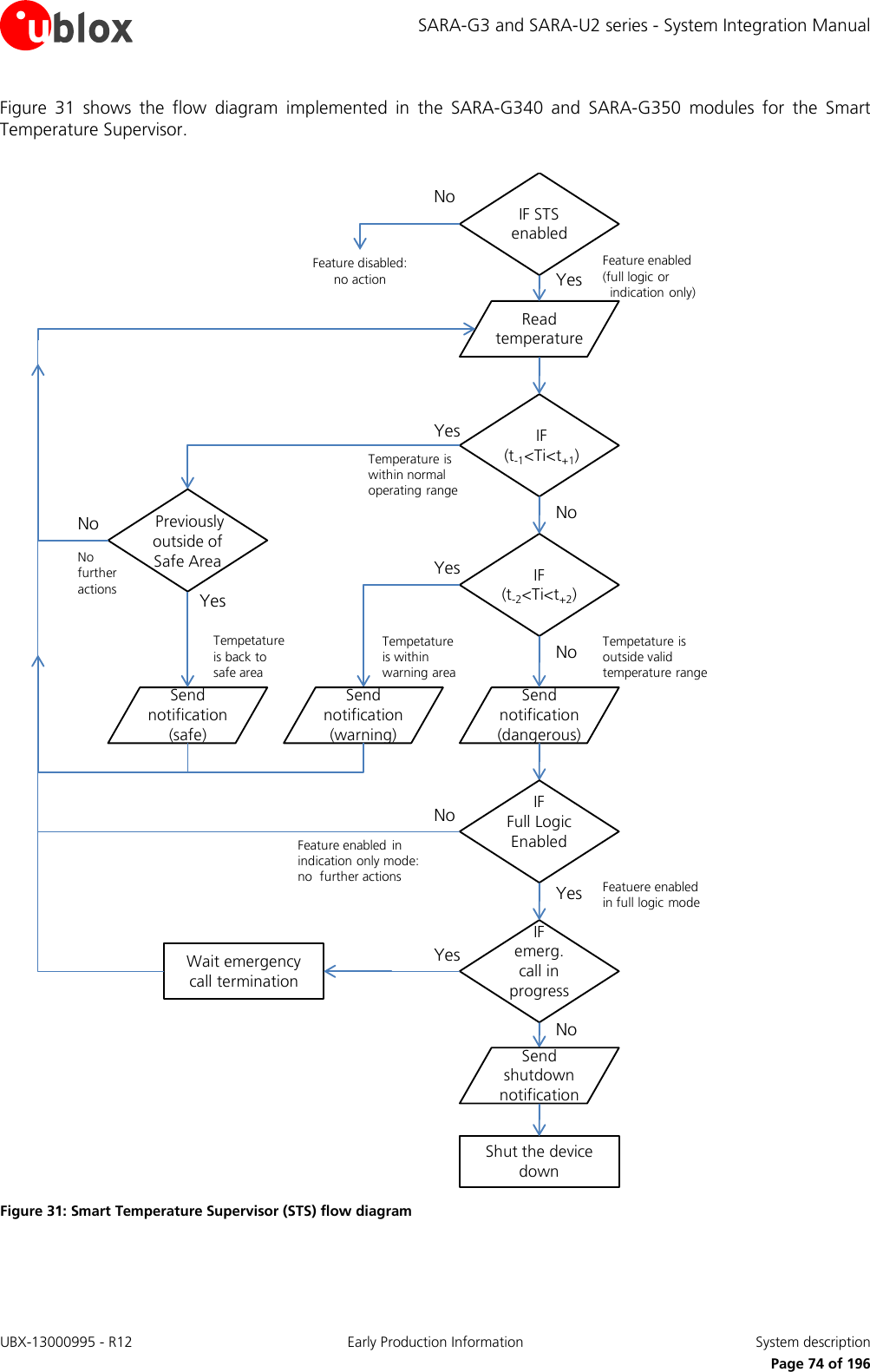
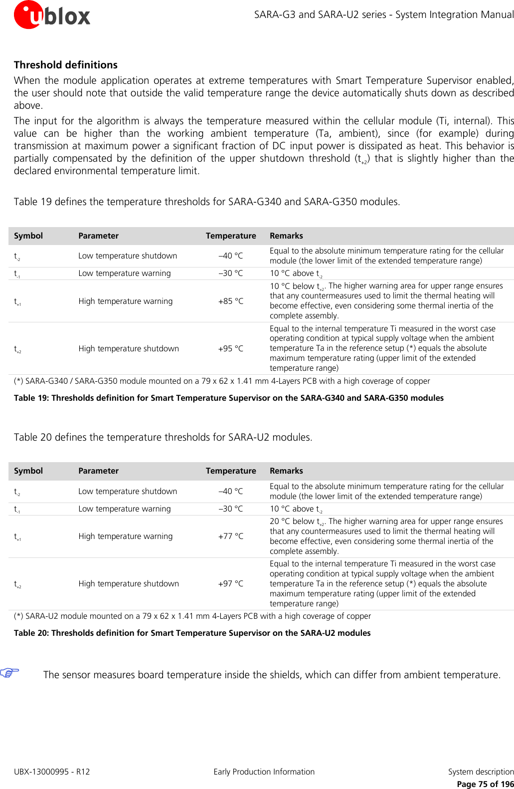
![SARA-G3 and SARA-U2 series - System Integration Manual 1.13.11 AssistNow clients and GNSS integration Not supported by SARA-G300 and SARA-G310 modules. For customers using u-blox GNSS receivers, SARA-G340, SARA-G350 and SARA-U2 modules feature embedded AssistNow clients. AssistNow A-GPS provides better GNSS performance and faster Time-To-First-Fix. The clients can be enabled and disabled with an AT command (see the u-blox AT Commands Manual [3]). SARA-G340, SARA-G350 and SARA-U2 modules act as a stand-alone AssistNow client, making AssistNow available with no additional requirements for resources or software integration on an external host micro controller. Full access to u-blox positioning receivers is available via the cellular modules, through a dedicated DDC (I2C) interface, while the available GPIOs can handle the positioning chipset / module power-on/off. This means that the cellular module and the positioning chips and modules can be controlled through a single serial port from any host processor. 1.13.12 Hybrid positioning and CellLocate® Not supported by SARA-G300 and SARA-G310 versions. Although GNSS is a widespread technology, reliance on the visibility of extremely weak GNSS satellite signals means that positioning is not always possible, particularly in shielded environments such as indoors and enclosed park houses, or when a GNSS jamming signal is present. The situation can be improved by augmenting GNSS receiver data with network cell information to provide a level of redundancy that can benefit numerous applications. Positioning through cellular information: CellLocate® u-blox CellLocate® enables the device position estimation based on the parameters of the mobile network cells visible to the specific device. To estimate its position the module sends the CellLocate® server the parameters of network cells visible to it using a UDP connection. In return the server provides the estimated position based on the CellLocate® database. SARA-G340, SARA-G350 and SARA-U2 modules can either send the parameters of the visible home network cells only (normal scan) or the parameters of all surrounding cells of all mobile operators (deep scan). The CellLocate® database is compiled from the position of devices which observed, in the past, a specific cell or set of cells (historical observations) as follows: UBX-13000995 - R12 Early Production Information System description Page 76 of 196](https://usermanual.wiki/u-blox/SARAU280/User-Guide-2520608-Page-76.png)
![SARA-G3 and SARA-U2 series - System Integration Manual 4. The visibility of multiple cells provides increased accuracy based on the intersection of areas of visibility. CellLocate® is implemented using a set of two AT commands that allow configuration of the CellLocate® service (AT+ULOCCELL) and requesting position according to the user configuration (AT+ULOC). The answer is provided in the form of an unsolicited AT command including latitude, longitude and estimated accuracy. The accuracy of the position estimated by CellLocate® depends on the availability of historical observations in the specific area. Hybrid positioning With u-blox hybrid positioning technology, u-blox cellular modules can be triggered to provide their current position using either a u-blox GNSS receiver or the position estimated from CellLocate®. The choice depends on which positioning method provides the best and fastest solution according to the user configuration, exploiting the benefit of having multiple and complementary positioning methods. Hybrid positioning is implemented through a set of three AT commands that allow GNSS receiver configuration (AT+ULOCGNSS), CellLocate® service configuration (AT+ULOCCELL), and requesting the position according to the user configuration (AT+ULOC). The answer is provided in the form of an unsolicited AT command including latitude, longitude and estimated accuracy (if the position has been estimated by CellLocate®), and additional parameters if the position has been computed by the GNSS receiver. The configuration of mobile network cells does not remain static (e.g. new cells are continuously added or existing cells are reconfigured by the network operators). For this reason, when a hybrid positioning method has been triggered and the GNSS receiver calculates the position, a database self-learning mechanism has been implemented so that these positions are sent to the server to update the database and maintain its accuracy. The use of hybrid positioning requires a connection via the DDC (I2C) bus between the cellular modules and the u-blox GNSS receiver (see section 2.6.4). See GNSS Implementation Application Note [24] for the complete description of the feature. u-blox is extremely mindful of user privacy. When a position is sent to the CellLocate® server u-blox is unable to track the SIM used or the specific device. UBX-13000995 - R12 Early Production Information System description Page 78 of 196](https://usermanual.wiki/u-blox/SARAU280/User-Guide-2520608-Page-78.png)
![SARA-G3 and SARA-U2 series - System Integration Manual 1.13.13 Firmware upgrade Over AT (FOAT) Overview This feature allows upgrading the module Firmware over the AT interface of the module (the UART for SARA-G3 modules, the UART or the USB for SARA-U2 modules), using AT Commands. • The AT+UFWUPD command triggers a reboot followed by the upgrade procedure at specified a baud rate (see u-blox AT Commands Manual [3] for more details) • A special boot loader on the module performs firmware installation, security verifications and module reboot • Firmware authenticity verification is performed via a security signature during the download. The firmware is then installed, overwriting the current version. In case of power loss during this phase, the boot loader detects a fault at the next wake-up, and restarts the firmware download from the Xmodem-1k handshake. After completing the upgrade, the module is reset again and wakes-up in normal boot FOAT procedure The application processor must proceed in the following way: • Send the AT+UFWUPD command through the AT interface, specifying file type and desired baud rate • Reconfigure serial communication at selected baud rate, with the used protocol • Send the new FW image via the used protocol For more details, see the Firmware Update Application Note [25]. 1.13.14 Firmware upgrade Over The Air (FOTA) Not supported by SARA-G300 and SARA-G310 modules and SARA-U2 series. Supported upon request on SARA-G340 and SARA-G350 modules. This feature allows upgrading the module firmware over the air, i.e. over the cellular network. The main idea with updating firmware over the air is to reduce the amount of data required for transmission to the module. This is achieved by downloading only a “delta file” instead of the full firmware. The delta contains only the differences between the two firmware versions (old and new), and is compressed. For more details, see the Firmware Update Application Note [25]. UBX-13000995 - R12 Early Production Information System description Page 79 of 196](https://usermanual.wiki/u-blox/SARAU280/User-Guide-2520608-Page-79.png)
![SARA-G3 and SARA-U2 series - System Integration Manual 1.13.15 In-Band modem (eCall / ERA-GLONASS) Not supported by SARA-G300 / SARA-G310 / SARA-U260 / SARA-U280 modules. SARA-G340, SARA-G350 and SARA-U2 modules support an In-Band modem solution for the European eCall and the Russian ERA-GLONASS emergency call applications over cellular networks, implemented according to 3GPP TS 26.267 [22], BS EN 16062:2011 [30] and ETSI TS 122 101 [31] specifications. eCall (European) and ERA-GLONASS (Russian) are initiatives to combine mobile communications and satellite positioning to provide rapid assistance to motorists in the event of a collision. The eCall automated emergency response system is based on GPS, and the ERA-GLONASS is based on the GLONASS positioning system. When activated, the in-vehicle systems (IVS) automatically initiate an emergency call carrying both voice and data (including location data) directly to the nearest Public Safety Answering Point (PSAP) to determine whether rescue services should be dispatched to the known position. Figure 32: eCall and ERA-GLONASS automated emergency response systems diagram flow For more details regarding the In-Band modem solution for the European eCall and the Russian ERA-GLONASS emergency call applications see the u-blox eCall / ERA-GLONASS Application Note [29]. 1.13.16 SIM Access Profile (SAP) Not supported by SARA-G3 modules. SIM access profile (SAP) feature allows SARA-U2 modules to access and use a remote (U)SIM card instead of the local SIM card directly connected to the module (U)SIM interface. SARA-U2 modules provide a dedicated USB SAP channel and dedicated multiplexer SAP channel over UART for communication with the remote (U)SIM card. The communication between SARA-U2 modules and the remote SIM is conformed to client-server paradigm: the SARA-U2 module is the SAP client establishing a connection and performing data exchange to an SAP server directly connected to the remote SIM that is used by SARA-U2 module for GSM/UMTS network operations. The SAP communication protocol is based on the SIM Access Profile Interoperability Specification [28]. SARA-U2 modules do not support SAP server role: the module acts as SAP client only. A typical application using the SAP feature is the scenario where a device such as an embedded car-phone with an integrated SARA-U2 module uses a remote SIM included in an external user device (e.g. a simple SIM card reader or a portable phone), which is brought into the car. The car-phone accesses the GSM/UMTS network using the remote SIM in the external device. UBX-13000995 - R12 Early Production Information System description Page 80 of 196](https://usermanual.wiki/u-blox/SARAU280/User-Guide-2520608-Page-80.png)
![SARA-G3 and SARA-U2 series - System Integration Manual SARA-U2 modules, acting as an SAP client, can be connected to an SAP server by a completely wired connection, as shown in Figure 33. Device including SARA-U2 GSM/UMTS InterfaceSAP Serial Interface(SAP channel over USB or UART)Local SIM(optional)SARA-U2SAP ClientApplicationProcessorDevice including SIMSAP Serial InterfaceRemote SIMMobileEquipmentSAP Server Figure 33: Remote SIM access via completely wired connection As stated in the SIM Access Profile Interoperability Specification [28], the SAP client can be connected to the SAP server by means of a Bluetooth wireless link, using additional Bluetooth transceivers. In this case, the application processor wired to SARA-U2 modules establishes and controls the Bluetooth connection using the SAP profile, and routes data received over a serial interface channel to data transferred over a Bluetooth interface and vice versa, as shown in Figure 34. Device including SARA-U2SAP Serial Interface(SAP channel o ver USB or UART)GSM/UMTS InterfaceLocal SIM(optional)SARA-U2SAP ClientApplicationProcessorSAP Bluetooth InterfaceBluetoothTransceiverDevice including SIMRemote SIMMobileEquipmentSAP ServerBluetoothTransceiver Figure 34: Remote SIM access via Bluetooth and wired connection The application processor can start an SAP connection negotiation between SARA-U2 module SAP client and an SAP server using custom AT command (for more details refer to u-blox AT Commands Manual [3]). While the connection with the SAP server is not fully established, the SARA-U2 module continues to operate with the attached (local) SIM, if present. Once the connection is established and negotiated, the SARA-U2 module performs a detach operation from the local SIM followed by an attach operation to the remote one. Then the remotely attached SIM is used for any GSM/UMTS network operation. URC indications are provided to inform the user about the state of both the local and remote SIM. The insertion and the removal of the local SIM card are notified if a proper card presence detection circuit using the SIM_DET pin of SARA-U2 modules is implemented as shown in the section 2.5, and if the related “SIM card detection” and “SIM hot insertion/removal” functions are enabled by AT commands (for more details see u-blox AT Commands Manual [3], +UGPIOC, +UDCONF=50 AT commands). Upon SAP deactivation, the SARA-U2 modules perform a detach operation from the remote SIM followed by an attach operation to the local one, if present. UBX-13000995 - R12 Early Production Information System description Page 81 of 196](https://usermanual.wiki/u-blox/SARAU280/User-Guide-2520608-Page-81.png)
![SARA-G3 and SARA-U2 series - System Integration Manual 1.13.17 Power saving The power saving configuration is by default disabled, but it can be enabled using the AT+UPSV command. When power saving is enabled, the module automatically enters the low power idle-mode whenever possible, reducing current consumption. During low power idle-mode, the module is not ready to communicate with an external device by means of the application interfaces, since it is configured to reduce power consumption. It can be woken up from idle-mode to active-mode by the connected application processor, by the connected u-blox positioning receiver or by network activities, as described in Table 6. During idle-mode, the module processor core runs with the RTC 32 kHz reference clock, which is generated by: • The internal 32 kHz oscillator, in case of SARA-G340, SARA-G350 and SARA-U2 modules • The 32 kHz signal provided at the EXT32K input pin, in case of SARA-G300 and SARA-G310 modules SARA-G300 and SARA-G310 need a 32 kHz signal at EXT32K input to reach the low power idle-mode. For the complete description of the AT+UPSV command, refer to the u-blox AT Commands Manual [3]. For the definition and the description of SARA-G3 and SARA-U2 series modules operating modes, including the events forcing transitions between the different operating modes, refer to section 1.4. For the description of current consumption in idle and active operating modes, refer to sections 1.5.1.4, 1.5.1.5. For the description of the UART settings related to module power saving configuration, refer to section 1.9.1.4. For the description of the USB settings related to module power saving configuration, refer to section 1.9.3.2. For the description of the EXT32K input and related application circuit design-in, refer to sections 1.6.4, 2.3.3. UBX-13000995 - R12 Early Production Information System description Page 82 of 196](https://usermanual.wiki/u-blox/SARAU280/User-Guide-2520608-Page-82.png)
![SARA-G3 and SARA-U2 series - System Integration Manual voltage (e.g. ~12 V), whereas a linear charger is the typical choice when the charging source has a relatively low nominal voltage (~5 V). If both a permanent primary supply / charging source (e.g. ~12 V) and a rechargeable back-up battery (e.g. 3.7 V Li-Pol) are available at the same time in the application as possible supply source, then a proper charger / regulator with integrated power path management function can be selected to supply the module while simultaneously and independently charging the battery. Refer to sections 2.2.1.7, 2.2.1.8, 2.2.1.6, 2.2.1.9, and 2.2.1.10 for specific design-in. The use of a primary (not rechargeable) battery is in general uncommon, but appropriate parts can be selected given that the most cells available are seldom capable of delivering the burst peak current for a GSM call due to high internal resistance. Refer to sections 2.2.1.5, 2.2.1.6, 2.2.1.9, and 2.2.1.10 for specific design-in. The usage of more than one DC supply at the same time should be carefully evaluated: depending on the supply source characteristics, different DC supply systems can result as mutually exclusive. The usage of a regulator or a battery not able to support the highest peak of VCC current consumption specified in the SARA-G3 series Data Sheet [1] and in the SARA-U2 series Data Sheet [2] is generally not recommended. However, if the selected regulator or battery is not able to support the highest peak current of the module, it must be able to support at least the highest averaged current consumption value specified in the SARA-G3 series Data Sheet [1] and in the SARA-U2 series Data Sheet [2]. The additional energy required by the module during a 2G Tx slot can be provided by an appropriate bypass tank capacitor or supercapacitor with very large capacitance and very low ESR placed close to the module VCC pins. Depending on the actual capability of the selected regulator or battery, the required capacitance can be considerably larger than 1 mF and the required ESR can be in the range of few tens of mΩ. Carefully evaluate the implementation of this solution since aging and temperature conditions significantly affect the actual capacitor characteristics. The following sections highlight some design aspects for each of the supplies listed above providing application circuit design-in compliant with the module VCC requirements summarized in Table 7. For the additional specific guidelines for SARA-G350 ATEX and SARA-U270 ATEX modules integration in potentially explosive atmospheres applications, refer to section 2.14. 2.2.1.2 Guidelines for VCC supply circuit design using a switching regulator The use of a switching regulator is suggested when the difference from the available supply rail to the VCC value is high: switching regulators provide good efficiency transforming a 12 V or greater voltage supply to the typical 3.8 V value of the VCC supply. The characteristics of the switching regulator connected to VCC pins should meet the following prerequisites to comply with the module VCC requirements summarized in Table 7: • Power capability: the switching regulator with its output circuit must be capable of providing a voltage value to the VCC pins within the specified operating range and must be capable of delivering to VCC pins the specified maximum peak / pulse current with 1/8 duty cycle (refer to the SARA-G3 series Data Sheet [1] or the SARA-U2 series Data Sheet [2]). • Low output ripple: the switching regulator together with its output circuit must be capable of providing a clean (low noise) VCC voltage profile. • High switching frequency: for best performance and for smaller applications select a switching frequency ≥ 600 kHz (since L-C output filter is typically smaller for high switching frequency). The use of a switching regulator with a variable switching frequency or with a switching frequency lower than 600 kHz must be carefully evaluated since this can produce noise in the VCC voltage profile and therefore negatively impact GSM modulation spectrum performance. An additional L-C low-pass filter between the switching regulator output to VCC supply pins can mitigate the ripple on VCC, but adds extra voltage drop due to resistive losses on series inductors. UBX-13000995 - R12 Early Production Information Design-in Page 85 of 196](https://usermanual.wiki/u-blox/SARAU280/User-Guide-2520608-Page-85.png)
![SARA-G3 and SARA-U2 series - System Integration Manual Figure 37 and the components listed in Table 22 show an example of a low cost power supply circuit, where the VCC module supply is provided by a step-down switching regulator capable of delivering to VCC pins the specified maximum peak / pulse current, transforming a 12 V supply input. SARA-G3 / SARA-U212VR5C6C1VCCINHFSWSYNCOUTGND263178C3C2D1 R1R2L1U1GNDFBCOMP54R3C4R4C552 VCC53 VCC51 VCC Figure 37: Suggested low cost solution for the VCC voltage supply application circuit using step-down regulator Reference Description Part Number - Manufacturer C1 22 µF Capacitor Ceramic X5R 1210 10% 25 V GRM32ER61E226KE15 – Murata C2 100 µF Capacitor Tantalum B_SIZE 20% 6.3V 15mΩ T520B107M006ATE015 – Kemet C3 5.6 nF Capacitor Ceramic X7R 0402 10% 50 V GRM155R71H562KA88 – Murata C4 6.8 nF Capacitor Ceramic X7R 0402 10% 50 V GRM155R71H682KA88 – Murata C5 56 pF Capacitor Ceramic C0G 0402 5% 50 V GRM1555C1H560JA01 – Murata C6 220 nF Capacitor Ceramic X7R 0603 10% 25 V GRM188R71E224KA88 – Murata D1 Schottky Diode 25V 2 A STPS2L25 – STMicroelectronics L1 5.2 µH Inductor 30% 5.28A 22 mΩ MSS1038-522NL – Coilcraft R1 4.7 kΩ Resistor 0402 1% 0.063 W RC0402FR-074K7L – Yageo R2 910 Ω Resistor 0402 1% 0.063 W RC0402FR-07910RL – Yageo R3 82 Ω Resistor 0402 5% 0.063 W RC0402JR-0782RL – Yageo R4 8.2 kΩ Resistor 0402 5% 0.063 W RC0402JR-078K2L – Yageo R5 39 kΩ Resistor 0402 5% 0.063 W RC0402JR-0739KL – Yageo U1 Step-Down Regulator 8-VFQFPN 3 A 1 MHz L5987TR – ST Microelectronics Table 22: Suggested components for low cost solution VCC voltage supply application circuit using a step-down regulator 2.2.1.3 Guidelines for VCC supply circuit design using a Low Drop-Out (LDO) linear regulator The use of a linear regulator is suggested when the difference from the available supply rail and the VCC value is low: linear regulators provide high efficiency when transforming a 5 V supply to a voltage value within the module VCC normal operating range. The characteristics of the LDO linear regulator connected to the VCC pins should meet the following prerequisites to comply with the module VCC requirements summarized in Table 7: • Power capabilities: the LDO linear regulator with its output circuit must be capable of providing a proper voltage value to the VCC pins and of delivering to VCC pins the specified maximum peak / pulse current with 1/8 duty cycle (refer to the SARA-G3 series Data Sheet [1] or the SARA-U2 series Data Sheet [2]). • Power dissipation: the power handling capability of the LDO linear regulator must be checked to limit its junction temperature to the maximum rated operating range (i.e. check the voltage drop from the max input voltage to the min output voltage to evaluate the power dissipation of the regulator). UBX-13000995 - R12 Early Production Information Design-in Page 87 of 196](https://usermanual.wiki/u-blox/SARAU280/User-Guide-2520608-Page-87.png)
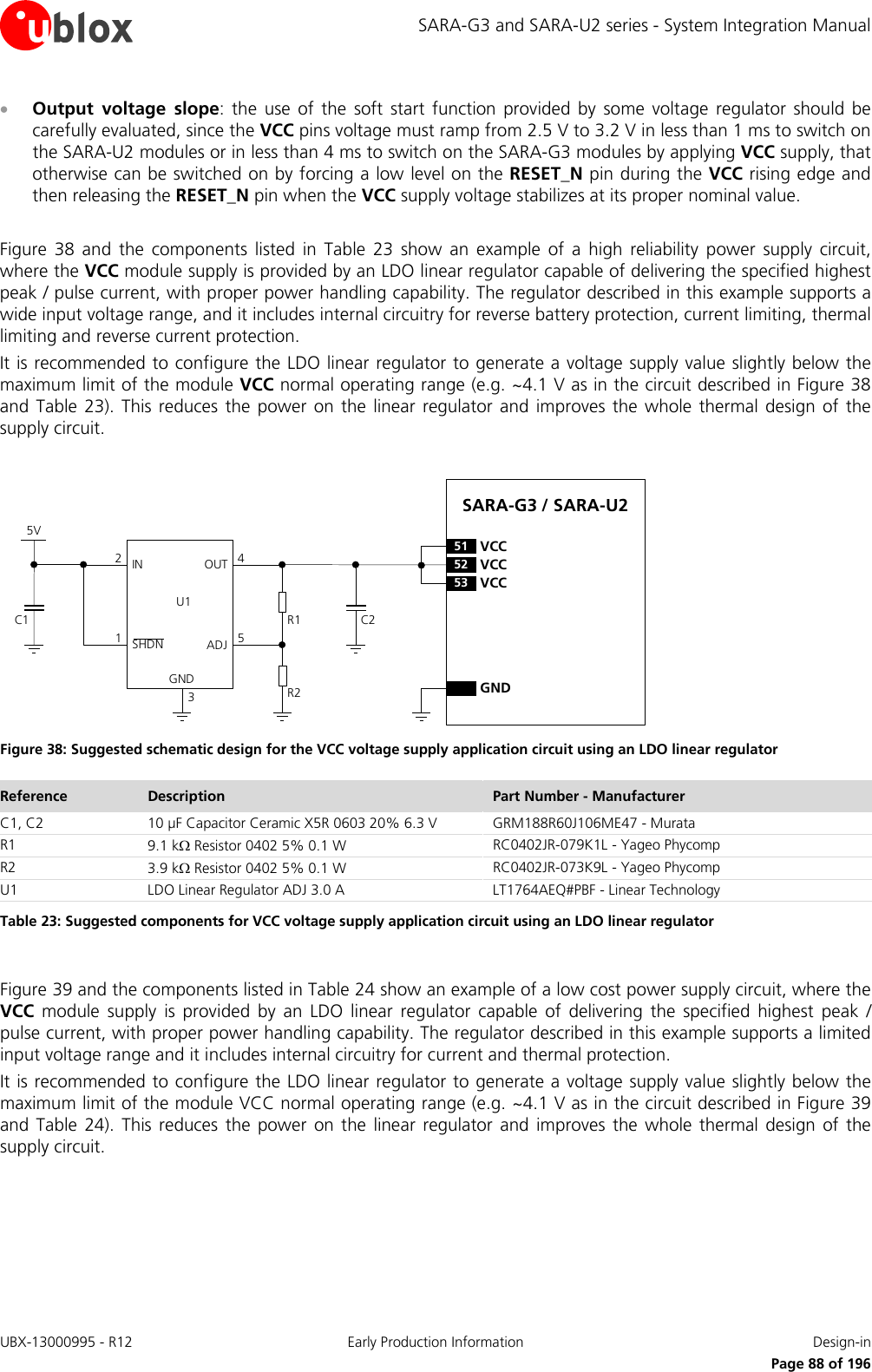
![SARA-G3 and SARA-U2 series - System Integration Manual 5VC1IN OUTADJGND12453C2R1R2U1ENSARA-G3 / SARA-U252VCC53VCC51VCCGND Figure 39: Suggested schematic design for the VCC voltage supply application circuit using an LDO linear regulator Reference Description Part Number - Manufacturer C1, C2 10 µF Capacitor Ceramic X5R 0603 20% 6.3 V GRM188R60J106ME47 - Murata R1 27 kΩ Resistor 0402 5% 0.1 W RC0402JR-0727KL - Yageo Phycomp R2 4.7 kΩ Resistor 0402 5% 0.1 W RC0402JR-074K7L - Yageo Phycomp U1 LDO Linear Regulator ADJ 3.0 A LP38501ATJ-ADJ/NOPB - Texas Instrument Table 24: Suggested components for VCC voltage supply application circuit using an LDO linear regulator 2.2.1.4 Guidelines for VCC supply circuit design using a rechargeable Li-Ion or Li-Pol battery Rechargeable Li-Ion or Li-Pol batteries connected to the VCC pins should meet the following prerequisites to comply with the module VCC requirements summarized in Table 7: • Maximum pulse and DC discharge current: the rechargeable Li-Ion battery with its output circuit must be capable of delivering to VCC pins the specified maximum peak / pulse current with 1/8 duty cycle, and a DC current greater than the module maximum average current consumption (refer to the SARA-G3 series Data Sheet [1] or the SARA-U2 series Data Sheet [2]). The maximum pulse discharge current and the maximum DC discharge current are not always reported in battery data sheets, but the maximum DC discharge current is typically almost equal to the battery capacity in Amp-hours divided by 1 hour. • DC series resistance: the rechargeable Li-Ion battery with its output circuit must be capable of avoiding a VCC voltage drop greater than 400 mV during transmit bursts. 2.2.1.5 Guidelines for VCC supply circuit design using a primary (disposable) battery The characteristics of a primary (non-rechargeable) battery connected to VCC pins should meet the following prerequisites to comply with the module VCC requirements summarized in Table 7: • Maximum pulse and DC discharge current: the non-rechargeable battery with its output circuit must be capable of delivering to VCC pins the specified maximum peak / pulse current with 1/8 duty cycle, and a DC current greater than the module maximum average current consumption (refer to the SARA-G3 series Data Sheet [1] or the SARA-U2 series Data Sheet [2]). The maximum pulse and the maximum DC discharge current is not always reported in battery data sheets, but the maximum DC discharge current is typically almost equal to the battery capacity in Amp-hours divided by 1 hour. • DC series resistance: the non-rechargeable battery with its output circuit must be capable of avoiding a VCC voltage drop greater than 400 mV during transmit bursts. UBX-13000995 - R12 Early Production Information Design-in Page 89 of 196](https://usermanual.wiki/u-blox/SARAU280/User-Guide-2520608-Page-89.png)
![SARA-G3 and SARA-U2 series - System Integration Manual 2.2.1.6 Additional guidelines for VCC supply circuit design To reduce voltage drops, use a low impedance power source. The resistance of the power supply lines (connected to the VCC and GND pins of the module) on the application board and battery pack should also be considered and minimized: cabling and routing must be as short as possible to minimize power losses. Three pins are allocated for VCC supply. Another twenty pins are designated for GND connection. Even if all the VCC pins and all the GND pins are internally connected within the module, it is recommended to properly connect all of them to supply the module to minimize series resistance losses. To avoid voltage drop undershoot and overshoot at the start and end of a transmit burst during a single-slot 2G voice/data call (when current consumption on the VCC supply can rise up to the maximum peak / pulse current specified in the SARA-G3 series Data Sheet [1] or in the SARA-U2 series Data Sheet [2]), place a bypass capacitor with large capacitance (more than 100 µF) and low ESR near the VCC pins, for example: • 330 µF capacitance, 45 mΩ ESR (e.g. KEMET T520D337M006ATE045, Tantalum Capacitor) The use of very large capacitors (i.e. greater then 1000 µF) on the VCC line should be carefully evaluated, since the voltage at the VCC pins voltage must ramp from 2.5 V to 3.2 V in less than 1 ms to switch on the SARA-U2 modules or in less than 4 ms to switch on the SARA-G3 modules by applying VCC supply, that otherwise can be switched on by forcing a low level on the RESET_N pin during the VCC rising edge and then releasing the RESET_N pin when the VCC supply voltage stabilizes at its proper nominal value. To reduce voltage ripple and noise, especially if the application device integrates an internal antenna, place the following bypass capacitors near the VCC pins: • 100 nF capacitor (e.g Murata GRM155R61C104K) to filter digital logic noise from clocks and data sources • 10 nF capacitor (e.g. Murata GRM155R71C103K) to filter digital logic noise from clocks and data sources • 56 pF capacitor with Self-Resonant Frequency in 800/900 MHz range (e.g. Murata GRM1555C1E560J) to filter transmission EMI in the GSM/EGSM bands • 15 pF capacitor with Self-Resonant Frequency in 1800/1900 MHz range (e.g. Murata GRM1555C1E150J) to filter transmission EMI in the DCS/PCS bands A series ferrite bead for GHz band noise (e.g. Murata BLM18EG221SN1) can be placed close to the VCC pins of the module for additional noise filtering, but in general it is not strictly required. Figure 40 shows the complete configuration but the mounting of each single component depends on the application design: it is recommended to provide all the VCC bypass capacitors as described in Figure 40 and Table 25 if the application device integrates an internal antenna. C4GNDC3 C2SARA-G3 / SARA-U252VCC53VCC51VCC3V8C1+C5 Figure 40: Suggested schematic and layout design for the VCC bypass capacitors to reduce ripple / noise on VCC voltage profile and to avoid undershoot / overshoot on VCC voltage drops UBX-13000995 - R12 Early Production Information Design-in Page 90 of 196](https://usermanual.wiki/u-blox/SARAU280/User-Guide-2520608-Page-90.png)
![SARA-G3 and SARA-U2 series - System Integration Manual 2.2.2 RTC supply (V_BCKP) 2.2.2.1 Guidelines for V_BCKP circuit design If RTC timing is required to run for a time interval of T [s] at 25 °C when VCC supply is removed, place a capacitor with a nominal capacitance of C [µF] at the V_BCKP pin. Choose the capacitor using the following formula: C [µF] = (Current_Consumption [µA] x T [s]) / Voltage_Drop [V] = 1.5 x T [s] for SARA-G3 series = 2.5 x T [s] for SARA-U2 series For example, a 100 µF capacitor (such as the Murata GRM43SR60J107M) can be placed at V_BCKP to provide a long buffering time. This capacitor holds V_BCKP voltage within its valid range for around 70 s (SARA-G3 series) or for around 40 s (SARA-U2 series) at 25 °C, after the VCC supply is removed. If a very long buffering time is required, a 70 mF super-capacitor (e.g. Seiko Instruments XH414H-IV01E) can be placed at V_BCKP, with a 4.7 kΩ series resistor to hold the V_BCKP voltage within its valid range for ~13 hours (SARA-G3 series) or for ~8 hours (SARA-U2 series) at 25 °C, after the VCC supply is removed. The purpose of the series resistor is to limit the capacitor charging current due to the large capacitor specifications, and also to let a fast rise time of the voltage value at the V_BCKP pin after VCC supply has been provided. These capacitors allow the time reference to run during battery disconnection. SARA-G3 seriesSARA-U2 seriesC1(a)2V_BCKPR2SARA-G3 seriesSARA-U2 seriesC2(superCap)(b)2V_BCKPD3SARA-G3 seriesSARA-U2 seriesB3(c)2V_BCKP Figure 44: Real time clock supply (V_BCKP) application circuits: (a) using a 100 µF capacitor to let the RTC run for ~1 minute after VCC removal; (b) using a 70 mF capacitor to let RTC run for ~10 hours after VCC removal; (c) using a non-rechargeable battery Reference Description Part Number - Manufacturer C1 100 µF Tantalum Capacitor GRM43SR60J107M - Murata R2 4.7 kΩ Resistor 0402 5% 0.1 W RC0402JR-074K7L - Yageo Phycomp C2 70 mF Capacitor XH414H-IV01E - Seiko Instruments Table 28: Example of components for V_BCKP buffering If longer buffering time is required to allow the RTC time reference to run during a disconnection of the VCC supply, then an external battery can be connected to V_BCKP pin. The battery should be able to provide a proper nominal voltage and must never exceed the maximum operating voltage for V_BCKP (specified in the Input characteristics of Supply/Power pins table in the SARA-G3 series Data Sheet [1] or in the SARA-U2 series Data Sheet [2]). The connection of the battery to V_BCKP should be done with a suitable series resistor for a rechargeable battery, or with an appropriate series diode for a non-rechargeable battery. The purpose of the series resistor is to limit the battery charging current due to the battery specifications, and also to allow a fast rise time of the voltage value at the V_BCKP pin after the VCC supply has been provided. The purpose of the series diode is to avoid a current flow from the module V_BCKP pin to the non-rechargeable battery. If the RTC timing is not required when the VCC supply is removed, it is not needed to connect the V_BCKP pin to an external capacitor or battery. In this case the date and time are not updated when VCC UBX-13000995 - R12 Early Production Information Design-in Page 96 of 196](https://usermanual.wiki/u-blox/SARAU280/User-Guide-2520608-Page-96.png)
![SARA-G3 and SARA-U2 series - System Integration Manual is disconnected. If VCC is always supplied, then the internal regulator is supplied from the main supply and there is no need for an external component on V_BCKP. Combining a SARA-G3 or a SARA-U2 cellular module with a u-blox GNSS positioning receiver, the positioning receiver VCC supply is controlled by the cellular module by means of the “GNSS supply enable” function provided by the GPIO2 of the cellular module. In this case the V_BCKP supply output of the cellular module can be connected to the V_BCKP backup supply input pin of the GNSS receiver to provide the supply for the positioning real time clock and backup RAM when the VCC supply of the cellular module is within its operating range and the VCC supply of the GNSS receiver is disabled. This enables the u-blox GNSS receiver to recover from a power breakdown with either a hot start or a warm start (depending on the duration of the positioning VCC outage) and to maintain the configuration settings saved in the backup RAM. Refer to section 2.6.4 for more details regarding the application circuit with a u-blox GNSS receiver. On SARA-G300 and SARA-G310 modules, the V_BCKP supply output can be used to supply an external 32 kHz oscillator which provides a 32 kHz signal to the EXT32K input pin as reference clock for the RTC timing, so that the modules can enter the low power idle-mode and can make available the RTC functions. The internal regulator for V_BCKP is optimized for low leakage current and very light loads. Do not apply loads which might exceed the limit for maximum available current from V_BCKP supply, as this can cause malfunctions in the module. SARA-G3 series Data Sheet [1] and SARA-U2 series Data Sheet [2] describe the detailed electrical characteristics. V_BCKP supply output pin provides internal short circuit protection to limit start-up current and protect the device in short circuit situations. No additional external short circuit protection is required. ESD sensitivity rating of the V_BCKP supply pin is 1 kV (Human Body Model according to JESD22-A114). Higher protection level can be required if the line is externally accessible on the application board, e.g. if an accessible back-up battery connector is directly connected to V_BCKP pin, and it can be achieved by mounting an ESD protection (e.g. EPCOS CA05P4S14THSG varistor array) close to the accessible point. 2.2.2.2 Guidelines for V_BCKP layout design RTC supply (V_BCKP) requires careful layout: avoid injecting noise on this voltage domain as it may affect the stability of the 32 kHz oscillator. UBX-13000995 - R12 Early Production Information Design-in Page 97 of 196](https://usermanual.wiki/u-blox/SARAU280/User-Guide-2520608-Page-97.png)
![SARA-G3 and SARA-U2 series - System Integration Manual 2.2.3 Interface supply (V_INT) 2.2.3.1 Guidelines for V_INT circuit design The V_INT digital interfaces 1.8 V supply output can be mainly used to: • Pull-up DDC (I2C) interface signals (see section 2.6.4 for more details) • Pull-up SIM detection signal (see section 2.5 for more details) • Supply voltage translators to connect digital interfaces of the module to a 3.0 V device (see section 2.6.1) • Supply a 1.8 V u-blox 6 or subsequent GNSS receiver (see section 2.6.4 for more details) • Indicate when the module is switched on (see sections 1.6.1, 1.6.2 for more details) Do not apply loads which might exceed the limit for maximum available current from V_INT supply, as this can cause malfunctions in internal circuitry supplies to the same domain. The SARA-G3 series Data Sheet [1] and the SARA-U2 series Data Sheet [2] describe the detailed electrical characteristics. V_INT can only be used as an output; do not connect any external regulator on V_INT. Since the V_INT supply is generated by an internal switching step-down regulator, the V_INT voltage ripple can range from 15 mVpp during active-mode or connected-mode (when the switching regulator operates in PWM mode), to 90 mVpp (SARA-G3 series) or 70 mVpp (SARA-U2 series) in low power idle-mode (when the switching regulator operates in PFM mode). It is not recommended to supply sensitive analog circuitry without adequate filtering for digital noise. V_INT supply output pin provides internal short circuit protection to limit start-up current and protect the device in short circuit situations. No additional external short circuit protection is required. ESD sensitivity rating of the V_INT supply pin is 1 kV (Human Body Model according to JESD22-A114). Higher protection level could be required if the line is externally accessible on the application board. Higher protection level can be achieved by mounting an ESD protection (e.g. EPCOS CA05P4S14THSG varistor array) close to accessible point. If the V_INT supply output is not required by the customer application, since DDC (I2C) interface and SIM detection functions are not used, voltage translations of digital interfaces are not needed and sensing when the module is switched on is not needed, the V_INT pin can be left unconnected to external components, but it is recommended providing direct access on the application board by means of accessible testpoint directly connected to the V_INT pin. 2.2.3.2 Guidelines for V_INT layout design V_INT digital interfaces supply output is generated by an integrated switching step-down converter, used internally to supply the digital interfaces. Because of this, it can be a source of noise: avoid coupling with sensitive signals. UBX-13000995 - R12 Early Production Information Design-in Page 98 of 196](https://usermanual.wiki/u-blox/SARAU280/User-Guide-2520608-Page-98.png)
![SARA-G3 and SARA-U2 series - System Integration Manual 2.3 System functions interfaces 2.3.1 Module power-on (PWR_ON) 2.3.1.1 Guidelines for PWR_ON circuit design Connecting the PWR_ON input to a push button that shorts the PWR_ON pin to ground, provide an external pull-up resistor (e.g. 100 kΩ) biased by the V_BCKP supply pin of the module, as described in Figure 45 and Table 29. Connecting the PWR_ON input to a push button, the pin will be externally accessible on the application device: according to EMC/ESD requirements of the application, provide an additional ESD protection (e.g. EPCOS CA05P4S14THSG varistor array) on the line connected to this pin, close to accessible point. The PWR_ON pin has high input impedance and is weakly pulled to the high level on the module. Avoid keeping it floating in a noisy environment. To hold the high logic level stable, the PWR_ON pin must be connected to a pull-up resistor (e.g. 100 kΩ) biased by the V_BCKP supply pin of the module. ESD sensitivity rating of the PWR_ON pin is 1 kV (Human Body Model according to JESD22-A114). Higher protection level can be required if the line is externally accessible on the application board, e.g. if an accessible push button is directly connected to PWR_ON pin. Higher protection level can be achieved by mounting an ESD protection (e.g. EPCOS CA05P4S14THSG varistor array) close to accessible point. When connecting the PWR_ON input to an external device (e.g. application processor), use an open drain output on the external device with an external pull-up resistor (e.g. 100 kΩ) biased by the V_BCKP supply pin of the module, as described in Figure 45 and Table 29. A compatible push-pull output of an application processor can also be used: in this case the pull-up can be provided to pull the PWR_ON level high when the application processor is switched off. If the high-level voltage of the push-pull output pin of the application processor is greater than the maximum input voltage operating range of the V_BCKP pin (refer to the SARA-G3 series Data Sheet [1] and the SARA-U2 series Data Sheet [2]), the V_BCKP supply cannot be used to bias the pull-up resistor: the supply rail of the application processor or the module VCC supply could be used, but this increases the V_BCKP (RTC supply) current consumption when the module is in not-powered mode (VCC supply not present). Using a push-pull output of the external device, take care to fix the proper level in all the possible scenarios to avoid an inappropriate module switch-on. SARA-G3 seriesSARA-U2 seriesRext2V_BCKP15PWR_ONPower-on push buttonESDOpen Drain OutputApplication ProcessorSARA-G3 seriesSARA-U2 seriesRext2V_BCKP15PWR_ONTP TP Figure 45: PWR_ON application circuits using a push button and an open drain output of an application processor Reference Description Remarks Rext 100 kΩ Resistor 0402 5% 0.1 W External pull-up resistor ESD CT0402S14AHSG - EPCOS Varistor array for ESD protection Table 29: Example of pull-up resistor and ESD protection for the PWR_ON application circuit It is recommended to provide direct access to the PWR_ON pin on the application board by means of accessible testpoint directly connected to the PWR_ON pin. UBX-13000995 - R12 Early Production Information Design-in Page 99 of 196](https://usermanual.wiki/u-blox/SARAU280/User-Guide-2520608-Page-99.png)
![SARA-G3 and SARA-U2 series - System Integration Manual 2.3.2.2 Guidelines for RESET_N layout design The reset circuit (RESET_N) requires careful layout due to the pin function: ensure that the voltage level is well defined during operation and no transient noise is coupled on this line, otherwise the module might detect a spurious reset request. It is recommended to keep the connection line to RESET_N as short as possible. 2.3.3 32 kHz signal (EXT32K and 32K_OUT) The EXT32K and 32K_OUT pins are not available on SARA-G340, SARA-G350 and SARA-U2 modules. 2.3.3.1 Guidelines for EXT32K and 32K_OUT circuit design The application circuit of Figure 47 describes how the 32K_OUT output pin of SARA-G300 / SARA-G310 modules can be connected to the EXT32K input pin, providing the 32 kHz signal which constitutes the Real Time Clock (RTC) reference clock, so that the modules can enter the low power idle-mode, reaching low current consumption figures (refer to the section 1.5.1.4 and to the SARA-G3 series Data Sheet [1]), and can provide the RTC functions when the module is switched on. 24 32K_OUTSARA-G300 SARA-G31031 EXT32K Figure 47: EXT32K application circuit using the 32 kHz signal provided by the 32K_OUT output The application circuit of Figure 48 and Table 31 describe how an external oscillator can be connected to the EXT32K input pin of SARA-G300 / SARA-G310 modules, providing the external 32 kHz signal which constitutes the RTC reference clock, so that the modules can enter the very low power idle-mode, reaching very low current consumption figures (refer to the section 1.5.1.4 and to the SARA-G3 series Data Sheet [1]), and can provide the RTC functions when the RTC block is switched on since V_BCKP voltage is within the valid range. 2V_BCKPGNDSARA-G300 SARA-G31031 EXT32K32 kHz OscillatorGNDCLKOUTOEVCCC1U1 Figure 48: EXT32K application circuit using an external 32 kHz oscillator Reference Description Remarks C1 100 nF Capacitor Ceramic X7R 0402 10% 16 V GRM155R61A104KA01 - Murata U1 Low Power Clock Oscillator 32.768 kHz OV-7604-C7 - Micro Crystal or SG-3040LC - EPSON TOYOCOM Table 31: Example of components for the EXT32K application circuit UBX-13000995 - R12 Early Production Information Design-in Page 101 of 196](https://usermanual.wiki/u-blox/SARAU280/User-Guide-2520608-Page-101.png)
![SARA-G3 and SARA-U2 series - System Integration Manual The two different solutions described in Figure 47 and Figure 48 are alternative and mutually exclusive: only one of the two proposed solutions must be implemented according to the required current consumption figures for the idle-mode (for the detailed characteristics see the SARA-G3 series Data Sheet [1]). As additional solution, alternative and mutually exclusive to the two described in Figure 47 and Figure 48, a proper 32 kHz signal can be provided to the EXT32K input by the used application processor, if capable. The EXT32K input and the 32K_OUT output are not available on SARA-G340 and SARA-G350 modules since the internal oscillator generates the 32 kHz RTC reference clock. ESD sensitivity rating of the EXT32K input pin and the 32K_OUT output pin is 1 kV (Human Body Model according to JESD22-A114). Higher protection level can be required if the line is externally accessible on the application board. Higher protection level can be achieved by mounting an ESD protection (e.g. EPCOS CA05P4S14THSG varistor array) close to accessible point. If the customer application does not require the low power idle-mode and the RTC functions, the EXT32K input pin and the 32K_OUT output pin can be left not connected. 2.3.3.2 Guidelines for EXT32K and 32K_OUT layout design The EXT32K input pin and the 32K_OUT output pin require accurate layout design: avoid injecting noise on these pins as it may affect the stability of the RTC timing reference. UBX-13000995 - R12 Early Production Information Design-in Page 102 of 196](https://usermanual.wiki/u-blox/SARAU280/User-Guide-2520608-Page-102.png)
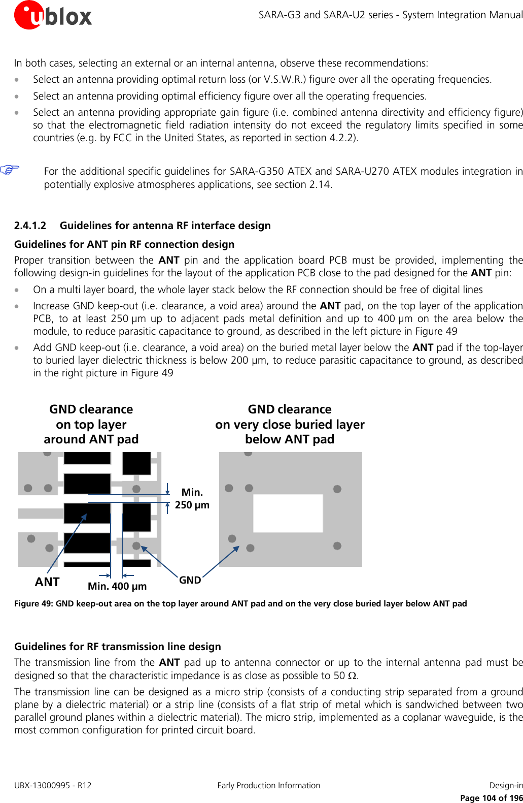
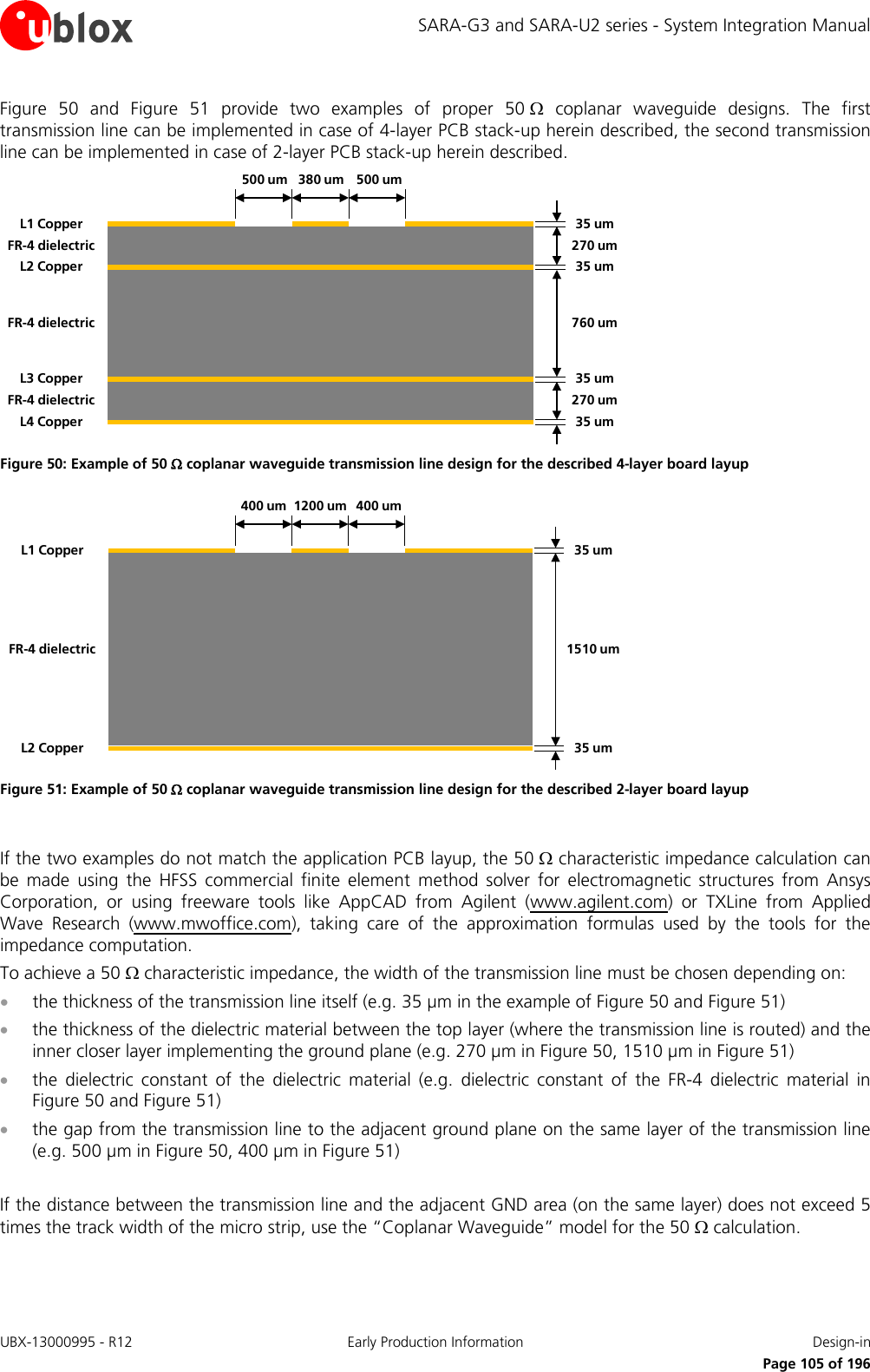
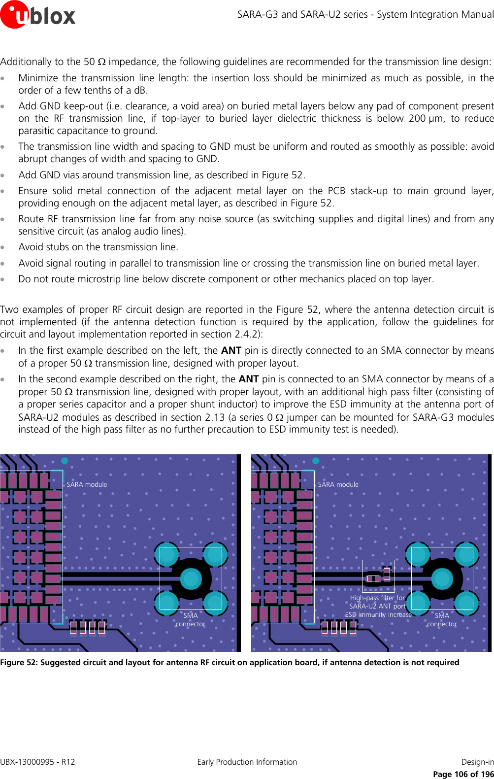
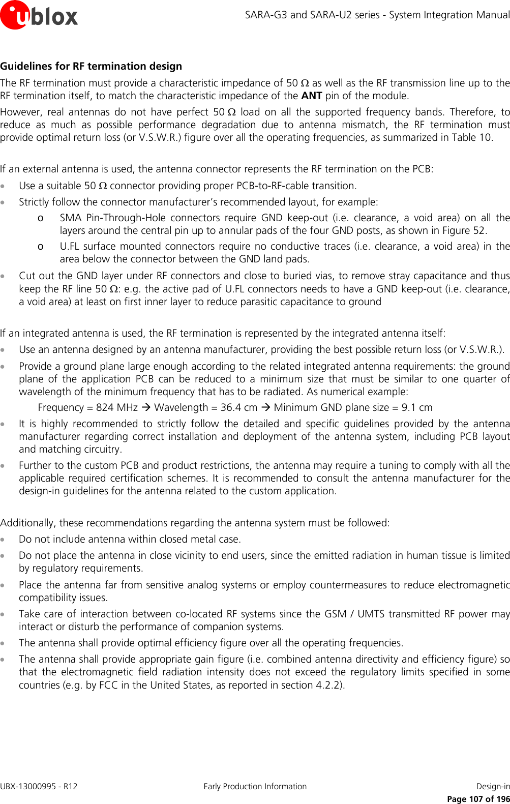
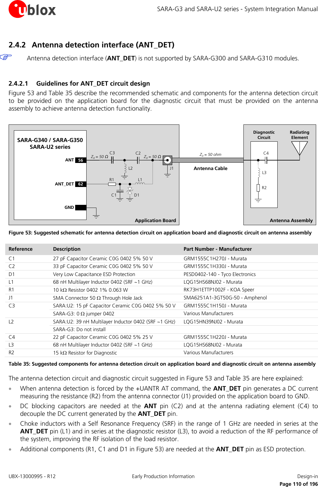
![SARA-G3 and SARA-U2 series - System Integration Manual • Additional high pass filter (C3 and L2 in Figure 53) is provided at the ANT pin as ESD immunity improvement for SARA-U2 modules (a series 0 Ω jumper can be mounted for SARA-G340 and SARA-G350 modules instead of the high pass filter, as no further precaution to ESD immunity test is needed). • The ANT pin must be connected to the antenna connector by means of a transmission line with nominal characteristics impedance as close as possible to 50 Ω. The DC impedance at RF port for some antennas may be a DC open (e.g. linear monopole) or a DC short to reference GND (e.g. PIFA antenna). For those antennas, without the diagnostic circuit of Figure 53, the measured DC resistance is always at the limits of the measurement range (respectively open or short), and there is no mean to distinguish between a defect on antenna path with similar characteristics (respectively: removal of linear antenna or RF cable shorted to GND for PIFA antenna). Furthermore, any other DC signal injected to the RF connection from ANT connector to radiating element will alter the measurement and produce invalid results for antenna detection. It is recommended to use an antenna with a built-in diagnostic resistor in the range from 5 kΩ to 30 kΩ to assure good antenna detection functionality and avoid a reduction of module RF performance. The choke inductor should exhibit a parallel Self Resonance Frequency (SRF) in the range of 1 GHz to improve the RF isolation of load resistor. For example: Consider an antenna with built-in DC load resistor of 15 kΩ. Using the +UANTR AT command, the module reports the resistance value evaluated from the antenna connector provided on the application board to GND: • Reported values close to the used diagnostic resistor nominal value (i.e. values from 13 kΩ to 17 kΩ if a 15 kΩ diagnostic resistor is used) indicate that the antenna is properly connected. • Values close to the measurement range maximum limit (approximately 50 kΩ) or an open-circuit “over range” report (see u-blox AT Commands Manual [3]) means that that the antenna is not connected or the RF cable is broken. • Reported values below the measurement range minimum limit (1 kΩ) highlights a short to GND at antenna or along the RF cable. • Measurement inside the valid measurement range and outside the expected range may indicate an improper connection, damaged antenna or wrong value of antenna load resistor for diagnostic. • Reported value could differ from the real resistance value of the diagnostic resistor mounted inside the antenna assembly due to antenna cable length, antenna cable capacity and the used measurement method. If the antenna detection function is not required by the customer application, the ANT_DET pin can be left not connected and the ANT pin can be directly connected to the antenna connector by means of a 50 Ω transmission line as described in Figure 52. UBX-13000995 - R12 Early Production Information Design-in Page 111 of 196](https://usermanual.wiki/u-blox/SARAU280/User-Guide-2520608-Page-111.png)
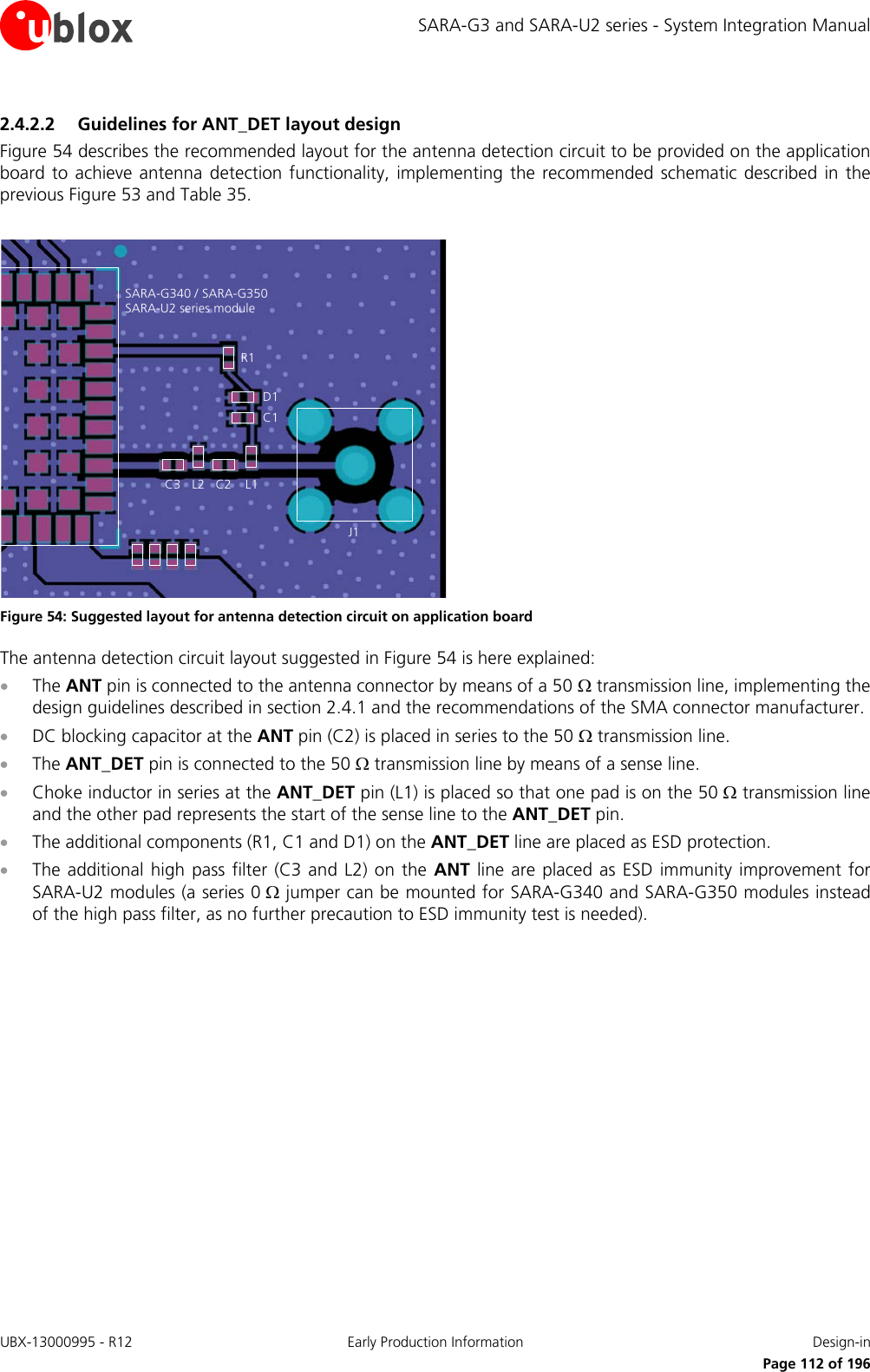
![SARA-G3 and SARA-U2 series - System Integration Manual Guidelines for dual SIM card / chip connection Two SIM card / chip can be connected to the modules’ SIM interface as described in the circuit of Figure 58. SARA-G3 and SARA-U2 modules do not support the usage of two SIM at the same time, but two SIM can be populated on the application board providing a proper switch to connect only the first SIM or only the second SIM per time to the SIM interface of the SARA-G3 and SARA-U2 modules as described in Figure 58. SARA-G3 modules do not support SIM hot insertion / removal: the module is able to properly use a SIM only if the SIM / module physical connection is provided before the module boot and then held for normal operation. Switching from one SIM to another one can only be properly done within one of these two time periods: • after module switch-off by the AT+CPWROFF and before module switch-on by PWR_ON • after network deregistration by AT+COPS=2 and before module reset by AT+CFUN=16 or RESET_N SARA-U2 modules support SIM hot insertion / removal on the SIM_DET pin: if the feature is enabled using the specific AT commands (refer to sections 1.8.2 and 1.11, and to the u-blox AT Commands Manual [3], +UGPIOC, +UDCONF commands), the switch from first SIM to the second SIM can be properly done when a Low logic level is present on the SIM_DET pin (‘SIM not inserted’ = SIM interface not enabled), without the necessity of a module re-boot, so that the SIM interface will be re-enabled by the module to use the second SIM when an High logic level will be re-applied on the SIM_DET pin. In the application circuit example represented in Figure 58, the application processor will drive the SIM switch using its own GPIO to properly select the SIM that is used by the module. Another GPIO may be used to handle the SIM hot insertion / removal function of SARA-U2 modules, which can also be handled by other external circuits or by the cellular module GPIO according to the application requirements. The dual SIM connection circuit described in Figure 58 can be implemented for SIM chips as well, providing proper connection between SIM switch and SIM chip as described in Figure 56. If it is required to switch between more than two SIMs, a circuit similar to the one described in Figure 58 can be implemented: for example, in case of four SIM circuit, using a proper 4-pole 4-throw switch (or, alternatively, four 1-pole 4-throw switches) instead of the suggested 4-pole 2-throw switch. Follow these guidelines connecting the module to two SIM connectors: • Use a proper low on resistance (i.e. few ohms) and low on capacitance (i.e. few pF) 2-throw analog switch (e.g. Fairchild FSA2567) as SIM switch to ensure high-speed data transfer according to SIM requirements. • Connect the contacts C1 (VCC) and C6 (VPP) of the two UICC / SIM to the VSIM pin of the module by means of a proper 2-throw analog switch (e.g. Fairchild FSA2567). • Connect the contact C7 (I/O) of the two UICC / SIM to the SIM_IO pin of the module by means of a proper 2-throw analog switch (e.g. Fairchild FSA2567). • Connect the contact C3 (CLK) of the two UICC / SIM to the SIM_CLK pin of the module by means of a proper 2-throw analog switch (e.g. Fairchild FSA2567). • Connect the contact C2 (RST) of the two UICC / SIM to the SIM_RST pin of the module by means of a proper 2-throw analog switch (e.g. Fairchild FSA2567). • Connect the contact C5 (GND) of the two UICC / SIM to ground. • Provide a 100 nF bypass capacitor (e.g. Murata GRM155R71C104K) at the SIM supply line (VSIM), close to the related pad of the two SIM connectors, to prevent digital noise. • Provide a bypass capacitor of about 22 pF to 47 pF (e.g. Murata GRM1555C1H470J) on each SIM line (VSIM, SIM_CLK, SIM_IO, SIM_RST), very close to each related pad of the two SIM connectors, to prevent RF coupling especially in case the RF antenna is placed closer than 10 - 30 cm from the SIM card holders. • Provide a very low capacitance (i.e. less than 10 pF) ESD protection (e.g. Tyco Electronics PESD0402-140) on each externally accessible SIM line, close to each related pad of the two SIM connectors, according to the EMC/ESD requirements of the custom application. • Limit capacitance and series resistance on each SIM signal (SIM_CLK, SIM_IO, SIM_RST) to match the requirements for the SIM interface (27.7 ns is the maximum allowed rise time on the SIM_CLK line, 1.0 µs is the maximum allowed rise time on the SIM_IO and SIM_RST lines). UBX-13000995 - R12 Early Production Information Design-in Page 117 of 196](https://usermanual.wiki/u-blox/SARAU280/User-Guide-2520608-Page-117.png)
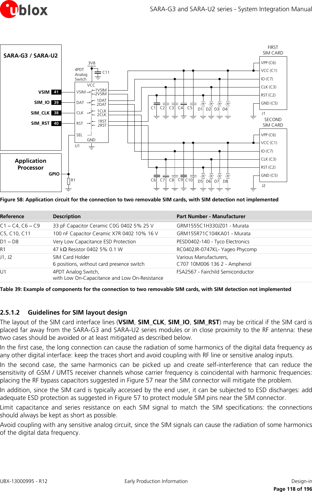
![SARA-G3 and SARA-U2 series - System Integration Manual 2.6 Serial interfaces 2.6.1 Asynchronous serial interface (UART) 2.6.1.1 Guidelines for UART circuit design Providing the full RS-232 functionality (using the complete V.24 link) If RS-232 compatible signal levels are needed, two different external voltage translators (e.g. Maxim MAX3237E and Texas Instruments SN74AVC8T245PW) can be used to provide full RS-232 (9 lines) functionality. The Texas Instruments chip provides the translation from 1.8 V to 3.3 V and vice versa, while the Maxim chip provides the translation from 3.3 V to RS-232 compatible signal level and vice versa. If a 1.8 V Application Processor (DTE) is used and complete RS-232 functionality as per ITU Recommendation [10] is required in the DTE/DCE serial communication, then the complete 1.8 V UART interface of the module (DCE) must be connected to a 1.8 V DTE as described in Figure 59. TxDApplication Processor(1.8V DTE)RxDRTSCTSDTRDSRRIDCDGNDSARA-G3 / SARA-U2(1.8V DCE)12TXD9DTR13RXD10RTS11CTS6DSR7RI8DCDGND0ΩTP0ΩTP0ΩTP0ΩTP Figure 59: UART interface application circuit with complete V.24 link in DTE/DCE serial communication (1.8 V DTE) If a 3.0 V Application Processor (DTE) is used, then it is recommended to connect the 1.8 V UART interface of the module (DCE) by means of appropriate unidirectional voltage translators using the module V_INT output as 1.8 V supply for the voltage translators on the module side, as described in Figure 60. 4V_INTTxDApplication Processor(3.0V DTE)RxDRTSCTSDTRDSRRIDCDGNDSARA-G3 / SARA-U2(1.8V DCE)12 TXD9DTR13 RXD10 RTS11 CTS6DSR7RI8DCDGND1V8B1 A1GNDU1B3A3VCCBVCCAUnidirectionalVoltage TranslatorC1 C23V0DIR3DIR2 OEDIR1VCCB2 A2B4A4DIR41V8B1 A1GNDU2B3A3VCCBVCCAUnidirectionalVoltage TranslatorC3 C43V0DIR1DIR3 OEB2 A2B4A4DIR4DIR2TP0ΩTP0ΩTP0ΩTP0ΩTP Figure 60: UART interface application circuit with complete V.24 link in DTE/DCE serial communication (3.0 V DTE) Reference Description Part Number - Manufacturer C1, C2, C3, C4 100 nF Capacitor Ceramic X7R 0402 10% 16 V GRM155R61A104KA01 - Murata U1, U2 Unidirectional Voltage Translator SN74AVC4T774 - Texas Instruments Table 40: Component for UART application circuit with complete V.24 link in DTE/DCE serial communication (3.0 V DTE) UBX-13000995 - R12 Early Production Information Design-in Page 119 of 196](https://usermanual.wiki/u-blox/SARAU280/User-Guide-2520608-Page-119.png)
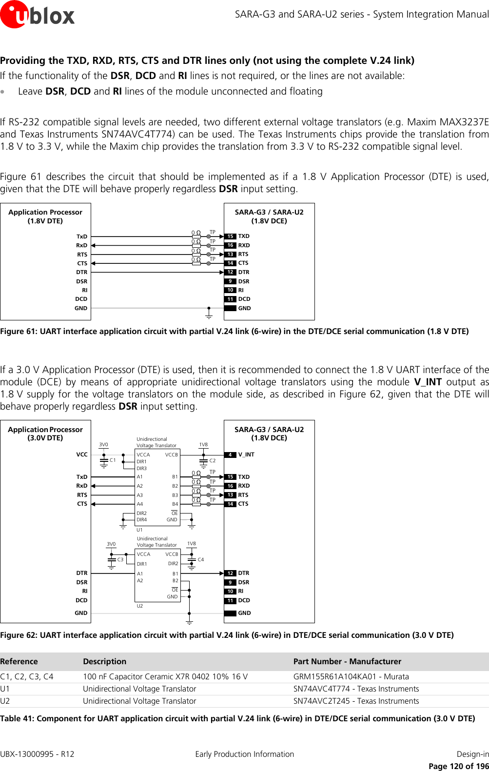
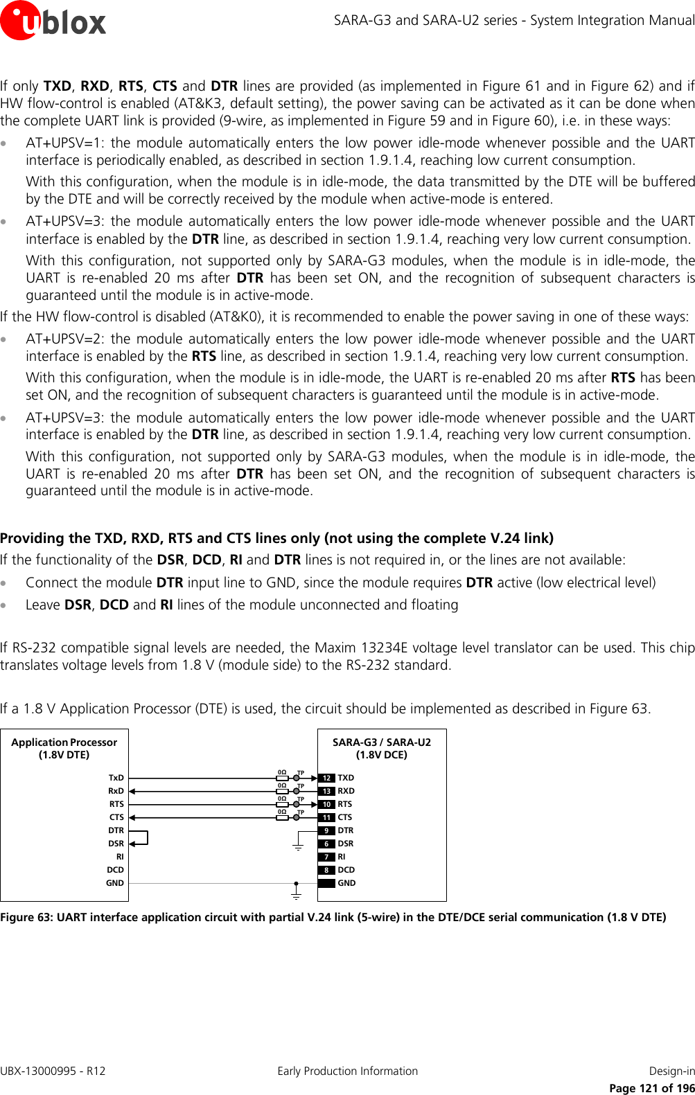
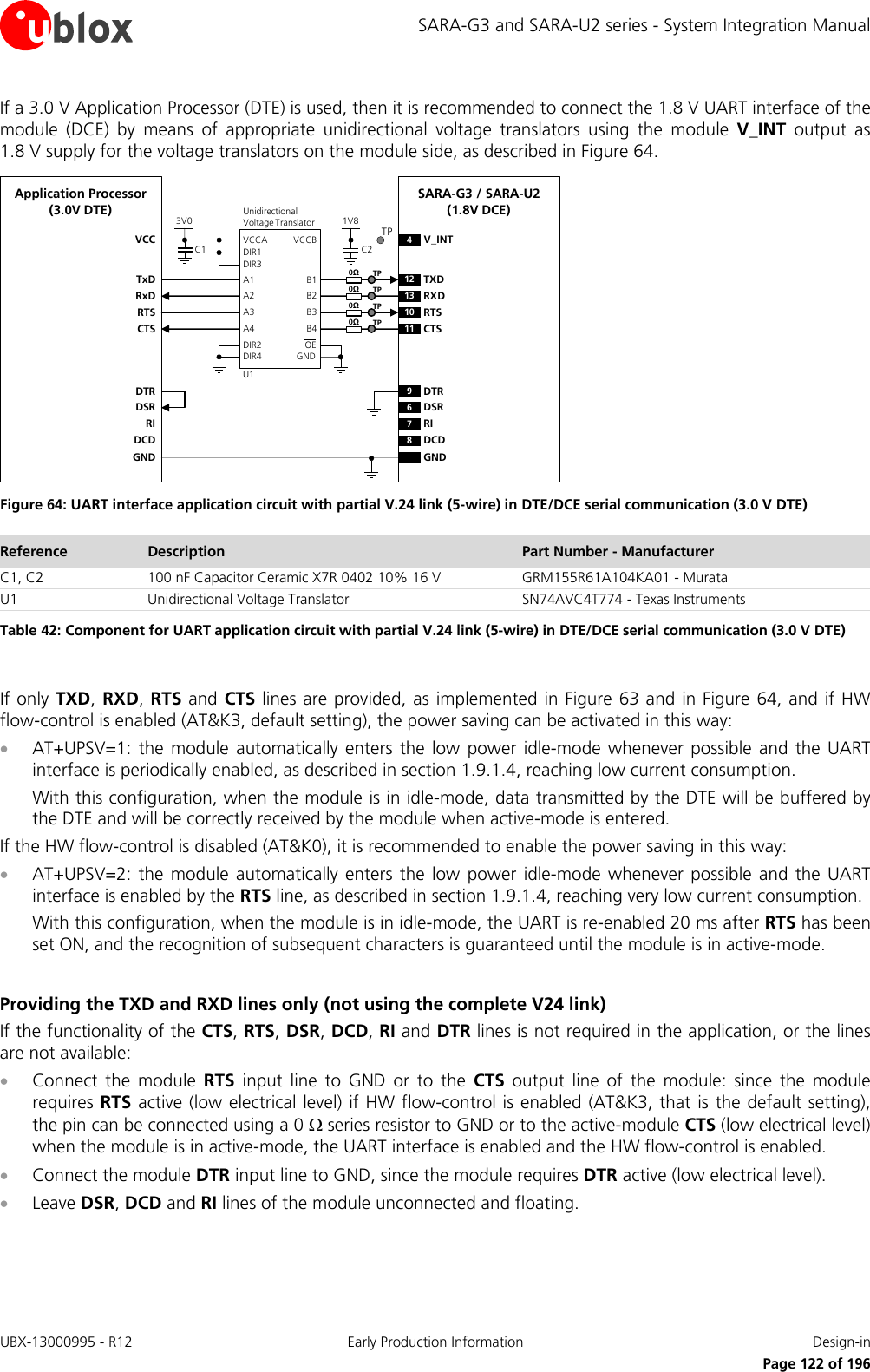
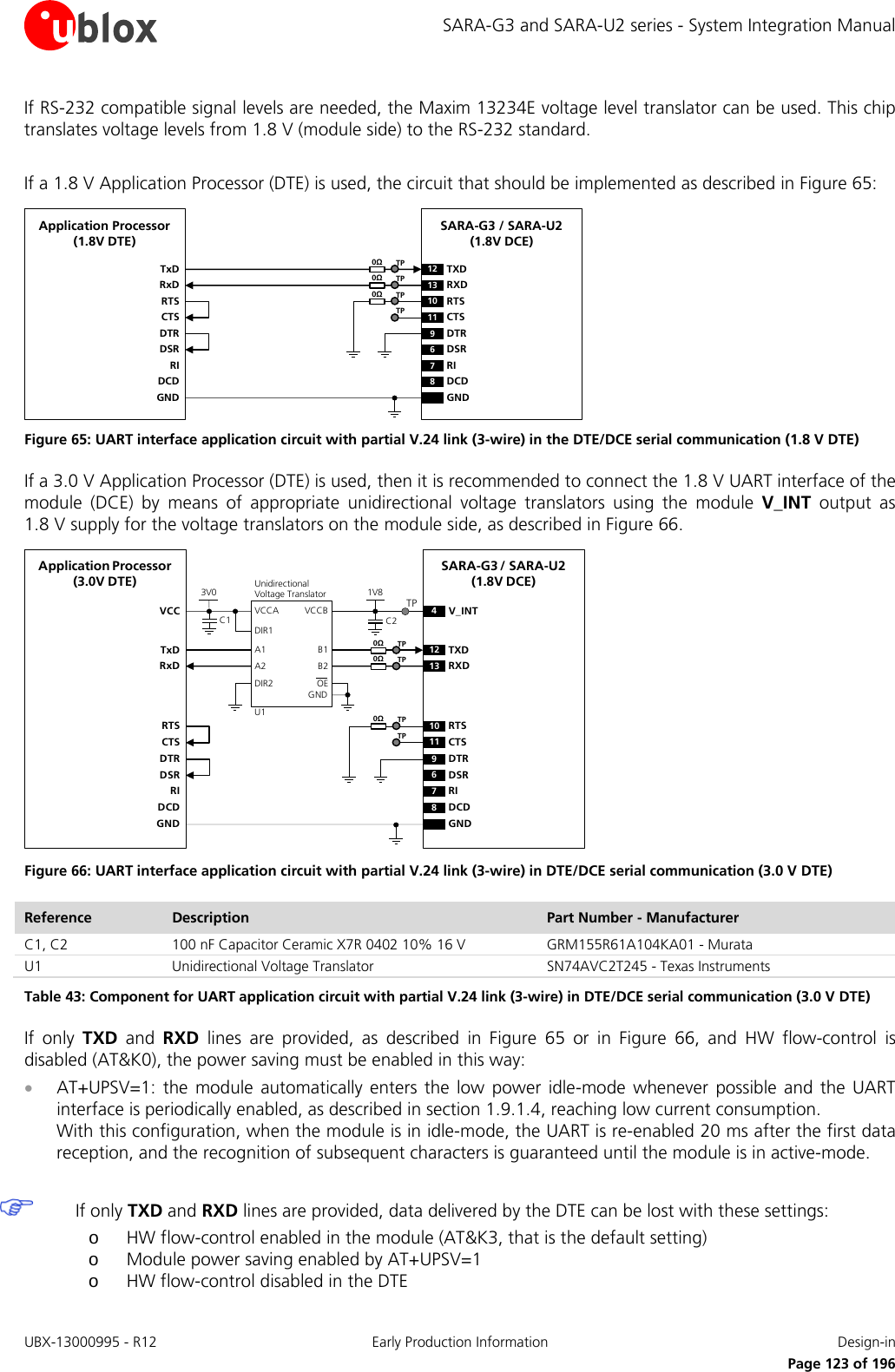
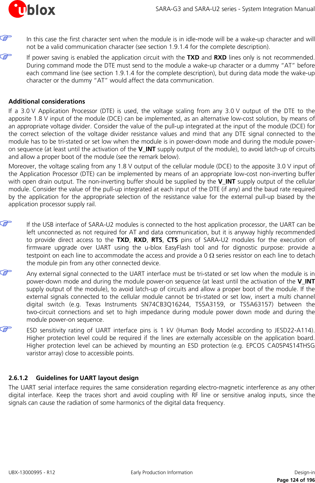
![SARA-G3 and SARA-U2 series - System Integration Manual 2.6.2 Auxiliary asynchronous serial interface (UART AUX) Auxiliary UART interface is not supported by SARA-U2 modules. 2.6.2.1 Guidelines for UART AUX circuit design The auxiliary UART interface can be connected to an application processor if it can be set in pass-through mode so that the auxiliary UART interface can be accessed for SARA-G3 modules’ firmware upgrade by means of the u-blox EasyFlash tool and for diagnostic purpose. It is highly recommended to provide direct access to the TXD_AUX, RXD_AUX pins of SARA-G3 modules for execution of firmware upgrade over auxiliary UART using the u-blox EasyFlash tool and for diagnostic purpose: provide a testpoint on each line to accommodate the access and provide a 0 Ω series resistor on each line to detach the module pin from any other connected device. The circuit with a 1.8 V application processor should be implemented as described in Figure 67. TxDApplication Processor(1.8V DTE)RxDSARA-G3 series (1.8V DCE)29TXD_AUX28RXD_AUXGND GND0 ohm0 ohmTestPointTestPoint Figure 67: UART AUX interface application circuit connecting a 1.8 V application processor If a 3.0 V application processor is used, then it is recommended to connect the 1.8 V auxiliary UART interface of the module by means of appropriate unidirectional voltage translators using the module V_INT output as 1.8 V supply for the voltage translators on the module side, as described in Figure 68. 4V_INTTxDApplication Processor(3.0V DTE)RxDGNDSARA-G3 series (1.8V DCE)29TXD_AUX28RXD_AUXGND1V8B1 A1GNDU1VCCBVCCAUnidirectionalVoltage TranslatorC1 C23V0DIR1DIR2OEVCCB2 A20 ohm0 ohmTPTPTP Figure 68: UART AUX interface application circuit connecting a 3.0 V application processor Reference Description Part Number - Manufacturer C1, C2 100 nF Capacitor Ceramic X7R 0402 10% 16 V GRM155R61A104KA01 - Murata U1 Unidirectional Voltage Translator SN74AVC2T245 - Texas Instruments Table 44: Component for UART AUX interface application circuit connecting a 3.0 V application processor See Firmware Update Application Note [25] for additional guidelines regarding the procedure for SARA-G3 modules’ firmware upgrade over the auxiliary UART interface using the u-blox EasyFlash tool. UBX-13000995 - R12 Early Production Information Design-in Page 125 of 196](https://usermanual.wiki/u-blox/SARAU280/User-Guide-2520608-Page-125.png)
![SARA-G3 and SARA-U2 series - System Integration Manual 2.6.3 Universal Serial Bus (USB) USB interface is not supported by SARA-G3 modules. 2.6.3.1 Guidelines for USB circuit design The USB_D+ and USB_D- lines carry the USB serial data and signaling. The lines are used in single ended mode for full speed signaling handshake, as well as in differential mode for high speed signaling and data transfer. USB pull-up or pull-down resistors on USB_D+ and USB_D- as required by the Universal Serial Bus Revision 2.0 specification [14] are part of the USB pin driver and do not need to be externally provided. Series resistors on USB_D+ and USB_D- as required by Universal Serial Bus Revision 2.0 specification [14] are also integrated and do not need to be externally provided. Since the module acts as a USB device, the VBUS USB supply (5.0 V typ.) generated by the USB host must be connected to the VUSB_DET input, which absorbs few microamperes to sense the host connection and enable the USB interface of the module. If connecting the USB_D+ and USB_D- pins to a USB device connector, the pin will be externally accessible on the application device. According to EMC/ESD requirements of the application, an additional ESD protection device with very low capacitance should be provided close to accessible point on the line connected to this pin, as described in Figure 69 and Table 45. The USB interface pins ESD sensitivity rating is 1 kV (Human Body Model according to JESD22-A114F). Higher protection level could be required if the lines are externally accessible and it can be achieved by mounting a very low capacitance (i.e. less or equal to 1 pF) ESD protection (e.g. Tyco Electronics PESD0402-140 ESD protection device) on the lines connected to these pins, close to accessible points. The USB pins of the modules can be directly connected to the USB host application processor without additional ESD protections if they are not externally accessible or according to EMC/ESD requirements. SARA-U2 series D+D-GND29USB_D+28USB_D-GNDUSB DEVICE CONNECTORD1 D2VBUSSARA-U2 series D+D-GND29USB_D+28USB_D-GNDUSB HOST PROCESSORC117VUSB_DETC117VUSB_DETVBUSD3 Figure 69: USB Interface application circuits Reference Description Part Number - Manufacturer C1 100 nF Capacitor Ceramic X7R 0402 10% 16 V GRM155R61A104KA01 - Murata D1, D2, D3 Very Low Capacitance ESD Protection PESD0402-140 - Tyco Electronics Table 45: Component for USB application circuits If the USB interface is not required by the customer application, as the UART interface is used for AT and data communication with the host application processor, the USB pins can be left unconnected, but it is highly recommended providing direct access on the application board by means of accessible testpoint directly connected to the VUSB_DET, USB_D+, USB_D- pins of SARA-U2 modules. UBX-13000995 - R12 Early Production Information Design-in Page 127 of 196](https://usermanual.wiki/u-blox/SARAU280/User-Guide-2520608-Page-127.png)
![SARA-G3 and SARA-U2 series - System Integration Manual 2.6.3.2 Guidelines for USB layout design The USB_D+ / USB_D- lines require accurate layout design to achieve reliable signaling at the high speed data rate (up to 480 Mb/s) supported by the USB serial interface. The characteristic impedance of the USB_D+ / USB_D- lines is specified by the Universal Serial Bus Revision 2.0 specification [14]. The most important parameter is the differential characteristic impedance applicable for the odd-mode electromagnetic field, which should be as close as possible to 90 Ω differential. Signal integrity may be degraded if PCB layout is not optimal, especially when the USB signaling lines are very long. Use the following general routing guidelines to minimize signal quality problems: • Route USB_D+ / USB_D- lines as a differential pair. • Route USB_D+ / USB_D- lines as short as possible. • Ensure the differential characteristic impedance (Z0) is as close as possible to 90 Ω. • Ensure the common mode characteristic impedance (ZCM) is as close as possible to 30 Ω. • Consider design rules for USB_D+ / USB_D- similar to RF transmission lines, being them coupled differential micro-strip or buried stripline: avoid any stubs, abrupt change of layout, and route on clear PCB area. • Avoid coupling with any RF line or sensitive analog inputs, since the signals can cause the radiation of some harmonics of the digital data frequency. Figure 70 and Figure 71 provide two examples of coplanar waveguide designs with differential characteristic impedance close to 90 Ω and common mode characteristic impedance close to 30 Ω. The first transmission line can be implemented in case of 4-layer PCB stack-up herein described, the second transmission line can be implemented in case of 2-layer PCB stack-up herein described. 35 µm35 µm35 µm35 µm270 µm270 µm760 µmL1 CopperL3 CopperL2 CopperL4 CopperFR-4 dielectricFR-4 dielectricFR-4 dielectric350 µm 400 µm400 µm350 µm400 µm Figure 70: Example of USB line design, with Z0 close to 90 Ω and ZCM close to 30 Ω, for the described 4-layer board layup 35 µm35 µm1510 µmL2 CopperL1 CopperFR-4 dielectric740 µm 410 µm410 µm740 µm410 µm Figure 71: Example of USB line design, with Z0 close to 90 Ω and ZCM close to 30 Ω, for the described 2-layer board layup UBX-13000995 - R12 Early Production Information Design-in Page 128 of 196](https://usermanual.wiki/u-blox/SARAU280/User-Guide-2520608-Page-128.png)
![SARA-G3 and SARA-U2 series - System Integration Manual 2.6.4 DDC (I2C) interface DDC (I2C) interface is not supported by SARA-G300 and SARA-G310 modules. 2.6.4.1 Guidelines for DDC (I2C) circuit design General considerations The DDC I2C-bus master interface of SARA-G340, SARA-G350 and SARA-U2 cellular modules can be used to communicate with u-blox GNSS receivers and, on SARA-U2 modules only, it can be also used to communicate with other external I2C-bus slaves as an audio codec. Beside the general considerations reported below, see: • the following parts of this section for specific guidelines for the connection to u-blox GNSS receivers. • the section 2.7.2 for an application circuit example with an external audio codec I2C-bus slave. To be compliant to the I2C-bus specifications, the module bus interface pins are open drain output and pull up resistors must be mounted externally. Resistor values must conform to I2C bus specifications [15]: for example, 4.7 kΩ resistors can be commonly used. Connect the external DDC (I2C) pull-ups to the V_INT 1.8 V supply source, or another supply source enabled after V_INT (e.g., as the GNSS 1.8 V supply present in Figure 72 application circuit), as any external signal connected to the DDC (I2C) interface must not be set high before the switch-on of the V_INT supply of the DDC (I2C) pins, to avoid latch-up of circuits and let a proper boot of the module. The signal shape is defined by the values of the pull-up resistors and the bus capacitance. Long wires on the bus increase the capacitance. If the bus capacitance is increased, use pull-up resistors with nominal resistance value lower than 4.7 kΩ, to match the I2C bus specifications [15] regarding rise and fall times of the signals. Capacitance and series resistance must be limited on the bus to match the I2C specifications (1.0 µs is the maximum allowed rise time on the SCL and SDA lines): route connections as short as possible. ESD sensitivity rating of the DDC (I2C) pins is 1 kV (Human Body Model according to JESD22-A114). Higher protection level could be required if the lines are externally accessible and it can be achieved by mounting an ESD protection (e.g. EPCOS CA05P4S14THSG varistor array) close to accessible points. If the pins are not used as DDC bus interface, they can be left unconnected. UBX-13000995 - R12 Early Production Information Design-in Page 129 of 196](https://usermanual.wiki/u-blox/SARAU280/User-Guide-2520608-Page-129.png)
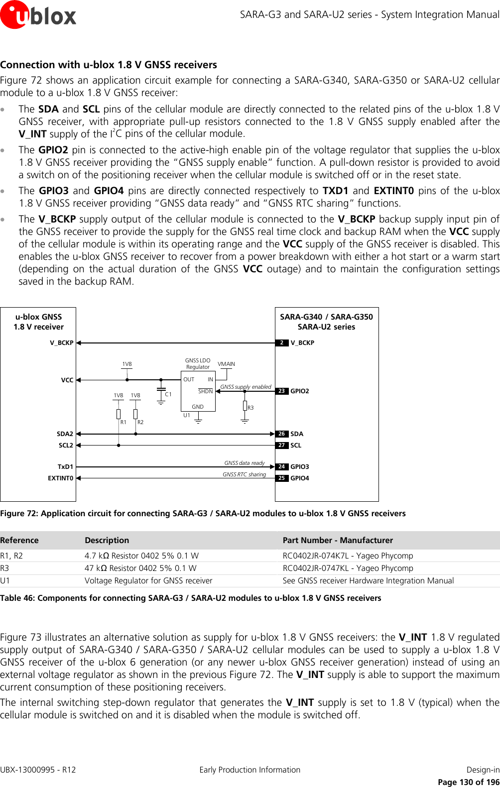
![SARA-G3 and SARA-U2 series - System Integration Manual The supply of the u-blox 1.8 V GNSS receiver can be switched off using an external p-channel MOSFET controlled by the GPIO2 pin by means of a proper inverting transistor as shown in Figure 73, implementing the “GNSS supply enable” function. If this feature is not required, the V_INT supply output can be directly connected to the u-blox 1.8 V GNSS receiver, so that it will be switched on when V_INT output is enabled. The V_INT supply output provides low voltage ripple (up to 15 mVpp) when the module is in active-mode or in connected-mode, but it provides higher voltage ripple (up to 90 mVpp on SARA-G3 series, or up to 70 mVpp on SARA-U2 series) when the module is in the low power idle-mode with power saving configuration enabled by the AT+UPSV (see u-blox AT Commands Manual [3]). According to the voltage ripple characteristic of the V_INT supply output: • The power saving configuration cannot be enabled to use V_INT output to properly supply any 1.8 V GNSS receiver of the u-blox 6 generation and any 1.8 V GNSS receiver of the u-blox 7 generation or any newer u-blox GNSS receiver generation with TCXO. • The power saving configuration can be enabled to use V_INT output to properly supply any 1.8 V GNSS receiver of the u-blox 7 generation or any newer u-blox GNSS receiver generation without TCXO. • Additional filtering may be needed to properly supply an external LNA, depending on the characteristics of the used LNA, adding a series ferrite bead and a bypass capacitor (e.g. the Murata BLM15HD182SN1 ferrite bead and the Murata GRM1555C1H220J 22 pF capacitor) at the input of the external LNA supply line. SARA-G340 / SARA-G350SARA-U2 seriesu-blox GNSS1.8 V receiverTxD1EXTINT0GPIO3GPIO42425V_BCKP V_BCKP2SDA2SCL223 GPIO2SDASCL2627VCC1V8C1R34V_INTR5R4TPT2T1R1 R21V8 1V8GNSS data readyGNSS RTC sharingGNSS supply enabled Figure 73: Application circuit for connecting SARA-G3 / SARA-U2 modules to u-blox 1.8 V GNSS receivers using V_INT as supply Reference Description Part Number - Manufacturer R1, R2 4.7 kΩ Resistor 0402 5% 0.1 W RC0402JR-074K7L - Yageo Phycomp R3 47 kΩ Resistor 0402 5% 0.1 W RC0402JR-0747KL - Yageo Phycomp R4 10 kΩ Resistor 0402 5% 0.1 W RC0402JR-0710KL - Yageo Phycomp R5 100 kΩ Resistor 0402 5% 0.1 W RC0402JR-07100KL - Yageo Phycomp T1 P-Channel MOSFET Low On-Resistance IRLML6401 - International Rectifier or NTZS3151P - ON Semi T2 NPN BJT Transistor BC847 - Infineon C1 100 nF Capacitor Ceramic X7R 0402 10% 16 V GRM155R71C104KA01 - Murata Table 47: Components for connecting SARA-G3 / SARA-U2 modules to u-blox 1.8 V GNSS receivers using V_INT as supply For additional guidelines regarding the design of applications with u-blox 1.8 V GNSS receivers see the GNSS Implementation Application Note [24] and to the Hardware Integration Manual of the u-blox GNSS receivers. UBX-13000995 - R12 Early Production Information Design-in Page 131 of 196](https://usermanual.wiki/u-blox/SARAU280/User-Guide-2520608-Page-131.png)
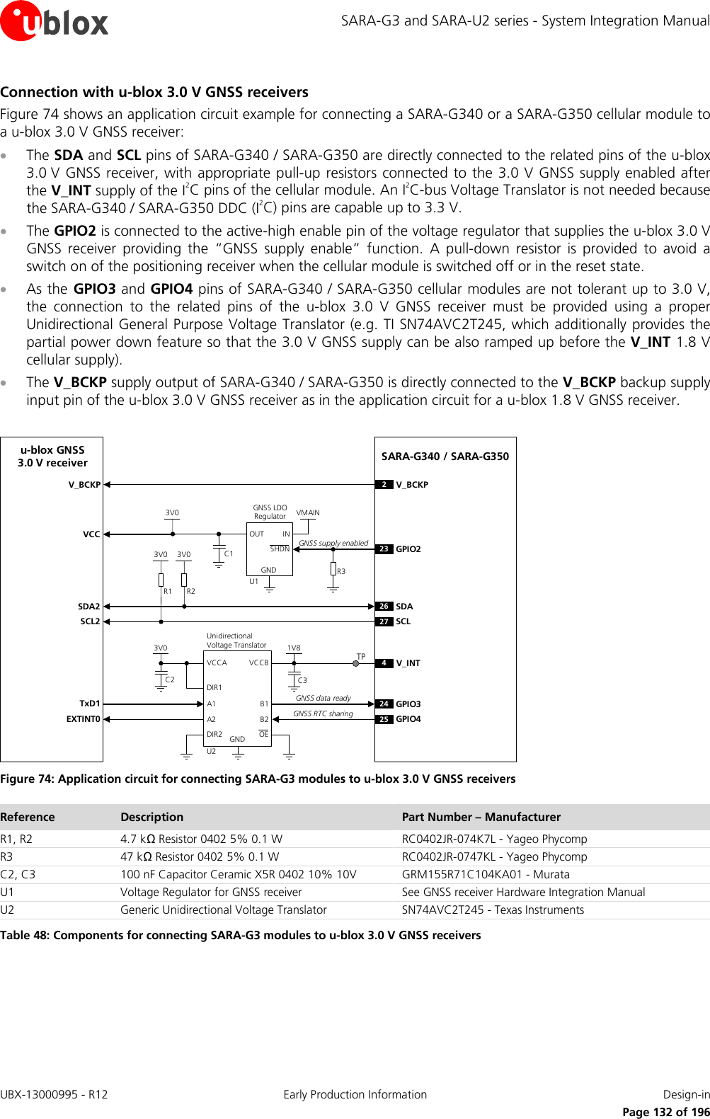
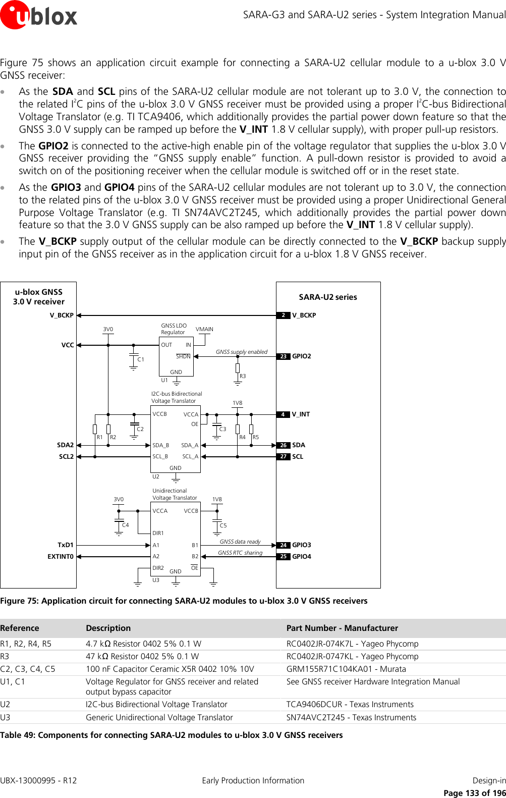
![SARA-G3 and SARA-U2 series - System Integration Manual For additional guidelines regarding the design of applications with u-blox 3.0 V GNSS receivers see the GNSS Implementation Application Note [24] and to the Hardware Integration Manual of the u-blox GNSS receivers. 2.6.4.2 Guidelines for DDC (I2C) layout design The DDC (I2C) serial interface requires the same consideration regarding electro-magnetic interference as any other digital interface. Keep the traces short and avoid coupling with RF line or sensitive analog inputs, since the signals can cause the radiation of some harmonics of the digital data frequency. UBX-13000995 - R12 Early Production Information Design-in Page 134 of 196](https://usermanual.wiki/u-blox/SARAU280/User-Guide-2520608-Page-134.png)
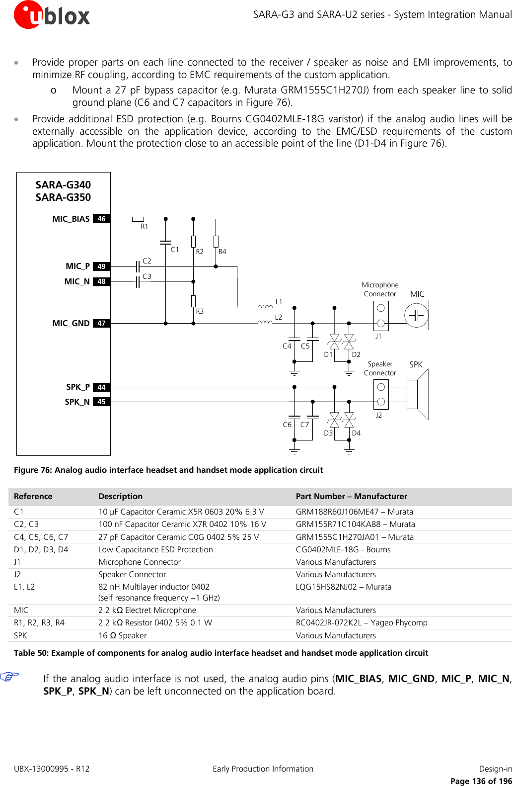
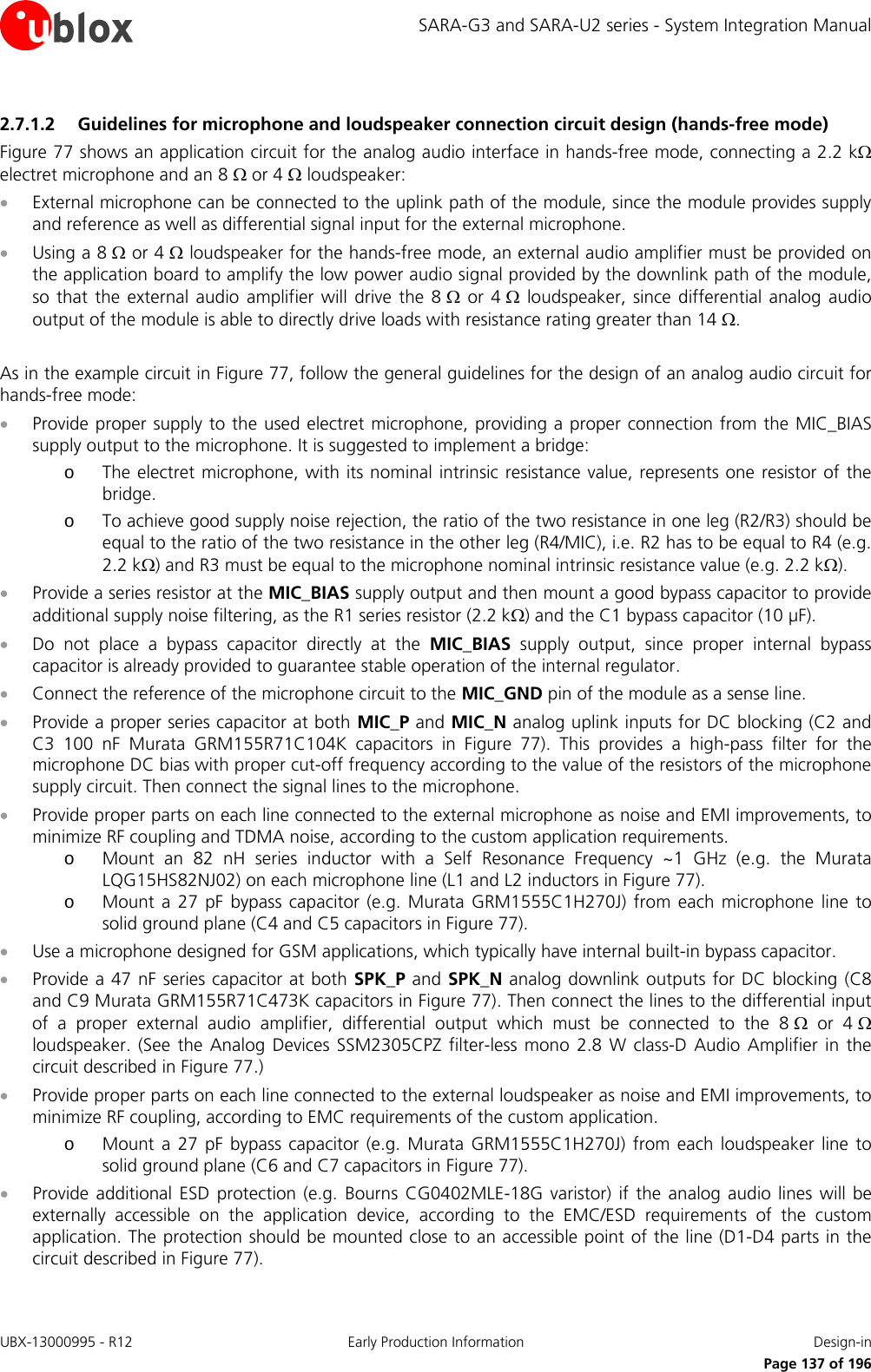
![SARA-G3 and SARA-U2 series - System Integration Manual 2.7.1.3 Guidelines for external analog audio device connection circuit design The differential analog audio I/O can be used to connect the module to an external analog audio device. Audio devices with a differential analog I/O are preferable, as they are more immune to external disturbances. Figure 78 and Table 52 describe the application circuits, following the suggested circuit design-in. Guidelines for the connection to a differential analog audio input: • The SPK_P / SPK_N balanced output of the module must be connected to the differential input of the external audio device by means of series capacitors for DC blocking (e.g. 10 µF) to decouple the bias present at the module output, as described in the left side of Figure 78. Guidelines for the connection to a single ended analog audio input: • A proper differential to single ended circuit must be inserted from the SPK_P / SPK_N balanced output of the module to the single ended input of the external audio device, as described in the Figure 78 right side: 10 µF series capacitors are provided to decouple the bias present at the module output, and a voltage divider is provided to properly adapt the signal level from module output to external audio device input. Guidelines for the connection to a differential analog audio output: • The MIC_P / MIC_N balanced input of the module must be connected to the differential output of the external audio device by means of series capacitors for DC blocking (e.g. 10 µF) to decouple the bias present at the module input, as described in the Figure 78 left side. Guidelines for the connection to a single ended analog audio output: • A proper single ended to differential circuit has to be inserted from the single ended output of the external audio device to the MIC_P / MIC_N balanced input of the module, as described in the Figure 78 right side: 10 µF series capacitors are provided to decouple the bias present at the module input, and a voltage divider is provided to properly adapt the signal level from the external device output to the module input. Additional guidelines for any connection: • The DC-block series capacitor acts as high-pass filter for audio signals, with cut-off frequency depending on both the values of capacitor and on the input impedance of the device. For example: in case of differential input impedance of 600 Ω , the two 10 µF capacitors will set the -3 dB cut-off frequency to 53 Hz, while for single ended connection to 600 Ω external device, the cut-off frequency with just the single 10 µF capacitor will be 103 Hz. In both cases the high-pass filter has a low enough cut-off for proper frequency response. • Use a suitable power-on sequence to avoid audio bump due to charging of the capacitor: the final audio stage should be always enabled as last one. • The signal levels can be adapted by setting gain using AT commands (see u-blox AT Commands Manual [3], +USGC, +UMGC), but additional circuitry must be inserted if SPK_P / SPK_N output level of the module is too high for the audio device input or if the audio device output level is too high for MIC_P / MIC_N, as the voltage dividers present in the circuits described in Figure 78 right side to properly adapt the signal level. SARA-G340 SARA-G350C1C245SPK_N44SPK_PGND49MIC_PGNDAnalog IN (-)Analog IN (+)Analog OUT (-)Analog OUT (+)Audio DeviceGNDGND48MIC_NC3C4SARA-G340 SARA-G35045SPK_N44SPK_PGND49MIC_PGNDAnalog INAudio DeviceGNDReference48MIC_NAnalog OUTC5C6 R2R1R4R3C7C846MIC_BIAS47MIC_GND46MIC_BIAS47MIC_GND Figure 78: Application circuits to connect the module to audio devices with proper differential or single-ended input/output UBX-13000995 - R12 Early Production Information Design-in Page 139 of 196](https://usermanual.wiki/u-blox/SARAU280/User-Guide-2520608-Page-139.png)
![SARA-G3 and SARA-U2 series - System Integration Manual 2.7.2 Digital audio interface SARA-G300 and SARA-G310 modules do not provide digital audio interface. 2.7.2.1 Guidelines for digital audio circuit design The I2S digital audio interface of SARA-G3 and SARA-U2 series modules can be connected to an external digital audio device for voice applications. Any external digital audio device compliant to the configuration of the digital audio interface of the cellular module can be used, given that the external digital audio device has to provide: • The opposite role: slave for SARA-G3 modules that act as master only; slave or master for SARA-U2 modules that may act as master or slave • The same mode and frame format: PCM / short alignment or Normal I2S mode / long alignment mode with o data in 2’s complement notation o MSB transmitted first o word length = 16-bit o frame length = 17-bit or 18-bit in PCM / short alignment mode (16 + 1 or 16 + 2 clock cycles, with Word Aligment / Synchronization signal set high for 1 clock cycle or 2 clock cycles), or o frame length = 32-bit in Normal I2S mode / long alignment mode (16 x 2 clock cycles) • The same sample rate and serial clock frequency: as the clock frequency depends on the frame length and the sample rate, the clock frequency can be o 17 x <I2S_sample_rate> or 18 x <I2S_sample_rate> in PCM / short alignment mode, or o 16 x 2 x <I2S_sample_rate> in Normal I2S mode / long alignment mode • Compatible voltage levels (1.80 V typ.), otherwise it is recommended to connect the 1.8 V digital audio interface of the module to the external 3.0 V (or similar) digital audio device by means of appropriate unidirectional voltage translators (e.g. Texas Instruments SN74AVC4T774 or SN74AVC2T245), using the module V_INT output as 1.8 V supply for the voltage translators on the module side For the appropriate selection of a compliant external digital audio device, see the section 1.10.2 including subsections 1.10.2.1 and 1.10.2.2. See the +UI2S AT command description in the u-blox AT Commands Manual [3] for further details regarding the capabilities and the possible settings of I2S digital audio interface of SARA-G3 and SARA-U2 series modules. Figure 79 and Table 53 describe an application circuit example for the I2S digital audio interface of SARA-U2 modules providing voice capability using an external audio voice codec. DAC and ADC integrated in the external audio codec respectively converts an incoming digital data stream to analog audio output through a mono amplifier and converts the microphone input signal to the digital bit stream over the digital audio interface. • The module’s I2S interface (I2S master) is connected to the related pins of the external audio codec (I2S slave). • The V_INT output supplies the external audio codec, defining proper digital interfaces voltage level. • The external audio codec is controlled by the SARA-U2 module using the DDC (I2C) interface: this interface can be concurrently used to communicate with u-blox GNSS receivers and with an external audio codec. • The CODEC_CLK pin of the SARA-U2 module (that provides a suitable digital output clock) is connected to the clock input of the external audio codec to provide clock reference. • Additional components are provided for EMC and ESD immunity conformity: a 10 nF bypass capacitor and a series chip ferrite bead noise/EMI suppression filter provided on each microphone line input and speaker line output of the external codec as described in Figure 79 and Table 53. The necessity of these or other additional parts for EMC improvement may depend on the specific application board design. UBX-13000995 - R12 Early Production Information Design-in Page 141 of 196](https://usermanual.wiki/u-blox/SARAU280/User-Guide-2520608-Page-141.png)
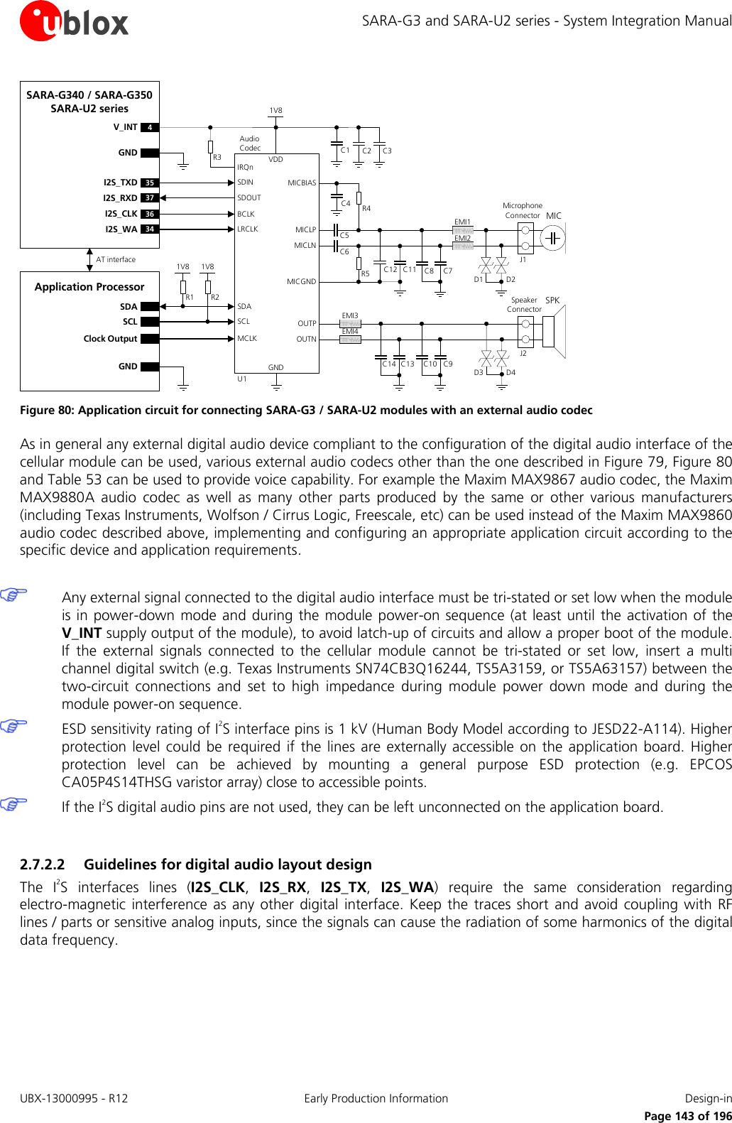
![SARA-G3 and SARA-U2 series - System Integration Manual 2.12 Thermal guidelines SARA-G3 and SARA-U2 series module operating temperature range and module thermal resistance are specified in the SARA-G3 series Data Sheet [1] or the SARA-U2 series Data Sheet [2]. The most critical condition concerning module thermal performance is the uplink transmission at maximum power (data upload or voice call in connected-mode), when the baseband processor runs at full speed, radio circuits are all active and the RF power amplifier is driven to higher output RF power. This scenario is not often encountered in real networks; however the application should be correctly designed to cope with it. During transmission at maximum RF power the SARA-G3 modules generate thermal power that can exceed 1 W, whereas the SARA-U2 modules generate thermal power that can exceed 2 W: these are indicative values since the exact generated power strictly depends on operating condition such as the cellular radio access technology, the number of allocated TX slot, the transmitting frequency band, etc. The generated thermal power must be adequately dissipated through the thermal and mechanical design of the application, in particular for SARA-U2 modules when operating in the 3G cellular radio access technology. SARA-U2 modules implement an integrated self protection algorithm when operating in the 3G cellular radio access technology: the module reduces the transmitted power when the temperature internally sensed in the integrated 3G Power Amplifier approaches the maximum allowed internal temperature, to guarantee device functionality and long life span. The spreading of the Module-to-Ambient thermal resistance (Rth,M-A) depends on module operating condition: the overall temperature distribution is influenced by the configuration of the active components during the specific mode of operation and their different thermal resistance toward the case interface. Mounting a SARA-G3 module on a 79 mm x 62 mm x 1.41 mm 4-Layers PCB with a high coverage of copper in still air conditions11, the increase of the module temperature12 in different modes of operation, referred to idle state initial condition13, can be summarized as following: • ~8 °C during a GSM voice call (1 TX slot, 1 RX slot) at max TX power • ~12 °C during a GPRS data transfer (2 TX slots, 3 RX slots) at max TX power The Module-to-Ambient thermal resistance value and the relative increase of module temperature are application dependent, according to the specific mechanical deployment of the module, e.g. application PCB dimensions and characteristics, mechanical shells enclosure and air flow conditions. The increase of thermal dissipation, i.e. the Module-to-Ambient thermal resistance reduction, will decrease the temperature for internal circuitry of the SARA-G3 and SARA-U2 series modules for a given operating ambient temperature. This improves device long-term reliability for applications operating at high ambient temperature. A few hardware techniques may be used to reduce the Module-to-Ambient thermal resistance in the application: • Connect each GND pin with solid ground layer of the application board and connect each ground area of the multilayer application board with complete via stack down to main ground layer • Provide a ground plane as wide as possible on the application board • Optimize antenna return loss, to optimize overall electrical performance of the module including a decrease of module thermal power 11 Refer to SARA-G3 and SARA-U2 series Data Sheet [1] for the Rth,M-A value in this application condition 12 Temperature is measured by internal sensor of cellular module 13 Steady state thermal equilibrium is assumed. The module’s temperature in idle state can be considered equal to ambient temperature UBX-13000995 - R12 Early Production Information Design-in Page 147 of 196](https://usermanual.wiki/u-blox/SARAU280/User-Guide-2520608-Page-147.png)
![SARA-G3 and SARA-U2 series - System Integration Manual • Optimize the thermal design of any high-power component included in the application, as linear regulators and amplifiers, to optimize overall temperature distribution in the application device • Select the material, the thickness and the surface of the box (i.e. the mechanical enclosure of the application device that integrates the module) so that it provides good thermal dissipation • Force ventilation air-flow within mechanical enclosure • Provide a heat sink component attached to the module top side, with electrically insulated / high thermal conductivity adhesive, or on the backside of the application board, below the cellular module, as a large part of the heat is transported through the GND pads and dissipated over the backside of the application board For example, after the installation of a robust aluminum heat-sink with forced air ventilation on the back of the same application board described above, the Module-to-Ambient thermal resistance (Rth,M-A) is reduced up to the Module-to-Case thermal resistance (Rth,M-C) defined in the SARA-G3 series Data Sheet [1] or the SARA-U2 series Data Sheet [2]. The effect of lower Rth,M-A due to the installation of a robust heat-sink on the backside of the application board with forced air ventilation can be seen from the module temperature increase, which now can be summarized as following for SARA-G3 modules: • ~1 °C during a GSM voice call (1 TX slot, 1 RX slot) at the maximum TX power • ~2 °C during a GPRS data transfer (2 TX slots, 3 RX slots) at the maximum TX power Beside the reduction of the Module-to-Ambient thermal resistance implemented by the hardware design of the application device integrating a SARA-G3 and SARA-U2 series module, the increase of module temperature can be moderated by the software implementation of the application. Since the most critical condition concerning module thermal power occurs when module connected-mode is enabled, the actual module thermal power depends, as module current consumption, on the radio access mode, the operating band and the average TX power. A few software techniques may be implemented to reduce the module temperature increase in the application: • Select the radio access mode which provides lower temperature increase by means of AT command (see the u-blox AT Commands Manual [3]) • Select by means of AT command the GPRS multi-slot class which provides lower current consumption (see current consumption values reported in SARA-G3 series Data Sheet [1] or SARA-U2 series Data Sheet [2], and u-blox AT Commands Manual [3], +UCLASS command) • Select by means of AT command the operating band which provides lower current consumption (see current consumption values reported in SARA-G3 series Data Sheet [1] or SARA-U2 series Data Sheet [2], and u-blox AT Commands Manual [3], +UBANDSEL command) • Enable module connected-mode for a given time period and then disable it for a time period enough long to properly mitigate temperature increase UBX-13000995 - R12 Early Production Information Design-in Page 148 of 196](https://usermanual.wiki/u-blox/SARAU280/User-Guide-2520608-Page-148.png)
![SARA-G3 and SARA-U2 series - System Integration Manual 2.13 ESD guidelines The sections 2.13.1 and 2.13.2 are related to EMC / ESD immunity, herein described in section 2.13.1. The modules are ESD sensitive devices and the ESD sensitivity for each pin (as Human Body Model according to JESD22-A114F) is specified in SARA-G3 series Data Sheet [1] or SARA-U2 series Data Sheet [2], requiring special precautions when handling: for ESD handling guidelines see section 3.2. 2.13.1 ESD immunity test overview The immunity of devices integrating SARA-G3 and SARA-U2 series modules to Electro-Static Discharge (ESD) is part of the Electro-Magnetic Compatibility (EMC) conformity, which is required for products bearing the CE marking, compliant with the R&TTE Directive (99/5/EC), the EMC Directive (89/336/EEC) and the Low Voltage Directive (73/23/EEC) issued by the Commission of the European Community. Compliance with these directives implies conformity to the following European Norms for device ESD immunity: ESD testing standard CENELEC EN 61000-4-2 [18] and the radio equipment standards ETSI EN 301 489-1 [19], ETSI EN 301 489-7 [20], ETSI EN 301 489-24 [21], which requirements are summarized in Table 56. The ESD immunity test is performed at the enclosure port, defined by ETSI EN 301 489-1 [19] as the physical boundary through which the electromagnetic field radiates. If the device implements an integral antenna, the enclosure port is defined as all insulating and conductive surfaces housing the device. If the device implements a removable antenna, the antenna port can be separated from the enclosure port. The antenna port includes the antenna element and its interconnecting cable surfaces. The applicability of the ESD immunity test to the whole device depends on the device classification as defined by ETSI EN 301 489-1 [19]. Applicability of the ESD immunity test to the relative device ports or the relative interconnecting cables to auxiliary equipments, depends on device accessible interfaces and manufacturer requirements, as defined by ETSI EN 301 489-1 [19]. Contact discharges are performed at conductive surfaces, while air discharges are performed at insulating surfaces. Indirect contact discharges are performed on the measurement setup horizontal and vertical coupling planes as defined in CENELEC EN 61000-4-2 [18]. For the definition of integral antenna, removable antenna, antenna port, device classification see ETSI EN 301 489-1 [19], whereas for contact and air discharges definitions see CENELEC EN 61000-4-2 [18] Application Category Immunity Level All exposed surfaces of the radio equipment and ancillary equipment in a representative configuration Contact Discharge 4 kV Air Discharge 8 kV Table 56: EMC / ESD immunity requirements as defined by CENELEC EN 61000-4-2, ETSI EN 301 489-1, 301 489-7, 301 489-24 2.13.2 ESD immunity test of u-blox SARA-G3 and SARA-U2 reference designs EMC certification tests (including ESD immunity) have been successfully performed on the u-blox SARA-G3 and SARA-U2 reference designs according to applicable European Norms (see Table 56), as required for customized devices integrating the modules for R&TTED and European Conformance CE mark. The EMC / ESD approved u-blox reference designs consist of a SARA-G3 or a SARA-U2 module soldered onto a motherboard which provides supply interface, SIM card, headset and communication port. An external cellular antenna is connected to an SMA connector provided on the motherboard. Since an external antenna is used, the antenna port can be separated from the enclosure port. The reference design is not enclosed in a box so that the enclosure port is not indentified with physical surfaces. Therefore, some test cases cannot be applied. Only the antenna port is identified as accessible for direct ESD exposure. UBX-13000995 - R12 Early Production Information Design-in Page 149 of 196](https://usermanual.wiki/u-blox/SARAU280/User-Guide-2520608-Page-149.png)
![SARA-G3 and SARA-U2 series - System Integration Manual Table 57 reports the u-blox SARA-G3 and SARA-U2 reference designs ESD immunity test results, according to the CENELEC EN 61000-4-2 [18], ETSI EN 301 489-1 [19], 301 489-7 [20], 301 489-24 [21] test requirements. Category Application Immunity Level Remarks Contact Discharge to coupling planes (indirect contact discharge) Enclosure +4 kV / –4 kV Contact Discharges to conducted surfaces (direct contact discharge) Enclosure port Not Applicable Test not applicable to u-blox reference design because it does not provide enclosure surface. The test is applicable only to equipments providing conductive enclosure surface. Antenna port +4 kV / –4 kV Test applicable to u-blox reference design because it provides antenna with conductive & insulating surfaces. The test is applicable only to equipments providing antenna with conductive surface. Air Discharge at insulating surfaces Enclosure port Not Applicable Test not applicable to the u-blox reference design because it does not provide an enclosure surface. The test is applicable only to equipments providing insulating enclosure surface. Antenna port +8 kV / –8 kV Test applicable to u-blox reference design because it provides antenna with conductive & insulating surfaces. The test is applicable only to equipments providing antenna with insulating surface. Table 57: Enclosure ESD immunity level of u-blox SARA-G3 and SARA-U2 reference designs SARA-G3 and SARA-U2 reference designs implement all the ESD precautions described in section 2.13.3. 2.13.3 ESD application circuits The application circuits described in this section are recommended and should be implemented in any device that integrates a SARA-G3 and SARA-U2 series module, according to the application board classification (see ETSI EN 301 489-1 [19]), to satisfy the requirements for ESD immunity test summarized in Table 56. Antenna interface The ANT pin of SARA-G3 modules provides ESD immunity up to ±4 kV for direct Contact Discharge and up to ±8 kV for Air Discharge according to IEC 61000-4-2: no further precaution to ESD immunity test is needed, as implemented in the EMC / ESD approved reference design of SARA-G3 modules. The ANT pin of SARA-U2 modules provides ESD immunity up to ±2 kV for direct Contact Discharge and up to ±4 kV for Air Discharge according to IEC 61000-4-2: higher protection level is required if the line is externally accessible on the device (i.e. the application board where the SARA-U2 module is mounted). The following precautions are suggested for satisfying ESD immunity test requirements using SARA-U2 modules: • If the device implements an embedded antenna, the device insulating enclosure should provide protection to direct contact discharge up to ±4 kV and protection to air discharge up to ±8 kV to the antenna interface • If the device implements an external antenna, the antenna and its connecting cable should provide a completely insulated enclosure able to provide protection to direct contact discharge up to ±4 kV and protection to air discharge up to ±8 kV to the whole antenna and cable surfaces • If the device implements an external antenna, and the antenna and its connecting cable do not provide a completely insulated enclosure able to provide protection to direct contact discharge up to ±4 kV and protection to air discharge up to ±8 kV to the whole antenna and cable surfaces, an external high pass filter, consisting of a series 15 pF capacitor (Murata GRM1555C1H150JA01) and a shunt 39 nH coil (Murata UBX-13000995 - R12 Early Production Information Design-in Page 150 of 196](https://usermanual.wiki/u-blox/SARAU280/User-Guide-2520608-Page-150.png)
![SARA-G3 and SARA-U2 series - System Integration Manual LQG15HN39NJ02) should be implemented at the antenna port as described in the Figure 52, Figure 53 and Figure 54, as implemented in the EMC / ESD approved reference design of SARA-U2 modules The antenna interface application circuit implemented in the EMC / ESD approved reference designs of SARA-G3 and SARA-U2 series modules is described in Figure 52 in case of antenna detection circuit not implemented, and is described in Figure 53 and Table 35 in case of antenna detection circuit implemented (section 2.4). RESET_N pin The following precautions are suggested for the RESET_N line of SARA-G3 and SARA-U2 series modules, depending on the application board handling, to satisfy ESD immunity test requirements: • It is recommended to keep the connection line to RESET_N as short as possible Maximum ESD sensitivity rating of the RESET_N pin is 1 kV (Human Body Model according to JESD22-A114). Higher protection level could be required if the RESET_N pin is externally accessible on the application board. The following precautions are suggested to achieve higher protection level: • A general purpose ESD protection device (e.g. EPCOS CA05P4S14THSG varistor array or EPCOS CT0402S14AHSG varistor) should be mounted on the RESET_N line, close to accessible point The RESET_N application circuit implemented in the EMC / ESD approved reference design of SARA-G3 modules is described in Figure 46 and Table 30 (section 2.3.2). SIM interface The following precautions are suggested for SARA-G3 and SARA-U2 modules SIM interface (VSIM, SIM_RST, SIM_IO, SIM_CLK), depending on the application board handling, to satisfy ESD immunity test requirements: • A 47 pF bypass capacitor (e.g. Murata GRM1555C1H470J) must be mounted on the lines connected to VSIM, SIM_RST, SIM_IO and SIM_CLK pins to assure SIM interface functionality when an electrostatic discharge is applied to the application board enclosure • It is suggested to use as short as possible connection lines at SIM pins Maximum ESD sensitivity rating of SIM interface pins is 1 kV (Human Body Model according to JESD22-A114). Higher protection level could be required if SIM interface pins are externally accessible on the application board. The following precautions are suggested to achieve higher protection level: • A low capacitance (i.e. less than 10 pF) ESD protection device (e.g. Tyco Electronics PESD0402-140) should be mounted on each SIM interface line, close to accessible points (i.e. close to the SIM card holder) The SIM interface application circuit implemented in the EMC / ESD approved reference design of SARA-G3 modules is described in Figure 57 and Table 38 (section 2.5). Other pins and interfaces All the module pins that are externally accessible on the device integrating SARA-G3 and SARA-U2 series module should be included in the ESD immunity test since they are considered to be a port as defined in ETSI EN 301 489-1 [19]. Depending on applicability, to satisfy ESD immunity test requirements according to ESD category level, all the module pins that are externally accessible should be protected up to ±4 kV for direct Contact Discharge and up to ±8 kV for Air Discharge applied to the enclosure surface. The maximum ESD sensitivity rating of all the other pins of the module is 1 kV (Human Body Model according to JESD22-A114). Higher protection level could be required if the related pin is externally accessible on the application board. The following precautions are suggested to achieve higher protection level: • A very low capacitance (i.e. less or equal to 1 pF) ESD protection device (e.g. Tyco Electronics PESD0402-140) should be mounted on each high speed USB line, close to accessible points (i.e. close to the USB connector) • A general purpose ESD protection device (e.g. EPCOS CA05P4S14THSG or EPCOS CT0402S14AHSG varistor) should be mounted on each generic interface line, close to accessible point UBX-13000995 - R12 Early Production Information Design-in Page 151 of 196](https://usermanual.wiki/u-blox/SARAU280/User-Guide-2520608-Page-151.png)
![SARA-G3 and SARA-U2 series - System Integration Manual 2.14 SARA-G350 ATEX and SARA-U270 ATEX integration in explosive atmospheres applications 2.14.1 General guidelines SARA-G350 ATEX and SARA-U270 ATEX modules are certified as components intended for use in potentially explosive atmospheres (see section 4.5 and see the ‘Approvals‘ section of the SARA-G3 series Data Sheet [1] and SARA-U2 series Data Sheet [2] for further details), with the following marking: • Ex II 1G, Ex ia IIC/IIB According to the marking stated above, SARA-G350 ATEX and SARA-U270 ATEX modules are certified as electrical equipment of: • group ‘II’: intended for use in areas with explosive gas atmosphere other than mines susceptible to firedamp • category ‘1G’: intended for use in zone 0 hazardous areas, in which explosive atmospheres caused by mixtures of air and gases, vapours or mists are continuously present, for long periods or frequently, so that the modules are also suitable for applications intended for use in zone 1 and zone 2 hazardous areas • level of protection ‘ia’: intrinsically safe apparatus with very high level of protection, not capable of causing ignition in normal operation and with the application of one countable fault or a combination of any two countable fault plus those non-countable faults which give the most onerous condition • subdivision ‘IIC/IIB’: intended for use in areas where the nature of the explosive gas atmosphere is considered very dangerous based on the Maximum Experimental Safe Gap or the Minimum Ignition Current ratio of the explosive gas atmosphere in which the equipment may be installed (typical gases are hydrogen, acetylene, carbon disulphide), so that the modules are also suitable for applications intended for use in subdivision IIB (typical gases are ethylene, coke oven gas and other industrial gases) and subdivision IIA (typical gases are industrial methane, propane, petrol and the majority of industrial gases) The temperature range of use of SARA-G350 ATEX and SARA-U270 ATEX modules is defined in the ‘Operating temperature range’ section of the SARA-G3 series Data Sheet [1] and SARA-U2 series Data Sheet [2]. Even if SARA-G350 ATEX and SARA-U270 ATEX modules are certified as components intended for use in potentially explosive atmospheres as described above, the application device that integrates the module must be approved under all the certification schemes required by the specific application device to be deployed in the market as apparatus intended for use in potentially explosive atmospheres. The certification scheme approvals required for the application device integrating SARA-G350 ATEX or SARA-U270 ATEX modules, intended for use in potentially explosive atmospheres, may differ depending on the following topics: • the country or the region where the application device must be deployed • the classification of the application device in relation to the use in potentially explosive atmospheres • the classification of the hazardous areas in which the application device is intended for use Any specific applicable requirement for the implementation of the appratus integrating SARA-G350 ATEX module or SARA-U270 ATEX module, intended for use in potentially explosive atmospheres, must be fulfilled according to the exact applicable standards: check the detailed requisites on the pertinent normatives for the application, as for example the IEC 60079-0 [32], IEC 60079-11 [33], IEC 60079-26 [34] standards. The certification of the application device that integrates a SARA-G350 ATEX module or a SARA-U270 ATEX module and the compliance of the application device with all the applicable certification schemes, directives and standards required for use in potentially explosive atmospheres are the sole responsibility of the application device manufacturer. UBX-13000995 - R12 Early Production Information Design-in Page 152 of 196](https://usermanual.wiki/u-blox/SARAU280/User-Guide-2520608-Page-152.png)
![SARA-G3 and SARA-U2 series - System Integration Manual The application device integrating a SARA-G350 ATEX or a SARA-U270 ATEX module for use in potentially explosive atmospheres must be designed so that any circuit/part of the apparatus shall not invalidate the specific characteristics of the type of protection of the module. The intrinsic safety ‘i’ type of protection of SARA-G350 ATEX and SARA-U270 ATEX modules is based on the restriction of electrical energy within equipment and of interconnecting wiring exposed to the explosive atmosphere to a level below that which can cause ignition by either sparking or heating effects. The following input and equivalent parameters must be considered integrating a SARA-G350 ATEX module or a SARA-U270 ATEX module in an application device intended for use in potentially explosive atmospheres: • Total internal capacitance, Ci • Total internal inductance, Li • The module does not contain blocks which increase the voltage (e.g. like step-up, duplicators, boosters, etc.) The nameplate of SARA-G350 ATEX and SARA-U270 ATEX modules is described in the ‘Product labeling’ section of the SARA-G3 series Data Sheet [1] and SARA-U2 series Data Sheet [2]. Additional information can be found on the SARA-G350 ATEX and SARA-U270 ATEX modules’ certificate of compliancy for use in potentially explosive atmospheres available on our website (www.u-blox.com). The final enclosure of the application device integrating SARA-G350 ATEX or SARA-U270 ATEX modules, intended for use in potentially explosive atmospheres, must guarantee a minimum degree of ingress protection of IP20. 2.14.2 Guidelines for VCC supply circuit design The power supply ratings, average and pulse, must be considered in the design of the VCC supply circuit on the application device integrating SARA-G350 ATEX module or SARA-U270 ATEX module, implementing proper circuits providing adequate maximum voltage and current to the VCC supply input of the modules, according to the specific potentially explosive gas atmosphere category subdivision where the apparatus is intended for use. Table 58 lists the maximum input and equivalent parameters that must be considered in sub-division IIC for SARA-G350 ATEX and SARA-U270 ATEX. Parameter SARA-G350 ATEX SARA-U270 ATEX Ui 3.8 V 3.8 V Ii 1.6 A (burst) 1.6 A (burst) Pi 2.5 W TBD W Ci 103 µF 132 µF Li 4.1 µH 9.8 µH Table 58: Maximum input and equivalent parameters for sub-division IIC Table 59 lists the maximum input and equivalent parameters that must be considered in sub-division IIB and IIA for SARA-G350 ATEX and SARA-U270 ATEX. Parameter SARA-G350 ATEX SARA-U270 ATEX Ui 4.2 V 4.2 V Ii 2.5 A (burst) 2.5 A (burst) Pi 2.5 W TBD W Ci 103 µF 132 µF Li 4.1 µH 9.8 µH Table 59: Maximum input and equivalent parameters for sub-division IIB and IIA UBX-13000995 - R12 Early Production Information Design-in Page 153 of 196](https://usermanual.wiki/u-blox/SARAU280/User-Guide-2520608-Page-153.png)
![SARA-G3 and SARA-U2 series - System Integration Manual Primary and secondary cells and batteries Cells and batteries incorporated into equipment with intrinsic safety 'i' protection to potentially explosive gas atmosphere shall conform to the requirements of the IEC 60079-0 [32] and IEC 60079-11 ATEX standards [33]. Shunt voltage limiters For Level of Protection ‘ia’, the application of controllable semiconductor components as shunt voltage limiting devices, for example transistors, thyristors, voltage/current regulators, etc., may be permitted if both the input and output circuits are intrinsically safe circuits or where it can be shown that they cannot be subjected to transients from the power supply network. In circuits complying with the above, two devices are considered to be an infallible assembly. For Level of Protection ‘ia’, three independent active voltage limitation semiconductor circuits may be used in associated apparatus provided the transient conditions of the clause 7.5.1 of IEC 60079-11 standard are met. These circuits shall also be tested in accordance with the clause 10.1.5.3 of the IEC 60079-11 standard [33]. Series current limiters The use of three series blocking diodes in circuits of Level of Protection ‘ia’ is permitted, however, other semiconductors and controllable semiconductor devices shall be used as series current-limiting devices only in Level of Protection ‘ib’ or ‘ic’ apparatus. However, for power limitation purposes, Level of Protection ‘ia’ apparatus may use series current limiters consisting of controllable and non-controllable semiconductor devices. The use of semiconductors and controllable semiconductor devices as current-limiting devices for spark ignition limitation is not permitted for Level of Protection ‘ia’ apparatus because of their possible use in areas in which a continuous or frequent presence of an explosive atmosphere may coincide with the possibility of a brief transient which could cause ignition. The maximum current that may be delivered may have a brief transient but will not be taken as Io, because the compliance with the spark ignition test of the clause 10.1 of IEC 60079-11 standard [33] would have established the successful limitation of the energy in this transient. Protection against polarity reversal Protection against polarity reversal shall be provided within intrinsically safe apparatus to prevent invalidation of the type of protection as a result of reversal of the polarity of supplies to that intrinsically safe apparatus or at connections between cells of a battery where this could occur. For this purpose, single diode shall be acceptable. Other considerations All the recommendations reported in the section 2.14.1 must be considered for the implementation of the VCC supply circuit on application integrating SARA-G350 ATEX or SARA-U270 ATEX modules intended for use in potentially explosive atmospheres. Any specific applicable requirement for the VCC supply circuit design must be fulfilled according to all the exact applicable standards for the apparatus. Check the detailed requisites on the pertinent normatives for the application apparatus, as for example the IEC 60079-0 [32], IEC 60079-11 [33], IEC 60079-26 [34] standards. 2.14.3 Guidelines for antenna RF interface design The RF output power of the SARA-G350 ATEX and SARA-U270 ATEX modules transmitter is compliant to all the applicable 3GPP / ETSI standards, with a maximum output of 2 W RF pulse power and 1.15 mJ RF pulse energy in 850/900 MHz bands and with a maximum output of 1 W RF pulse power and 0.58 mJ RF pulse energy in the 1800/1900 MHz bands according to the GSM/GPRS power classes stated in Table 2. The maximum average power of SARA-U270 ATEX, according to the WCDMA power class stated in Table 3, is 250 mW. The RF threshold power of the application device integrating a SARA-G350 ATEX or a SARA-U270 ATEX module is defined, according to the IEC 60079-0 ATEX standard [32], as the product of the effective output power of the module multiplied by the antenna gain (implemented/used on the application device). The RF threshold power of the application device integrating a SARA-G350 ATEX module or a SARA-U270 ATEX module, according to the IEC 60079-0 ATEX standard [32], must not exceed the limits shown in Table 60. UBX-13000995 - R12 Early Production Information Design-in Page 154 of 196](https://usermanual.wiki/u-blox/SARAU280/User-Guide-2520608-Page-154.png)
![SARA-G3 and SARA-U2 series - System Integration Manual Gas group II subdivision RF threshold power limits according to the IEC 60079-0 ATEX standard IIA (a typical gas is propane) 6.0 W IIB (a typical gas is ethylene) 3.5 W IIC (a typical gas is hydrogen) 2.0 W Table 60: RF threshold power limits for the different gas group II subdivisions according to the IEC 60079-0 ATEX standard [32] The system antenna(s) implemented/used on the application device integrating SARA-G350 ATEX module or SARA-U270 ATEX module must be designed/selected so that the antenna gain (i.e. the combined transmission line, connector, cable losses and radiating element gain) multiplied by the output power of the module does not exceed the limits shown in Table 60. UBX-13000995 - R12 Early Production Information Design-in Page 155 of 196](https://usermanual.wiki/u-blox/SARAU280/User-Guide-2520608-Page-155.png)
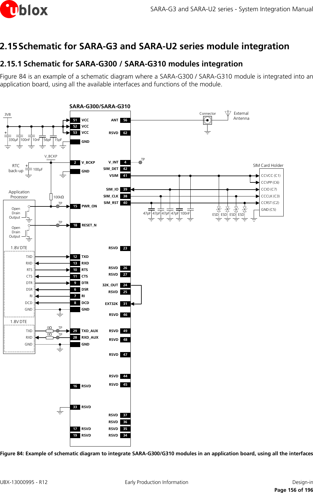
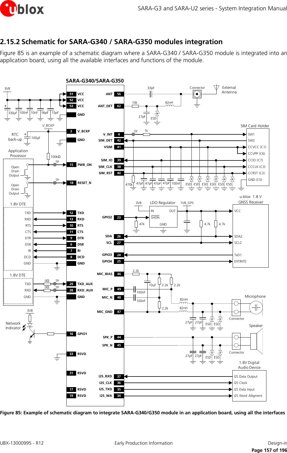
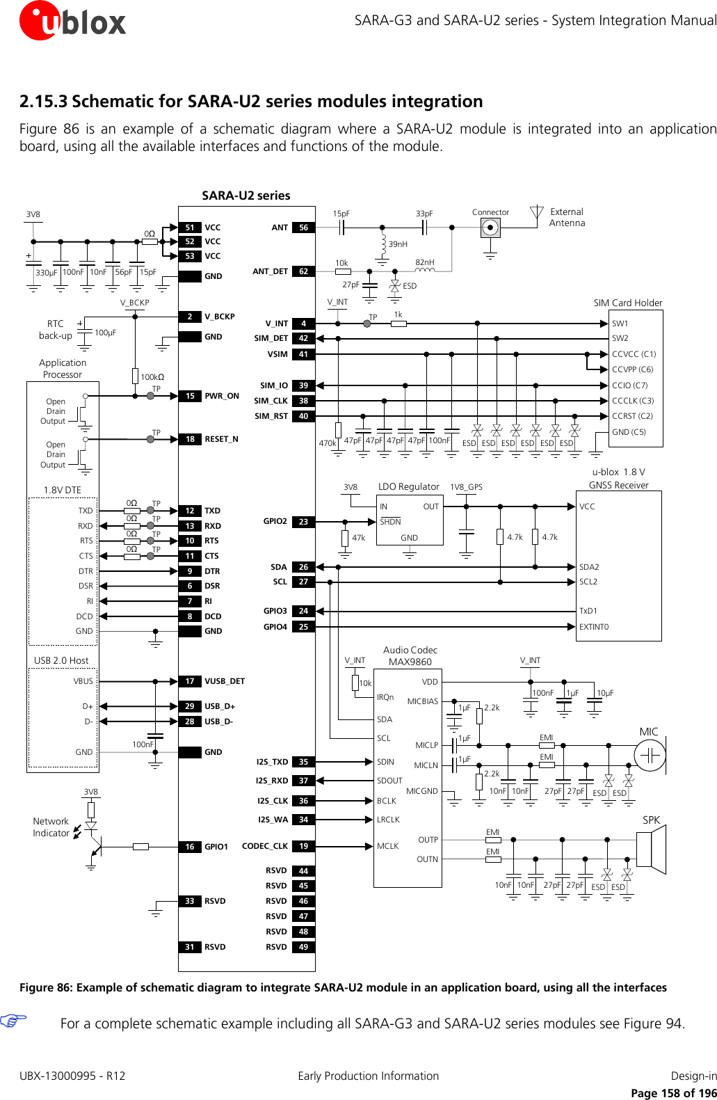
![SARA-G3 and SARA-U2 series - System Integration Manual 2.16 Design-in checklist This section provides a design-in checklist. 2.16.1 Schematic checklist The following are the most important points for a simple schematic check: DC supply must provide a nominal voltage at VCC pin above the minimum operating range limit. DC supply must be capable of providing 1.9 A current pulses, providing a voltage at VCC pin above the minimum operating range limit and with a maximum 400 mV voltage drop from the nominal value. VCC supply should be clean, with very low ripple/noise: provide the suggested bypass capacitors, in particular if the application device integrates an internal antenna. VCC voltage must ramp from 2.5 V to 3.2 V within 4 ms to allow a proper switch-on of the module. Do not leave PWR_ON floating: fix properly the level, e.g. adding a proper pull-up resistor to V_BCKP. Do not apply loads which might exceed the limit for maximum available current from V_INT supply. Check that voltage level of any connected pin does not exceed the relative operating range. Capacitance and series resistance must be limited on each SIM signal to match the SIM specifications. Insert the suggested capacitors on each SIM signal and low capacitance ESD protections if accessible. Check UART signals direction, since the signal names follow the ITU-T V.24 Recommendation [10]. Provide accessible testpoints directly connected to the following pins of the SARA-G3 series modules: TXD_AUX and RXD_AUX pins, V_INT pin, RESET_N and/or PWR_ON pins, for module FW upgrade by the u-blox EasyFlash tool and for diagnostic purpose. Provide accessible testpoints directly connected to the following pins of the SARA-U2 series modules: VUSB_DET, USB_D+, USB_D- and/or RXD, TXD, CTS, RTS pins, V_INT pin, RESET_N and/or PWR_ON pins, for module FW upgrade by the u-blox EasyFlash tool and for diagnostic purpose. Add a proper pull-up resistor (e.g. 4.7 kΩ) to V_INT or another proper 1.8 V supply on each DDC (I2C) interface line, if the interface is used. Capacitance and series resistance must be limited on each high speed line of the USB interface. Capacitance and series resistance must be limited on each line of the DDC (I2C) interface. Use transistors with at least an integrated resistor in the base pin or otherwise put a 10 kΩ resistor on the board in series to the GPIO when those are used to drive LEDs. Connect the pin number 33 (RSVD) to ground. Insert the suggested passive filtering parts on each used analog audio line. Check the digital audio interface specifications to connect a proper device. Capacitance and series resistance must be limited on CODEC_CLK line and each I2S interface line. Provide proper precautions for ESD immunity as required on the application board. Any external signal connected to any generic digital interface pin must be tri-stated or set low when the module is in power-down mode and during the module power-on sequence (at least until the activation of the V_INT output of the module), to avoid latch-up of circuits and let a proper boot of the module. All unused pins can be left unconnected except the PWR_ON pin (its level must be properly fixed, e.g. adding a 100 kΩ pull-up to V_BCKP) and the RSVD pin number 33 (it must be connected to GND). UBX-13000995 - R12 Early Production Information Design-in Page 159 of 196](https://usermanual.wiki/u-blox/SARAU280/User-Guide-2520608-Page-159.png)
![SARA-G3 and SARA-U2 series - System Integration Manual 3 Handling and soldering No natural rubbers, no hygroscopic materials or materials containing asbestos are employed. 3.1 Packaging, shipping, storage and moisture preconditioning For information pertaining to reels and tapes, Moisture Sensitivity levels (MSD), shipment and storage information, as well as drying for preconditioning see the SARA-G3 series Data Sheet [1] or the SARA-U2 series Data Sheet [2] and the u-blox Package Information Guide [27]. 3.2 Handling The SARA-G3 and SARA-U2 series modules are Electro-Static Discharge (ESD) sensitive devices. Ensure ESD precautions are implemented during handling of the module. Electrostatic discharge (ESD) is the sudden and momentary electric current that flows between two objects at different electrical potentials caused by direct contact or induced by an electrostatic field. The term is usually used in the electronics and other industries to describe momentary unwanted currents that may cause damage to electronic equipment. The ESD sensitivity for each pin of SARA-G3 and SARA-U2 series modules (as Human Body Model according to JESD22-A114F) is specified in the SARA-G3 series Data Sheet [1] or the SARA-U2 series Data Sheet [2]. ESD prevention is based on establishing an Electrostatic Protective Area (EPA). The EPA can be a small working station or a large manufacturing area. The main principle of an EPA is that there are no highly charging materials near ESD sensitive electronics, all conductive materials are grounded, workers are grounded, and charge build-up on ESD sensitive electronics is prevented. International standards are used to define typical EPA and can be obtained for example from International Electrotechnical Commission (IEC) or American National Standards Institute (ANSI). In addition to standard ESD safety practices, the following measures should be taken into account whenever handling the SARA-G3 and SARA-U2 series modules: • Unless there is a galvanic coupling between the local GND (i.e. the work table) and the PCB GND, then the first point of contact when handling the PCB must always be between the local GND and PCB GND. • Before mounting an antenna patch, connect ground of the device. • When handling the module, do not come into contact with any charged capacitors and be careful when contacting materials that can develop charges (e.g. patch antenna, coax cable, soldering iron,…). • To prevent electrostatic discharge through the RF pin, do not touch any exposed antenna area. If there is any risk that such exposed antenna area is touched in non ESD protected work area, implement proper ESD protection measures in the design. • When soldering the module and patch antennas to the RF pin, make sure to use an ESD safe soldering iron. For more robust designs, employ additional ESD protection measures on the application device integrating the SARA-G3 and SARA-U2 series modules, as described in section 2.13.3. UBX-13000995 - R12 Early Production Information Handling and soldering Page 161 of 196](https://usermanual.wiki/u-blox/SARAU280/User-Guide-2520608-Page-161.png)
![SARA-G3 and SARA-U2 series - System Integration Manual To avoid falling off, modules should be placed on the topside of the motherboard during soldering. The soldering temperature profile chosen at the factory depends on additional external factors like choice of soldering paste, size, thickness and properties of the base board, etc. Exceeding the maximum soldering temperature and the maximum liquidus time limit in the recommended soldering profile may permanently damage the module. Preheat Heating Cooling[°C] Peak Temp. 245°C [°C]250 250Liquidus Temperature217 217200 20040 - 60 sEnd Temp.max 4°C/s150 - 200°C150 150max 3°C/s60 - 120 s100 Typical Leadfree 100Soldering Profile50 50Elapsed time [s] Figure 87: Recommended soldering profile SARA-G3 and SARA-U2 series modules must not be soldered with a damp heat process. 3.3.3 Optical inspection After soldering the SARA-G3 and SARA-U2 series modules, inspect the modules optically to verify that the module is properly aligned and centered. 3.3.4 Cleaning Cleaning the soldered modules is not recommended. Residues underneath the modules cannot be easily removed with a washing process. • Cleaning with water will lead to capillary effects where water is absorbed in the gap between the baseboard and the module. The combination of residues of soldering flux and encapsulated water leads to short circuits or resistor-like interconnections between neighboring pads. Water will also damage the sticker and the ink-jet printed text. • Cleaning with alcohol or other organic solvents can result in soldering flux residues flooding into the two housings, areas that are not accessible for post-wash inspections. The solvent will also damage the sticker and the ink-jet printed text. • Ultrasonic cleaning will permanently damage the module, in particular the quartz oscillators. For best results use a "no clean" soldering paste and eliminate the cleaning step after the soldering. UBX-13000995 - R12 Early Production Information Handling and soldering Page 163 of 196](https://usermanual.wiki/u-blox/SARAU280/User-Guide-2520608-Page-163.png)
![SARA-G3 and SARA-U2 series - System Integration Manual 4 Approvals For the complete list of all the certification schemes approvals of SARA-G3 and SARA-U2 series modules and the corresponding declarations of conformity, see the u-blox web-site (http://www.u-blox.com). 4.1 Product certification approval overview Product certification approval is the process of certifying that a product has passed all tests and criteria required by specifications, typically called “certification schemes” that can be divided into three distinct categories: • Regulatory certification o Country specific approval required by local government in most regions and countries, as: CE (Conformité Européenne) marking for European Union FCC (Federal Communications Commission) approval for United States • Industry certification o Telecom industry specific approval verifying the interoperability between devices and networks: GCF (Global Certification Forum), partnership between European device manufacturers and network operators to ensure and verify global interoperability between devices and networks PTCRB (PCS Type Certification Review Board), created by United States network operators to ensure and verify interoperability between devices and North America networks • Operator certification o Operator specific approval required by some mobile network operator, as: AT&T network operator in United States Even if the SARA-G3 and SARA-U2 series modules are approved under all major certification schemes, the application device that integrates the modules must be approved under all the certification schemes required by the specific application device to be deployed in the market. The required certification scheme approvals and relative testing specifications differ depending on the country or the region where the device that integrates SARA-G3 and SARA-U2 series modules must be deployed, on the relative vertical market of the device, on type, features and functionalities of the whole application device, and on the network operators where the device must operate. The certification of the application device that integrates a SARA-G3 and SARA-U2 series module and the compliance of the application device with all the applicable certification schemes, directives and standards are the sole responsibility of the application device manufacturer. SARA-G3 and SARA-U2 series modules are certified according to all capabilities and options stated in the Protocol Implementation Conformance Statement document (PICS) of the module. The PICS, according to 3GPP TS 51.010-2 [16] and 3GPP TS 34.121-2 [17], is a statement of the device capabilities and options. The PICS document of the application device integrating a SARA-G3 and SARA-U2 series module must be updated from the module PICS statement if any feature stated as supported by the module in its PICS document is not implemented or disabled in the application device. For more details regarding the AT commands settings that affect the PICS, see the u-blox AT Commands Manual [3]. Check the specific settings required for mobile network operators approvals as they may differ from the AT commands settings defined in the module as integrated in the application device. UBX-13000995 - R12 Early Production Information Approvals Page 165 of 196](https://usermanual.wiki/u-blox/SARAU280/User-Guide-2520608-Page-165.png)
![SARA-G3 and SARA-U2 series - System Integration Manual 4.5 CCC mark SARA-G350 modules are certificated for China compulsory product certification (CCC mark). 4.6 SARA-G350 ATEX and LISA-U270 ATEX conformance for use in explosive atmospheres SARA-G350 ATEX and SARA-U270 ATEX modules are certified as components intended for use in potentially explosive atmospheres compliant to the following standards: • IEC 60079-0: 2011 • IEC 60079-11: 2011 • IEC 60079-26: 2006 The certification numbers of the modules, according to the ATEX directive 94/9/EC, are: • SIQ 13 ATEX 032 U for SARA-G350 ATEX • SIQ TBD for SARA-U270 ATEX The certification numbers of the modules, according to the IECEx conformity assessment system, are: • IECEx SIQ 13.0004U for SARA-G350 ATEX • IECEx SIQ TBD for LISA-U270 ATEX According to the standards listed above, SARA-G350 ATEX and LISA-U270 ATEX modules are certified with the following marking: • Ex II 1G, Ex ia IIC/IIB The temperature range for using SARA-G350 ATEX and SARA-U270 ATEX modules is defined in the ‘Operating temperature range’ section of the SARA-G3 series Data Sheet [1] and SARA-U2 series Data Sheet [2] respectively. The RF radiating profile of SARA-G350 ATEX and SARA-U270 ATEX modules is compliant to all the applicable 3GPP / ETSI standards, with a maximum of 2 W RF pulse power and 1.15 mJ RF pulse energy according to the GSM/GPRS power class stated in Table 2; the maximum average power of SARA-U270 ATEX, according to the WCDMA power class stated in Table 3, is 250 mW. The nameplate of SARA-G350 ATEX and SARA-U270 modules is described in the ‘Product labeling’ section of the SARA-G3 series Data Sheet [1] and SARA-U2 series Data Sheet [2]. Table 61 lists the maximum input and equivalent parameters that must be considered in sub-division IIC for SARA-G350 ATEX and SARA-U270 ATEX. Parameter SARA-G350 ATEX SARA-U270 ATEX Ui 3.8 V 3.8 V Ii 1.6 A (burst) 1.6 A (burst) Pi 2.5 W TBD W Ci 103 µF 132 µF Li 4.1 µH 9.8 µH Table 61: Maximum input and equivalent parameters for sub-division IIC UBX-13000995 - R12 Early Production Information Approvals Page 170 of 196](https://usermanual.wiki/u-blox/SARAU280/User-Guide-2520608-Page-170.png)
![SARA-G3 and SARA-U2 series - System Integration Manual • Component assembly on the device; it should be verified that: o Communication with host controller can be established o The interfaces between module and device are working o Overall RF performance test of the device including antenna Dedicated tests can be implemented to check the device. For example, the measurement of module current consumption when set in a specified status can detect a short circuit if compared with a “Golden Device” result. Module AT commands are used to perform functional tests (communication with host controller, check SIM card interface, check communication between module and GNSS, GPIOs, etc.) and to perform RF performance tests. 5.2.1 “Go/No go” tests for integrated devices A ‘Go/No go’ test is to compare the signal quality with a “Golden Device” in a position with excellent network coverage and after having dialed a call (see u-blox AT Commands Manual [3], AT+CSQ command: <rssi>, <ber> parameters). These kinds of test may be useful as a ‘go/no go’ test but not for RF performance measurements. This test is suitable to check the communication with host controller and SIM card, the audio and power supply functionality and verify if components at antenna interface are well soldered. 5.2.2 Functional tests providing RF operation Overall RF performance test of the device including antenna can be performed with basic instruments such as a spectrum analyzer (or an RF power meter) and a signal generator using AT+UTEST command over AT interface. The AT+UTEST command gives a simple interface to set the module to Rx and Tx test modes ignoring 2G/3G signaling protocol. The command can set the module: • In transmitting mode in a specified channel and power level in all the supported modulation schemes (single slot GMSK, single slot 8PSK, WCDMA) and bands 2G, 3G • In receiving mode in a specified channel to returns the measured power level in all 2G/3G supported bands See the u-blox AT Commands Manual [3], for AT+UTEST command syntax description. See the End user test Application Note [26], for AT+UTEST command user guide, limitations and examples of use. UBX-13000995 - R12 Early Production Information Product testing Page 173 of 196](https://usermanual.wiki/u-blox/SARAU280/User-Guide-2520608-Page-173.png)
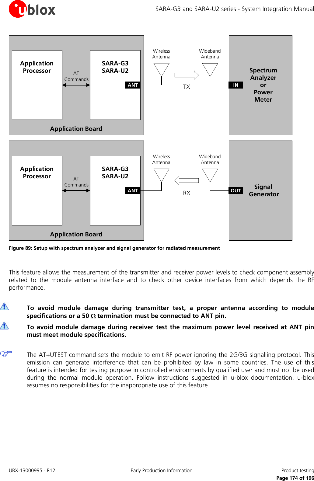
![SARA-G3 and SARA-U2 series - System Integration Manual The voltage level of all the digital interfaces of SARA and LISA modules is 1.8 V: this allows the direct connection from a 1.8 V external device (e.g. application processor) to all the modules. The following sections explain in detail all the points to consider during the migration between LISA and SARA designs, implementing or not a nested design For further details regarding SARA-G3 and LISA characteristics, usage, or settings, see the related module datasheet [1], [4], [5], [6], System Integration Manual [7], [8], and AT commands manual [3], [9]. A.2 Checklist for migration Have you chosen the optimal SARA-G3 module? For quad-band GSM/GPRS, full feature set, select the SARA-G350 module. For dual-band GSM/GPRS, full feature set, select the SARA-G340 module. For quad-band GSM/GPRS, reduced feature set, select the SARA-G310 module. For dual-band GSM/GPRS, reduced feature set, select the SARA-G300 module. Check SARA-G3 modules hardware requirements Check power capabilities of the external supply circuit: SARA-G3 modules require large current pulses in connected-mode as well as LISA-U series modules when a 2G call is enabled. LISA-C2 series modules do not require large current pulses due to the CDMA channel access technology. Check supported bands for proper antenna circuit development: SARA-G3 modules frequency ranges are within LISA-U modules ranges, but LISA-C2 modules range is quite different. Check antenna detection requirements: SARA-G340 and SARA-G350 modules provide the antenna detection function implementing an external application circuit between ANT_DET and ANT pins. Check the module power-on requirements: Table 63 and relative section summarize differences between SARA-G3 and LISA modules. Check the module requirements to enter low power idle-mode: SARA-G300 and SARA-G310 modules require a 32 kHz signal at EXT32K input, which for example can be provided by the 32K_OUT output. Check serial interfaces requirements: SARA-G3 modules provide UART interface for AT command, data communication, multiplexer functionality, FW upgrade over AT and provide auxiliary UART interface for FW upgrade using the u-blox EasyFlash tool and for diagnostic purpose. Check analog audio requirements: SARA-G340 and SARA-G350 modules do not provide DC blocking capacitors at the MIC_P / MIC_N input pins and provide supply output and local ground for an external microphone at the MIC_BIAS / MIC_GND pins. Check digital audio requirements: SARA-G340 and SARA-G350 modules provide a 4-wire 1.8 V interface supporting PCM and Normal I2S modes, master role and fixed sample rate. Check internal active pull-up / down values at digital interface input pins and the current capability of digital interface output pins, since they are slightly different between SARA-G3 and LISA modules. Check SARA-G3 modules software requirements Not all of the functionalities available with LISA modules are supported by all the SARA-G3 modules versions. SARA-G300 and SARA-G310 modules do not support: o Audio interfaces, DDC (I2C) interface, Antenna detection interface, GPIOs o Low power idle-mode, if a 32 kHz signal at EXT32K input pin is not provided o TCP/IP, UDP/IP, FTP, HTTP o GNSS via Modem, AssistNow clients, Hybrid positioning and CellLocate® functionalities o Jamming detection UBX-13000995 - R12 Early Production Information Appendix Page 177 of 196](https://usermanual.wiki/u-blox/SARAU280/User-Guide-2520608-Page-177.png)
![SARA-G3 and SARA-U2 series - System Integration Manual A.3 Software migration Software migration between SARA-G3 and LISA cellular modules is a straightforward procedure. Nevertheless there are some differences to be considered with firmware version. Each cellular module supports AT commands according to 3GPP standards: TS 27.007 [11], TS 27.005 [12], TS 27.010 [13] and the u-blox AT command extension. Backward compatibility has been maintained as far as possible. For the complete list of supported AT commands and their syntax see the relevant AT commands manual of the module [3], [9]. A.4 Hardware migration SARA modules have been designed with backward compatibility to LISA series modules in mind but some minor differences were unavoidable. These minor differences are however not relevant for the majority of the designs. The following subsections describe the hardware differences between the interfaces of SARA-G3 modules and LISA modules while Table 64 summarizes the detailed differences between the pins. A.4.1 Supply interfaces Module supply input (VCC) The same compatible external circuit can be implemented for SARA and LISA modules even if there are minor differences in the VCC input voltage ranges and some differences in the current consumption figures. The voltage provided must be within the normal operating range limits to allow module switch-on and must be above the minimum limit of the extended operating range to avoid module switch-off. For the detailed VCC input voltage ranges values see Table 64 or to the relative datasheet of the module [1], [4], [5], [6]. The SARA-G3 maximum average current consumption is lower than the LISA one due to the lower data rate or the different channel access technology. SARA-G3 modules require large current pulses in connected-mode as well as LISA-U series when a 2G call is enabled. LISA-C2 series do not require large current pulses due to the CDMA channel access technology. For the detailed current consumption values see the related module datasheet [1], [4], [5], [6]. Detailed supply circuit design-in guidelines are reported in section 2.2.1 and in the corresponding System Integration Manual of the module [7], [8]. RTC supply input/output (V_BCKP) The same compatible external circuit can be implemented for SARA and LISA-U series even if there are minor differences in the V_BCKP typical output voltage and input voltage range as reported in Table 64 or in the relative datasheet of the module [1], [4], [5], [6]. LISA-C2 series do not provide V_BCKP RTC supply input/output as well as the whole RTC functionality. Interfaces supply output (V_INT) The same compatible external circuit can be implemented for SARA and LISA series: there are no differences in the V_INT output characteristics. UBX-13000995 - R12 Early Production Information Appendix Page 178 of 196](https://usermanual.wiki/u-blox/SARAU280/User-Guide-2520608-Page-178.png)
![SARA-G3 and SARA-U2 series - System Integration Manual A.4.2 System functions interfaces Module power-on SARA-G3 and LISA series power-on sequence is initiated in one of the ways summarized in Table 63. For more details, see section 1.6.1 or to the relative System Integration Manual of the module [7], [8]. SARA-G3 series LISA-C2 series LISA-U1 series LISA-U2 series Rising edge on the VCC pins to a valid voltage as module supply Rising edge on the VCC pins to a valid voltage as module supply with PWR_ON pin permanently low when VCC is applied Rising edge on the VCC pins to a valid voltage as module supply Rising edge on the VCC pins to a valid voltage as module supply Low level on the PWR_ON pin for appropriate time period Low pulse on the PWR_ON pin for appropriate time period Low pulse on the PWR_ON pin for appropriate time period Low pulse on the PWR_ON pin for appropriate time period Pre-programmed RTC alarm (not supported by SARA-G300/G310) Pre-programmed RTC alarm Pre-programmed RTC alarm RESET_N input pin released from the low level RESET_N input pin released from the low level Table 63: Summary of power on events among modules The same compatible external power-on circuit can be implemented for SARA and LISA modules even if there are minor differences in the PWR_ON input voltage levels ranges and in the low level time or low pulse time to switch-on the module, as reported in Table 64 or in the relative datasheet of the module [1], [4], [5], [6]. PWR_ON falling edge (i.e. low pulse) is required for LISA series, but it is not required for SARA. External pull-up is not needed for LISA-C2 series since internal pull-up is provided. Module power-off SARA and LISA modules can all be properly switched off by means of the AT+CPWROFF command. Additionally, all LISA-U2 modules, except LISA-U200-00S, can be properly switched off by low pulse on the PWR_ON pin, as reported in Table 64 or in the relative datasheet of the module [6]. Module reset SARA and LISA modules reset can be performed in one of the following ways: • Forcing a low level on the RESET_N pin, causing an “external” or “hardware” reset • By means of the AT+CFUN command, causing an “internal” or “software” reset The same compatible external reset circuit can be implemented for SARA and LISA modules even if there are minor differences in the RESET_N input voltage levels ranges and in the low level time, as reported in Table 64 or in the relative datasheet of the module [1], [4], [5], [6]. Additional precautions are suggested for the RESET_N line of LISA-U series modules, depending on the application board handling, to satisfy ESD immunity test requirements as described in the LISA-U Series System Integration Manual [8]. External 32 kHz input and internal 32 kHz output The EXT32K input and the 32K_OUT output are available only on the SARA-G300 and SARA-G310 modules to provide the 32 kHz reference clock for the Real Time Clock (RTC) timing, used by the module processor to reach the low power idle-mode and provide the RTC functions. SARA-G340, SARA-G350 and LISA-U modules are equipped with internal 32 kHz oscillator to provide the same functions. LISA-C2 series do not provide RTC and the relative functions. UBX-13000995 - R12 Early Production Information Appendix Page 179 of 196](https://usermanual.wiki/u-blox/SARAU280/User-Guide-2520608-Page-179.png)
![SARA-G3 and SARA-U2 series - System Integration Manual A.4.3 Antenna interface RF interface for Tx/Rx antenna The same compatible external circuit can be implemented for SARA and LISA series ANT pin even if there are some differences in the operating bands frequency ranges, as summarized in Figure 92. VV II II850900850800 850 900 950900 18001900 190018001700 1750 1800 1850 1900 1950 2000 2050 2100 2150 2200824 960 1710 1990LISA-U100 LISA-U120 LISA-U260LISA-U200 LISA-U230VV II II850900850800 850 900 950900 18001900 190018001700 1750 1800 1850 1900 1950 2000 2050 2100 2150 2200IIVIVIVIIIVIII IV IV824 960 1710 2170850900850800 850 900 950900 18001900 190018001700 1750 1800 1850 1900 1950 2000 2050 2100 2150 2200IIVIIIVIII824 960 1710 2170LISA-U110 LISA-U130 LISA-U270850900850800 850 900 950900 18001900 190018001700 1750 1800 1850 1900 1950 2000 2050 2100 2150 2200824 960 1710 1990SARA-G310 SARA-G350900800 850 900 950900 1800 18001700 1750 1800 1850 1900 1950 2000 2050 2100 2150 2200880 960 1710 1880SARA-G300SARA-G340800800800 850 900 9501900 19001700 1750 1800 1850 1900 1950 2000 2050 2100 2150 2200824 894 1850 1990LISA-C200 Figure 92: Summary of operating bands frequency ranges among modules An external circuit can be implemented on the application device integrating SARA-U2 and LISA-U2 modules to satisfy ESD immunity test requirements at the antenna port, as described in sections 2.13 and 2.4, and in the LISA-U Series System Integration Manual [8]. The same external circuit is not required for SARA-G3, LISA-U1 and LISA-C2 modules. RF interface for Rx diversity antenna Only the LISA-U230 modules provide the RF input for Rx diversity antenna (ANT_DIV). SARA-G3, LISA-C2, LISA-U1 and the other LISA-U2 series modules do not support Rx diversity. Antenna detection interface An external application circuit can be implemented on the application device integrating SARA-G340 / SARA-G350 modules to provide antenna detection functionality, with a proper connection between the ANT_DET pin and the ANT pin, as described in section 2.4.2. LISA-U modules are equipped with internal circuit for antenna detection support. SARA-G300, SARA-G310 and LISA-C2 series modules do not support antenna detection. UBX-13000995 - R12 Early Production Information Appendix Page 180 of 196](https://usermanual.wiki/u-blox/SARAU280/User-Guide-2520608-Page-180.png)
![SARA-G3 and SARA-U2 series - System Integration Manual A.4.4 SIM interface SIM interface The same compatible external circuit can be implemented for SARA and LISA modules: 1.8 V and 3.0 V SIM are supported. LISA-C2 modules do not need an external SIM for Sprint and Verizon mobile operators. LISA-C2 series SIM interface is hardware ready but the support of external SIM card / IC will be provided by the upcoming firmware releases. SIM detection interface The same compatible external circuit can be implemented for SARA and LISA modules: SIM detection function is provided by the SIM_DET pin on SARA-G3 modules and by the GPIO5 pin on LISA-U modules. SIM card hot insertion/removal is additionally supported by all LISA-U2 series except LISA-U200-00S. LISA-C2 modules do not support SIM detection. A.4.5 Serial interfaces UART interface The same compatible external circuit can be implemented for SARA and LISA modules: a 1.8 V unbalanced asynchronous serial port with RS-232 functionality is provided on SARA-G3 modules (for AT command, data communication, MUX functionality, FW upgrade over AT), LISA-C2 modules (for AT command, data communication, MUX functionality), LISA-U modules (for AT command, data communication, MUX functionality, FW upgrade over AT or using the u-blox EasyFlash tool). LISA-C2 modules do not support DSR, DCD and DTR functions. Table 64 and the module’s datasheet [1], [4], [5], [6] report minor differences in the internal pull-ups and drivers strengths. These are the default settings of the UART interfaces: • SARA-G3 modules: automatic baud rate and frame format detection • LISA-U2 except LISA-U200-00S modules: one-shot automatic baud rate and frame format detection • LISA-C2, LISA-U1 and LISA-U200-00S modules: 115200 b/s baud rate and 8N1 frame format For further details regarding UART interface settings see the module’s datasheet [1], [4], [5], [6] and to the related AT commands manual of the module [3], [9]. UART AUX interface Only the SARA-G3 modules provide an auxiliary UART interface for FW upgrade using the u-blox EasyFlash tool and for diagnostic purpose. LISA modules do not provide an auxiliary UART interface. USB interface SARA-G3 modules do not provide a USB interface such as is available on LISA-U modules (High-Speed USB 2.0 for AT command, data communication, FW upgrade over AT or using the u-blox EasyFlash tool, and for Trace log capture) and on LISA-C2 modules (Full-Speed USB 2.0 for AT command, Data communication, FW upgrade). SPI interface SARA-G3 and LISA-C2 modules do not provide an SPI interface such as is available on LISA-U modules (5-wire IPC interface for AT command, data communication, MUX functionality, FW upgrade over AT). DDC (I2C) interface The same compatible external circuit can be implemented for SARA-G340 / SARA-G350 and LISA series: A 1.8 V DDC (I2C bus compatible) interface is provided to communicate with u-blox GNSS receivers. UBX-13000995 - R12 Early Production Information Appendix Page 181 of 196](https://usermanual.wiki/u-blox/SARAU280/User-Guide-2520608-Page-181.png)
![SARA-G3 and SARA-U2 series - System Integration Manual SARA-G300, SARA-G310 and LISA-U200-00S modules do not support the DDC (I2C) interface. LISA-C2 modules will support the DDC (I2C) interface in the upcoming firmware releases. All LISA-U2 modules, except LISA-U200-00S, additionally support the communication with I2C slaves by means of dedicated AT commands, other than u-blox positioning receivers over the same DDC (I2C) interface. A.4.6 Audio interfaces Analog audio interfaces Differential analog audio input is provided on the MIC_P / MIC_N pins of SARA-G340 / SARA-G350 modules (without internal DC blocking capacitor) and LISA-C2 series, LISA-U120, and LISA-U130 modules (with an internal DC blocking capacitor). Supply output and local ground for an external microphone is provided on the MIC_BIAS / MIC_GND pins of SARA-G340 / SARA-G350 modules only: the supply for an external microphone has to be provided by an external LDO linear regulator with the other modules. Differential analog audio output is provided on the SPK_P / SPK_N pins of SARA-G340, SARA-G350, LISA-U120, LISA-U130 modules (16 ohm load capable) and LISA-C2 series modules (32 ohm load capable). SARA-G300/SARA-G310, LISA-U100/U110, LISA-U200-00S modules do not provide analog audio interfaces. LISA-U2 series modules do not provide analog audio interfaces, but analog audio can be provided with external audio codec connected to a digital audio interface of all LISA-U2 series modules except LISA-U200-00S (e.g. the 4-wire I2S digital audio interface provided instead of the 4 analog audio pins). The modules provide control of the external codec by means of the I2C interface and clock reference by means of the CODEC_CLK pin. For further details regarding analog audio interfaces characteristics, usage, and settings, see the related module datasheet [1], [4], [5], [6], System Integration Manual 1.10.1, 2.7.1, [7], [8], and AT commands manual [3], [9]. Digital audio interfaces The digital audio interface is provided on the I2S_TXD, I2S_RXD, I2S_CLK, I2S_WA pins of SARA-G340 / SARA-G350 modules (1.8 V, PCM & Normal I2S modes, master, fixed sample rate) and LISA-U120/U130 and all LISA-U2 series modules except LISA-U200-00S (1.8 V, PCM & Normal I2S modes, master & slave, configurable sample rate). It is provided on the PCM_DO, PCM_DI, PCM_CLK, PCM_SYNC pins of LISA-C2 series modules (1.8 V, PCM). The same compatible external circuit can be implemented according to external digital audio device capabilities. An additional digital audio interface is provided on I2S1_TXD, I2S1_RXD, I2S1_CLK, I2S1_WA pins of all LISA-U2 series except LISA-U200-00S (1.8 V, PCM & Normal I2S modes, master & slave, configurable sample rate). SARA-G300/SARA-G310, LISA-U100/LISA-U110, LISA-U200-00S modules do not provide digital audio interfaces. For further details regarding digital audio interfaces characteristics, usage, and settings, see the related module datasheet [1], [4], [5], [6], System Integration Manual 1.10.2, 2.7.2, [7], [8], and AT commands manual [3], [9]. A.4.7 GPIO pins The same compatible external circuit can be implemented for SARA-G340 / SARA-G350 and LISA series: four 1.8 V GPIOs are provided by SARA-G340 / SARA-G350 modules, providing the same functionalities as LISA series modules except Module Status and Operating Mode Indications. The SIM_DET pin provides the SIM detection function on SARA modules rather than the GPIO5 pin as on LISA-U series modules. SARA-G300 and SARA-G310 modules do not provide GPIOs. A.4.8 Reserved pins SARA modules RSVD pin 33 must be connected to ground, as does the RSVD pin 5 on LISA modules. UBX-13000995 - R12 Early Production Information Appendix Page 182 of 196](https://usermanual.wiki/u-blox/SARAU280/User-Guide-2520608-Page-182.png)
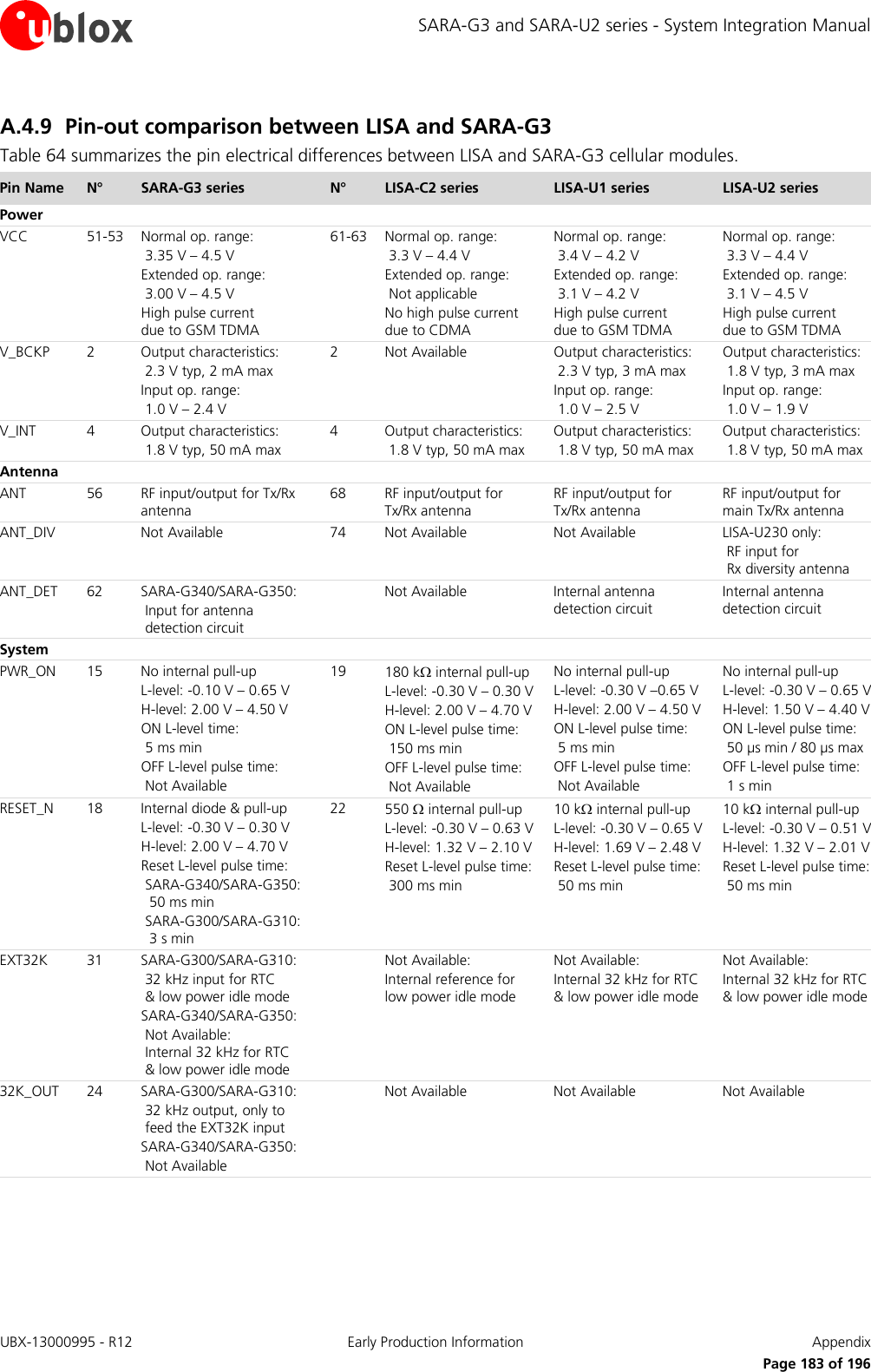
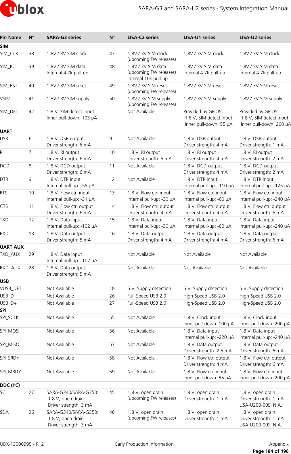
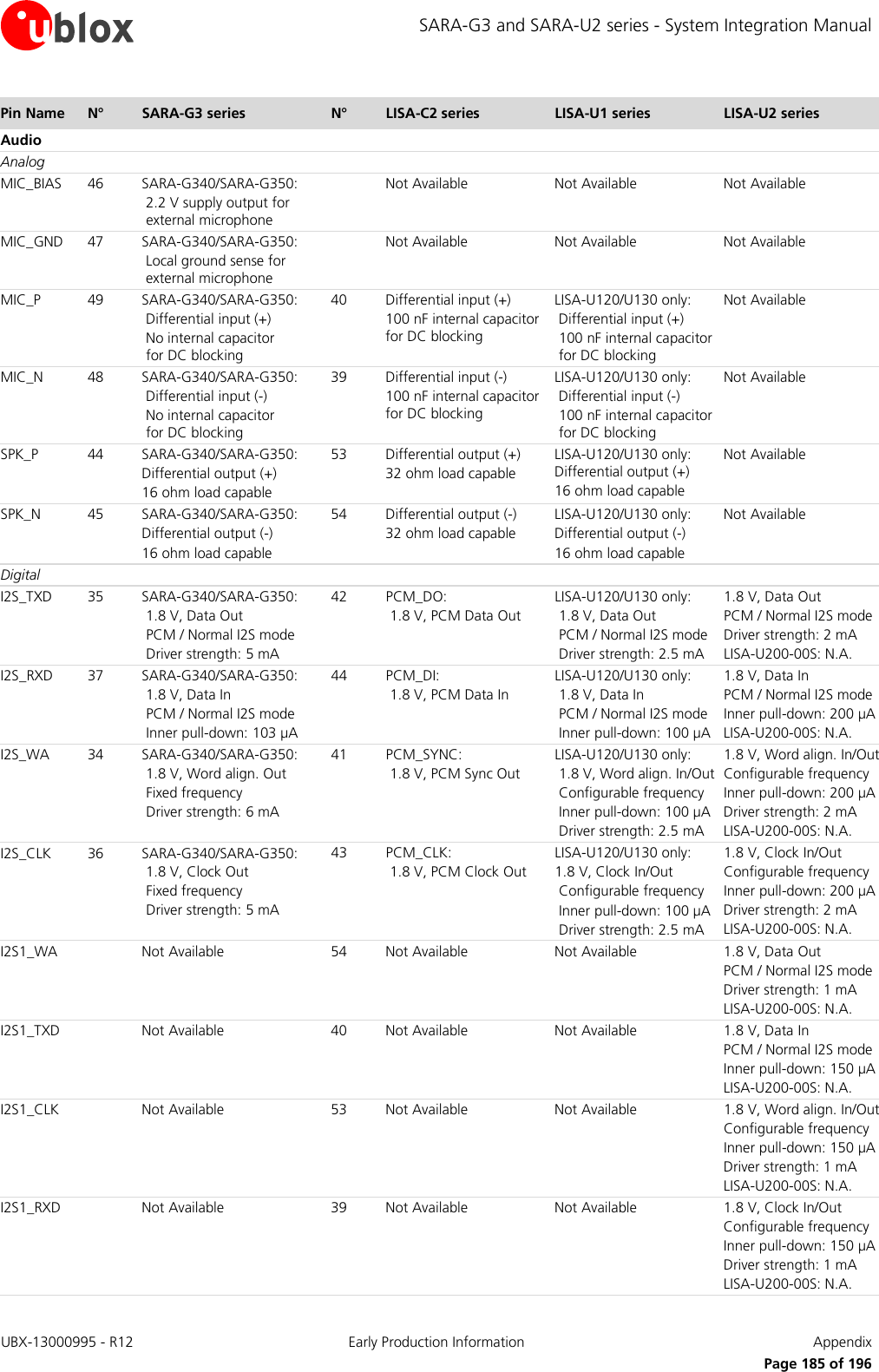
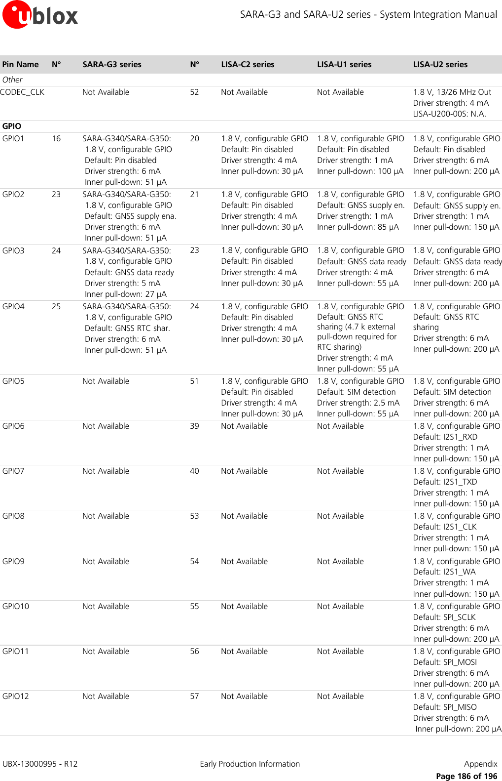
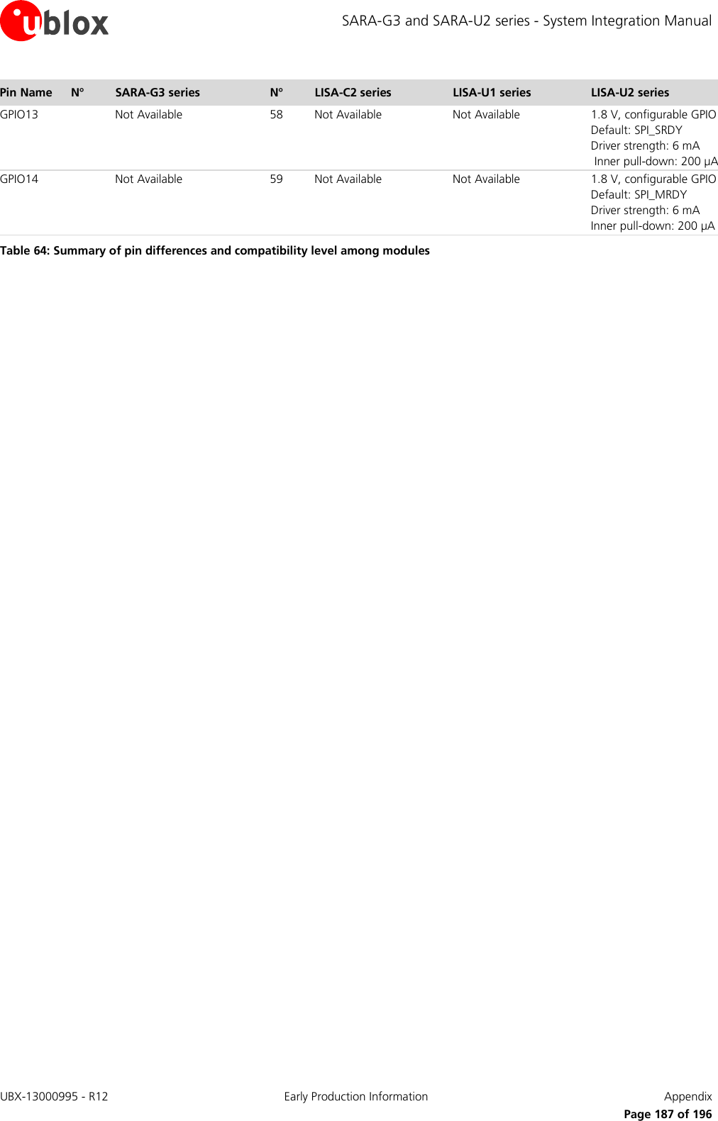
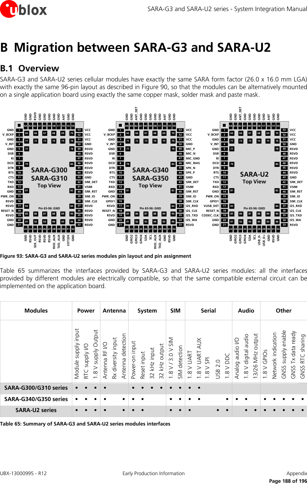
![SARA-G3 and SARA-U2 series - System Integration Manual SARA-G3 SARA-U2 Pin No Pin Name Description Pin Name Description Remarks for migration 25 GPIO4 / RSVD 1.8 V GPIO / Reserved Default: GNSS RTC sharing Driver strength: 6 mA Internal pull-down: ~35 k GPIO4 1.8 V GPIO Default: GNSS RTC sharing Driver strength: 6 mA Internal pull-down: ~9 k No functional difference 26 SDA / RSVD I2C Data I/O / Reserved 1.8 V, open drain Driver strength: 3 mA SDA I2C Data I/O 1.8 V, open drain Driver strength: 1 mA No functional difference 27 SCL / RSVD I2C Clock Output / Reserved 1.8 V, open drain Driver strength: 3 mA SCL I2C Clock Output 1.8 V, open drain Driver strength: 1 mA No functional difference 28 RXD_AUX Aux UART Data Out 1.8 V, Driver strength: 5 mA USB_D- USB Data I/O (D-) High-Speed USB 2.0 USB instead of Auxiliary UART 29 TXD_AUX Aux UART Data In 1.8 V, Internal pull-up:~18 k USB_D+ USB Data I/O (D+) High-Speed USB 2.0 USB instead of Auxiliary UART 30 GND Ground GND Ground 31 RSVD / EXT32K Reserved / 32 kHz Input RSVD Reserved No functional difference 32 GND Ground GND Ground 33 RSVD Reserved RSVD Reserved No functional difference 34 I2S_WA / RSVD I2S Word Alignment / Reserved 1.8 V, Driver strength: 6 mA I2S_WA I2S Word Alignment 1.8 V, Driver strength: 2 mA No functional difference 35 I2S_TXD / RSVD I2S Data Output / Reserved 1.8 V, Driver strength: 5 mA I2S_TXD I2S Data Output 1.8 V, Driver strength: 2 mA No functional difference 36 I2S_CLK / RSVD I2S Clock / Reserved 1.8 V, Driver strength: 5 mA I2S_CLK I2S Clock 1.8 V, Driver strength: 2 mA No functional difference 37 I2S_RXD / RSVD I2S Data Input / Reserved 1.8 V, Internal pull-down:~18 k I2S_RXD I2S Data Input 1.8 V, Inner pull-down: ~9 k No functional difference 38 SIM_CLK SIM Clock Output SIM_CLK SIM Clock Output No functional difference 39 SIM_IO SIM Data I/O SIM_IO SIM Data I/O No functional difference 40 SIM_RST SIM Reset Output SIM_RST SIM Reset Output No functional difference 41 VSIM SIM Supply Output VSIM SIM Supply Output No functional difference 42 SIM_DET SIM Detection Input 1.8 V, Internal pull-down:~18 k SIM_DET SIM Detection Input 1.8 V, Inner pull-down: ~9 k No functional difference 43 GND Ground GND Ground 44 SPK_P / RSVD Analog Audio Out (+) / Reserved RSVD Reserved Analog audio not supported 45 SPK_N / RSVD Analog Audio Out (-) / Reserved RSVD Reserved Analog audio not supported 46 MIC_BIAS / RSVD Microphone Supply Out / Reserved RSVD Reserved Analog audio not supported 47 MIC_GND / RSVD Microphone Ground / Reserved RSVD Reserved Analog audio not supported 48 MIC_N / RSVD Analog Audio In (-) / Reserved RSVD Reserved Analog audio not supported 49 MIC_P / RSVD Analog Audio In (+) / Reserved RSVD Reserved Analog audio not supported 50 GND Ground GND Ground 51-53 VCC Module Supply Input Normal op. range: 3.35 V – 4.5 V Extended op. range: 3.00 V – 4.5 V VCC Module Supply Input Normal op. range: 3.3 V – 4.4 V Extended op. range: 3.1 V – 4.5 V No functional difference 54-55 GND Ground GND Ground 56 ANT RF Antenna I/O ESD immunity (IEC 61000-4-2): ±4 kV contact / ±8 kV air ESD ANT RF Antenna I/O ESD immunity (IEC 61000-4-2): ±2 kV contact / ±4 kV air ESD No functional difference 57-61 GND Ground GND Ground 62 ANT_DET / RSVD Antenna Detection Input / Reserved ANT_DET Antenna Detection Input No functional difference 63-96 GND Ground GND Ground Table 66: SARA-G3 and SARA-U2 pin assignment with remarks for migration For the detailed functional description of each interface of SARA-G3 and SARA-U2 series modules see the related section in the section 1, whereas for detailed design-in see the related section in the chapter 2. For the detailed electrical characteristics of each interface of SARA-G3 and SARA-U2 series modules see the SARA-G3 series Data Sheet [1] and the SARA-U2 series Data Sheet [2]. UBX-13000995 - R12 Early Production Information Appendix Page 190 of 196](https://usermanual.wiki/u-blox/SARAU280/User-Guide-2520608-Page-190.png)
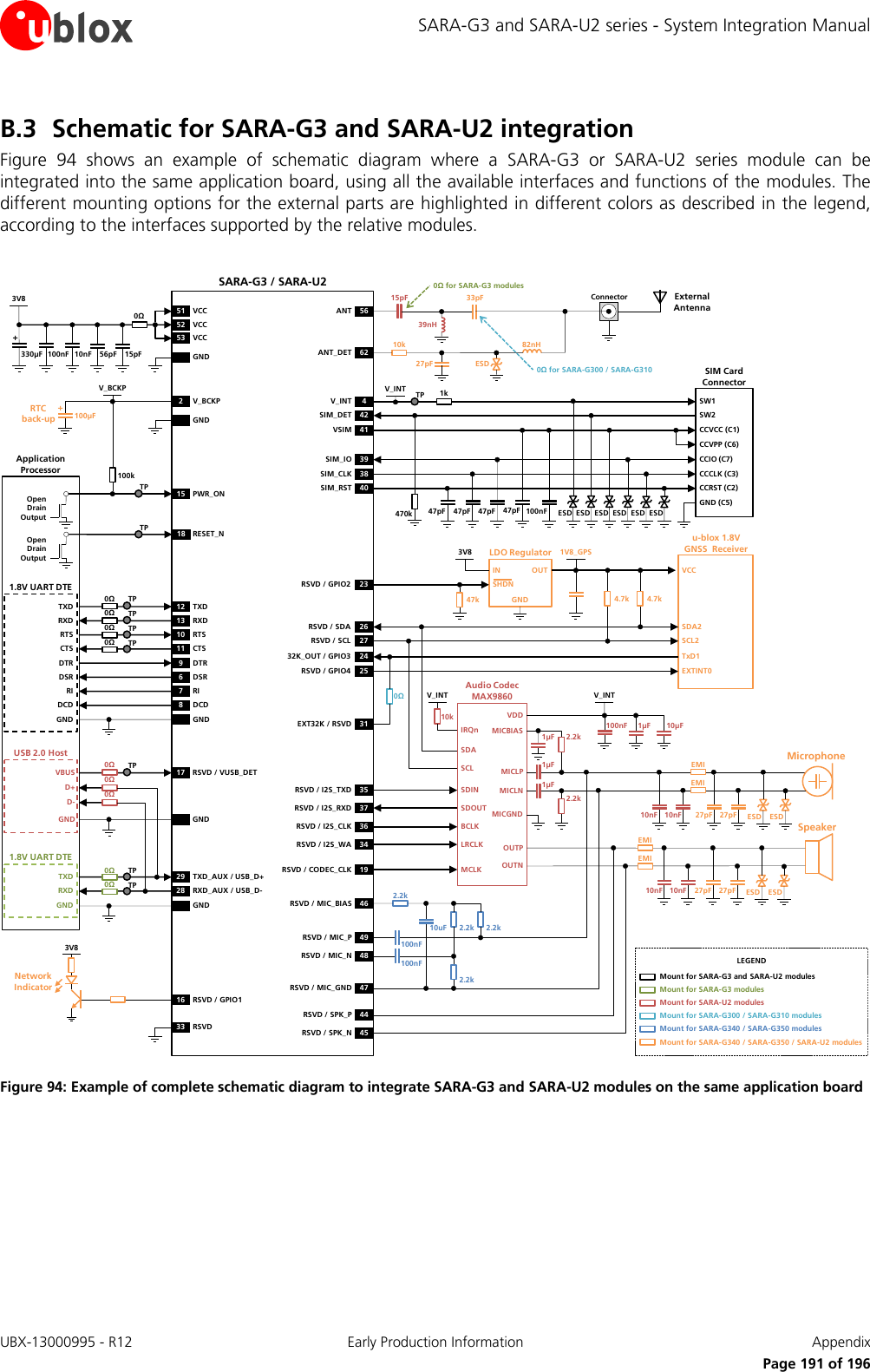
![SARA-G3 and SARA-U2 series - System Integration Manual Related documents [1] u-blox SARA-G3 series Data Sheet, Docu No UBX-13000993 [2] u-blox SARA-U2 series Data Sheet, Docu No UBX-13005287 [3] u-blox AT Commands Manual, Docu No UBX-13002752 [4] u-blox LISA-C200 series Data Sheet, Docu No UBX-13000623 [5] u-blox LISA-U1 series Data Sheet, Docu No UBX-13002048 [6] u-blox LISA-U2 series Data Sheet, Docu No UBX-13001734 [7] u-blox LISA-C200 & FW75-C200/D200 System Integration Manual, Docu No UBX-13000620 [8] u-blox LISA-U series System Integration Manual, Docu No UBX-13001118 [9] u-blox C200 AT Commands Manual, Docu No UBX-13000621 [10] ITU-T Recommendation V.24 - 02-2000 - List of definitions for interchange circuits between the Data Terminal Equipment (DTE) and the Data Circuit-terminating Equipment (DCE). http://www.itu.int/rec/T-REC-V.24-200002-I/en [11] 3GPP TS 27.007 – AT command set for User Equipment (UE) (Release 1999) [12] 3GPP TS 27.005 – Use of Data Terminal Equipment – Data Circuit terminating; Equipment (DTE – DCE) interface for Short Message Service (SMS) and Cell Broadcast Service (CBS) (Release 1999) [13] 3GPP TS 27.010 – Terminal Equipment to User Equipment (TE-UE) multiplexer protocol (Release 1999) [14] Universal Serial Bus Revision 2.0 specification, http://www.usb.org/developers/docs/usb20_docs/ [15] I2C-bus specification and user manual - Rev. 5 - 9 October 2012 - NXP Semiconductors, http://www.nxp.com/documents/user_manual/UM10204.pdf [16] 3GPP TS 51.010-2 – Technical Specification Group GSM/EDGE Radio Access Network; Mobile Station (MS) conformance specification; Part 2: Protocol Implementation Conformance Statement (PICS) [17] 3GPP TS 34.121-2 – Technical Specification Group Radio Access Network; User Equipment (UE) conformance specification; Radio transmission and reception (FDD); Part 2: Implementation Conformance Statement (ICS) [18] CENELEC EN 61000-4-2 (2001) – Electromagnetic compatibility (EMC); Part 4-2: Testing and measurement techniques; Electrostatic discharge immunity test [19] ETSI EN 301 489-1 V1.8.1 – Electromagnetic compatibility and Radio spectrum Matters; EMC standard for radio equipment and services; Part 1: Common technical requirements [20] ETSI EN 301 489-7 V1.3.1 – Electromagnetic compatibility and Radio spectrum Matters; EMC standard for radio equipment and services; Part 7: Specific conditions for mobile and portable radio and ancillary equipment of digital cellular radio telecommunications systems (GSM and DCS) [21] ETSI EN 301 489-24 V1.4.1 – Electromagnetic compatibility and Radio spectrum Matters; EMC standard for radio equipment and services; Part 24: Specific conditions for IMT-2000 CDMA Direct Spread (UTRA) for Mobile and portable (UE) radio and ancillary equipment [22] 3GPP TS 26.267 V10.0.0 – eCall Data Transfer; In-band modem solution; General description (Rel. 10) [23] u-blox Multiplexer Implementation Application Note, Docu No UBX-13001887 [24] u-blox GNSS Implementation Application Note, Docu No UBX-13001849 [25] u-blox Firmware Update Application Note, Docu No UBX-13001845 [26] u-blox End user test Application Note, Docu No UBX-13001922 [27] u-blox Package Information Guide, Docu No UBX-14001652 [28] SIM Access Profile Interoperability Specification, Revision V11r00, http://www.bluetooth.org [29] u-blox eCall / ERA-GLONASS Application Note, Docu No UBX-13001924 [30] BS EN 16062:2011 – Intelligent transport systems – eSafety – eCall high level application requirements [31] ETSI TS 122 101 V8.7.0 – Service aspects; Service principles (3GPP TS 22.101 v.8.7.0 Rel. 8) [32] IEC 60079-0 - Explosive atmospheres, Part 0: Equipment general requirements - 2011-06 [33] IEC 60079-11 - Explosive atmospheres, Part 11: Equipment protection by intrinsic safety 'i' - 2011-06 [34] IEC 60079-26 - Explosive atmospheres, Part 26: Equipment with EPL Ga - 2006-08 Some of the above documents can be downloaded from u-blox web-site (http://www.u-blox.com). UBX-13000995 - R12 Early Production Information Related documents Page 194 of 196](https://usermanual.wiki/u-blox/SARAU280/User-Guide-2520608-Page-194.png)